1. Introduction
Titanium dioxide (TiO
2), or titania, is a chemically and biologically inert semiconductor that appears in three allotropic forms: anatase, rutile, and brookite [
1]. Titanium dioxide generates electron-hole pairs when irradiated by a light source with energy equal to or greater than its band gap (3.20 eV) [
2]. These excitons react at the surface of TiO
2 with surrounding water molecules to form reactive species such as hydroxyl (•OH) and superoxide (•O2−) radicals, capable of mineralizing a wide range of organic compounds [
3], acting as a photocatalyst material. There have been several papers reporting the disinfection of bacteria, viruses, and other pathogens by photoactive titania [
4,
5,
6,
7].
The photoelectrochemical activity of TiO
2 strongly depends on the phase composition of the film [
8]. Most research on photocatalysis has focused on anatase and rutile TiO
2 films. The most thermodynamically stable phase at all temperatures and the most common natural form of TiO
2 is rutile, but anatase TiO
2 films are more efficient photocatalysts than rutile TiO
2 films [
1]. Due to the triangular arrangement of the oxygen ions’ position on the crystal surface of anatase, the absorption of organic compounds is favorable, an. Besides titanium ions’ position, it creates a favorable reaction condition with the organics absorbed in the surface [
9]. However high photocatalyst efficiency of TiO
2 depends on the rutile phase present in the film because rutile introduces mesoporosity and a wider pore size distribution, which is propitious to the catalytic activity of TiO
2 film [
9,
10]. TiO
2 film with anatase and rutile phases should have optimal photocatalytic activity [
11].
In addition to photocatalyst properties, TiO
2 has anti-corrosion properties that help protect substrate surfaces [
12]. For those reasons, using TiO
2 film in medical devices is of great interest because it can actuate, inhibit bacterial strains’ growth and protect metallic implants from corrosion. Stainless steel is widely found in equipment, surgical instruments, prostheses, and implants in the hospital environment. The stainless steel 304 presents exceptional mechanical properties, low cost, and good corrosion resistance and can be used in sewer pipes to transport sanitary effluents and medical devices [
13,
14]. In comparison, the stainless steel 316L is the main material for cardiovascular stents, orthopedic prostheses, cranial fixators, and dental implants [
15,
16] due to its good biocompatibility, excellent corrosion resistance, availability, easy processing, and high strength [
17].
TiO
2 films can be produced via sol-gel, pulsed laser deposition, magnetron sputtering, metal-organic chemical vapor deposition, laser cladding [
18,
19,
20,
21], or even can be used as a powder in some applications [
22]. The present work describes a parametric study of TiO
2 deposition on 304 and 316L stainless steel (SS) substrates via atomic layer deposition (ALD). The atomic layer deposition is an advantageous technique that guarantees the control of the TiO
2 film thickness according to the number of deposition cycles that no other deposition technique provides [
7,
23]. The TiO
2 films were compared after deposition on 304 and 316L substrates to evaluate the film’s structure, adhesion, and composition phases (rutile, anatase, and brookite) according to different stainless steel compositions.
2. Materials and Methods
2.1. TiO2 Film Deposition
The substrates used in this work were AISI 304 and AISI 316L. Samples with 10 mm diameter and 1 mm thickness were cleaned in an ultrasonic bath for 15 min with propanone, then in isopropanol for 15 min, and finally in ultrapure water for 15 min. The sample’s surface was dried before placing it in the ALD chamber reactor. The ALD reactor used to deposit TiO2 film was a Beneq Oy TFS-200 (Helsinki – Finland) with an automated system and in thermal operating mode. Titanium tetrachloride (TiCl4), purchased from Sigma Aldrich with 99.95% purity, was used as titanium precursor; as oxygen precursor and oxidizing agent, ultrapure water (H2O) was used; the precursors were kept at a constant temperature of 24 °C, and no carrier gas was used. The deposition occurred in 3 thousand cycles at 300 °C; in each cycle, a TiCl4 pulse of 250 ms was performed; then a 1-second purge; a 250 ms of H2O pulse; and again a purge of 1 second. For background atmosphere control and purge gas, nitrogen (N2) was used, with a purity of 99.998%, in a constant flow of 250 sccm.
2.2. Characterization
The deposited films were characterized according to microstructure, morphology, chemical structure, and adhesion. The microstructure of TiO2 film was evaluated by a Scanning Electron Microscopy with Field Emission Gun (SEM-FEG) model Mira 3 from Tescan, located at LAS-INPE. The surface morphology of the films was obtained using atomic force microscopy (AFM), located at LPF-UNICAMP, in noncontact mode with a silicon nitride tip. The AFM images were analyzed with the software Gwyddion v.2.58 for the thin film’s root-mean-square (RMS) roughness.
The crystalline phase of TiO
2 films was studied by X-ray diffraction, and the film signature was evaluated by Raman spectroscopy. Raman spectroscopy of the TiO
2 film was analyzed at Horiba LabRAM HR system with an Ar laser (wavelength λ = 514 nm) located at LAS-INPE. The laser power used was 25%, and the scan range was from 50 to 4000 cm
-1, with three accumulations during 15 seconds each. To perform Raman mapping, an area of 22 µm
2(with 64 x 64 points) was scanned with 10% laser power using a 500 nm grid, and two accumulations during 5 seconds each were collected all over the area. X-ray diffraction (XRD) was performed at a PANalytical Empyrean X-ray diffractometer at LPP-ITA, with a copper x-ray source and Cu Kα (λ = 1,5406 Å) diffraction monochromator. The mode θ-2θ was used, from 10° to 90° with a 0,013° step; the time for each step was 30 seconds. The Rietveld refinement method was used to analyze x-ray diffraction data and establish the relationship of crystalline phases (rutile and anatase) present in the TiO
2 film. This method simulates and adjusts the diffraction pattern calculated with the experimental pattern, minimizing the difference between the diffractograms, using the least-squares as an adjustment [
24]; the HighScore software was used to analyze and quantify the phases [
25]. To execute these refinements of quantifying the phases was used the CIF (Crystallographic Information Framework) files of anatase [
26], rutile [
27], and austenite [
28] were used without changing the atomic positions.
Both films were scraped from both AISI substrates using a blade, and each film had the thickness measured via FEG-SEM microscopy. In addition, the scratch test was used to evaluate the adhesion of the TiO
2 film on the AISI 304 and AISI316L samples. This analysis was performed in a tribometer, model Ultra Micro UMT 2 from Bruker located at IP&D-UNIVAP. Samples were attached to a support, and the scratching was performed using a diamond tip (Rockwell C) with increasing load from 0 to 5 N. The friction coefficient was evaluated between a diamond tip and TiO
2 film in an air environment at 40% humidity. Images of the complete scratch track were captured, and the adherence was analyzed according to the standard test method for adhesion strength and mechanical failure modes(ASTM-C1624 – 05) [
29].
3. Results
3.1. SEM and AFM
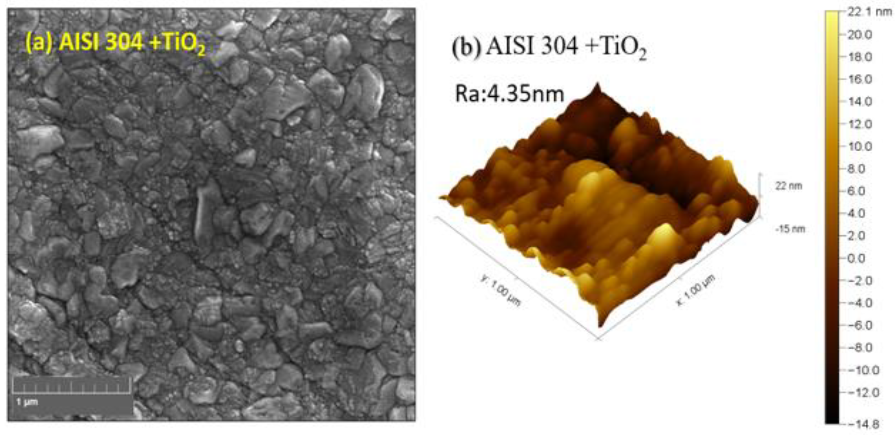
Figure 1a shows the SEM-FEG images of the TiO
2 thin film deposited on AISI 304. As the magnification increases,
Figure 1b shows the TiO
2 AFM image; it can be seen that the film is smooth, with a roughness of 4.35 nm, and densely covers the substrate. Also, it is possible to observe that the film is composed of tiny grains with irregular shapes and different sizes around tenths of nanometers, leading to a smooth surface.
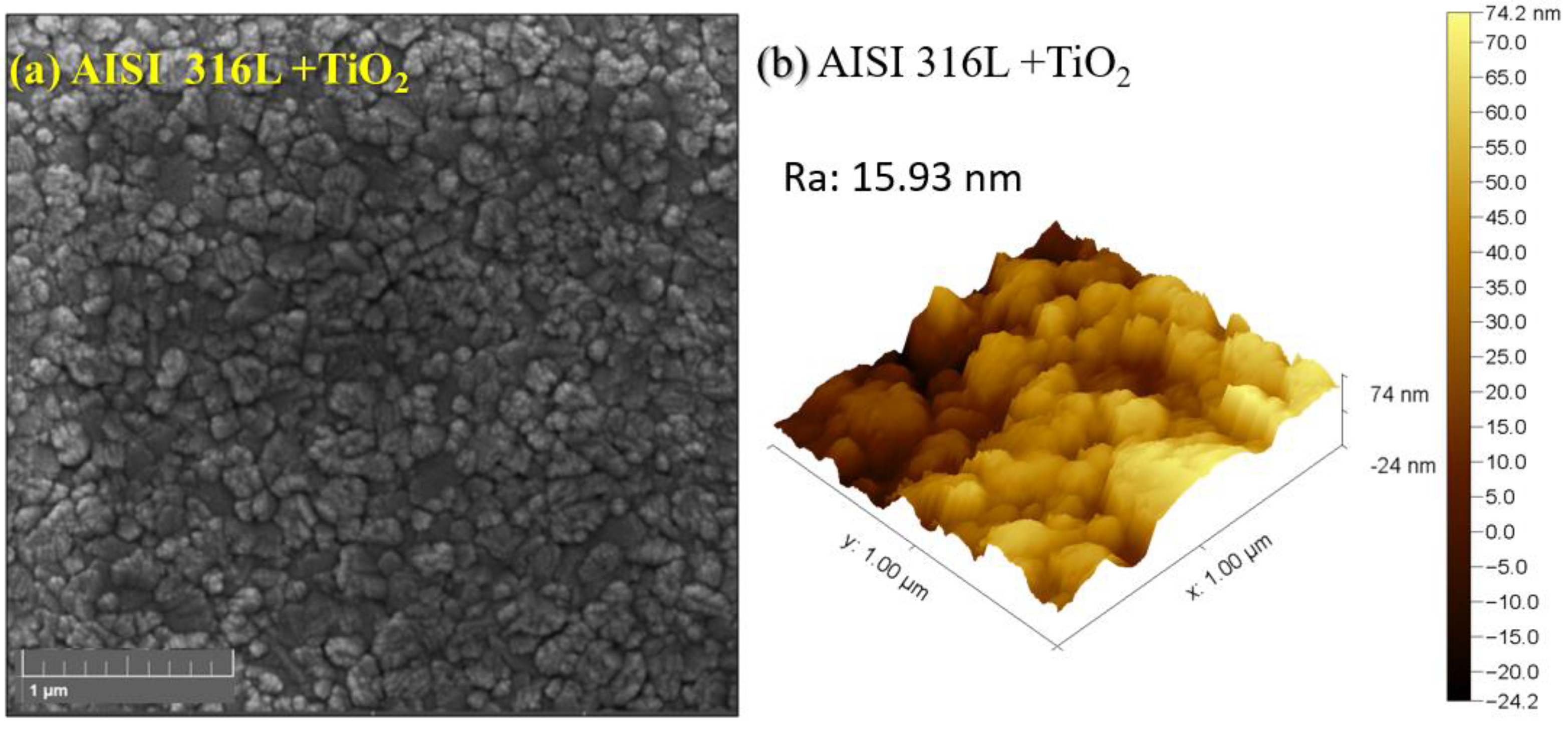
Figure 2a shows the SEM-FEG images of the TiO
2 thin film deposited on AISI 316L. As the magnification increases,
Figure 2b shows the TiO
2 AFM image; it can be seen that the film is smooth, with a roughness of 15.93 nm, and densely covers the substrate. Also, it is possible to observe that the film is composed of tiny grains with irregular shapes and different sizes around tenths of nanometers, leading to a smooth surface.
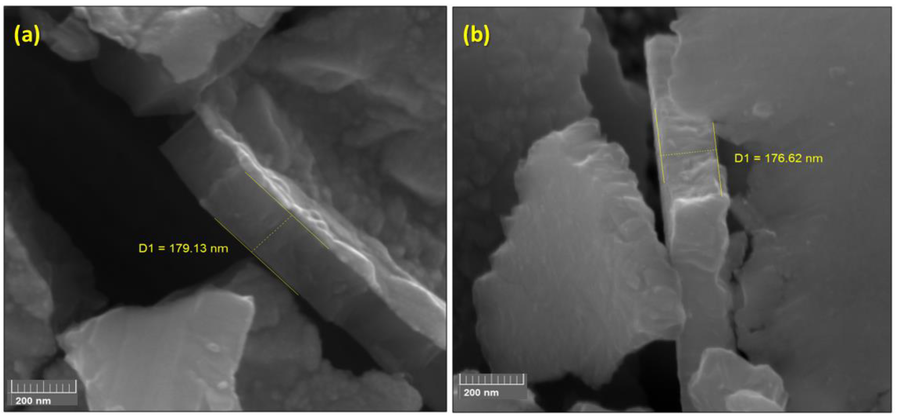
Figure 3 shows two images obtained from SEM-FEG microscopy after a deliberate fracture from AISI substrates.
Figure 3a shows the TiO
2 film thickness removed from AISI 304 (a) 179.1 nm, and (b) from TiO
2 film removed from AISI 316L 176.6 nm. This thickness corresponds to 3 thousand cycles of deposition process at 300 °C as described in the methodology. Leem J. and collaborators previously studied the correlation of cycles and thickness of the TiO
2 film. They analyzed the correlation of TiO
2 thickness using a typical sequence of TiCl
4 pulse-purge-H
2O pulse-purge around 300°C, and they reported film thickness reduction when they inserted HCl in a typical sequence of TiCl
4 pulse-purge-H
2O pulse-purge. They achieved a thickness of around 135 nm at 300 °C, compared with our results, using only a typical sequence of TiCl
4 pulse-purge-H
2O pulse-purge around 300°C, we obtained 24% higher for TiO
2 on AISI 304 and 23% higher on AISI 316L is 176.6 nm [
30].
3.2. Raman Spectroscopy
The TiO
2 film signature was evaluated by Raman spectroscopy.
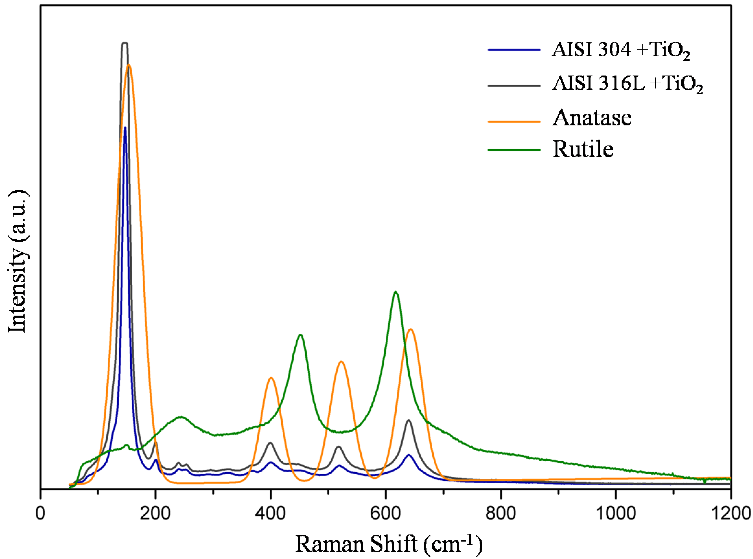
Figure 4 shows the Raman shift plot of TiO
2 film deposited on AISI 304 and AISI 316L substrates compared to anatase and rutile spectra. The Raman spectra of TiO
2 film on AISI 304 show the representative bands identified near 148 cm
-1; 200 cm
-1,240 cm
-1, and 252 cm
-1; 399 cm
-1; 451 cm
-1; 519 cm
-1, and 640 cm
-1. The Raman shift of TiO
2 film on AISI 316L shows the main bands centered on 146 cm
-1; 200 cm
-1, 238 cm
-1 and 254 cm
-1; 400 cm
-1; 449 cm
-1; 518 cm
-1 and 639 cm
-1. Analyzing the Raman spectra, the bands from 50 cm
-1 to 180 cm
-1 correspond to the anatase phase centered at 152 cm
-1. The corresponding bands of anatase and rutile phases were also shown by Evans and Sheel (2007) [
8]. From 180 cm
-1 to 300 cm
-1, the correspondent band in rutile is centered at 244 cm
-1 but appears in a wide band. The Raman spectra in both films show three bands in this region, as also observed by Rossela et al. (2010) [
11]. From 300 cm
-1 to 440 cm
-1, the bands from TiO
2 films deposited on AISI 304 and AISI 316L correspond to the anatase phase at 400 cm
-1, as observed by Hardcastle (2011) [
31]. From 440 cm
-1 to 500 cm
-1, both spectra show small bands centered near 450 cm
-1, corresponding to the rutile phase, Rosselaet al. (2010) [
11]. From 500 cm
-1 to 580 cm
-1 appears, a band in both spectra corresponding to the main band of anatase at 522 cm
-1, Hardcastle (2011) [
31]. Also, the spectra of AISI 304 and AISI 316L show bands from 580 cm
-1 to 800 cm
-1 corresponding to anatase at 642 cm
-1 and do not correspond to the rutile band at 616 cm
-1, Hardcastle (2011) [
31].
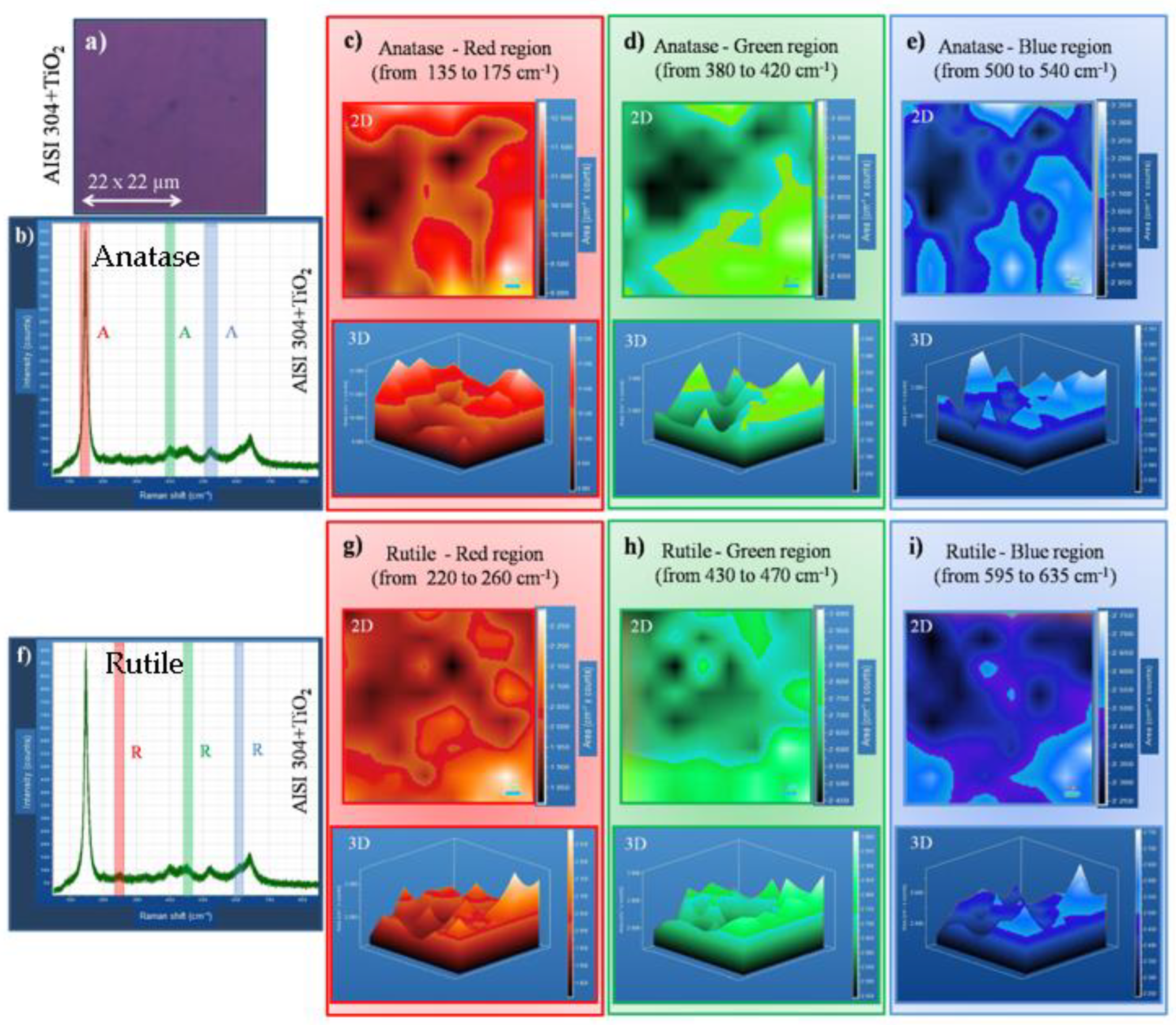
Raman mapping was performed to evaluate the distribution of anatase and rutile phases on the TiO
2 film deposited.
Figure 5 shows the data collected on AISI 304+TiO
2 sample. Anatase and rutile phases can be identified and are evenly distributed all over the film, on the surface (2D images), and in-depth (3D images).
Figure 5a Optical microscope image of the scanned area with 22 µm
2;
Figure 5b Raman shift plot with anatase bands was identified and can be visualized in red, blue, and green colors bar, for eyes direction.
Figure 5c,d shows 2D, and
Figure 5e–g shows 3D Raman mapping of anatase. The bands are localized in the region of Raman shift plot (c) 135 to 175 cm
-1 using (red bar); (d) 380 to 420 cm
-1 using (green bar), and (e) 500 to 540 cm
-1 using (blue bar).
Figure 5f shows the Raman shift plot with rutile bands identified; 2D and 3D Raman mapping from (g) 220 to 260 cm
-1 using (red-bar); (h) 430 to 470 cm
-1 using (green-bar) and (i) 595 to 635 cm
-1 using (blue)-bar.
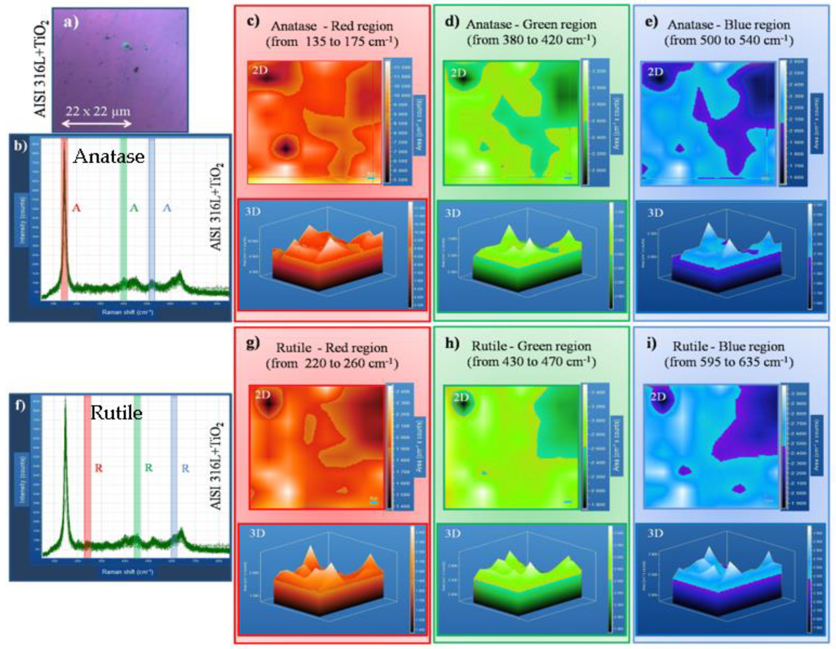
Figure 6c,d shows 2D, and
Figure 6e–g shows 3D Raman mapping of rutile deposited on the AISI 316L+TiO
2. Some details are explained hereafter:
Figure 6a shows the optical microscope image of the scanned area with 22 µm
2.
Figure 6b Raman shift plot with rutile bands was identified and can be visualized in red, blue, and green colors, and used color bars over the bands’ position for eyes direction.
Figure 6c,d shows 2D, and
Figure 6e–g shows 3D Raman mapping of the rutile phase on TiO
2 film. The rutile bands were centered in specific positions as can be seen in the red bar band, which was correlated with Figure (c) 135 to 175 cm
-1 (red); the green bar band that was correlated with
Figure 6d 380 to 420 cm
-1, and the blue bar band was correlated to
Figure 6e 500 to 540 cm
-1.
Figure 6f shows the 3D Raman shift plot with rutile bands identified; from Raman mapping (g) 220 to 260 cm
-1 (red), (h) 430 to 470 cm
-1 (green), and (i) 595 to 635 cm
-1 (blue). Also, all bands are well distributed in the analyzed area.
3.3. X-ray Diffraction
The results of the crystalline phase of TiO
2 films were evaluated by X-ray diffraction (XRD).
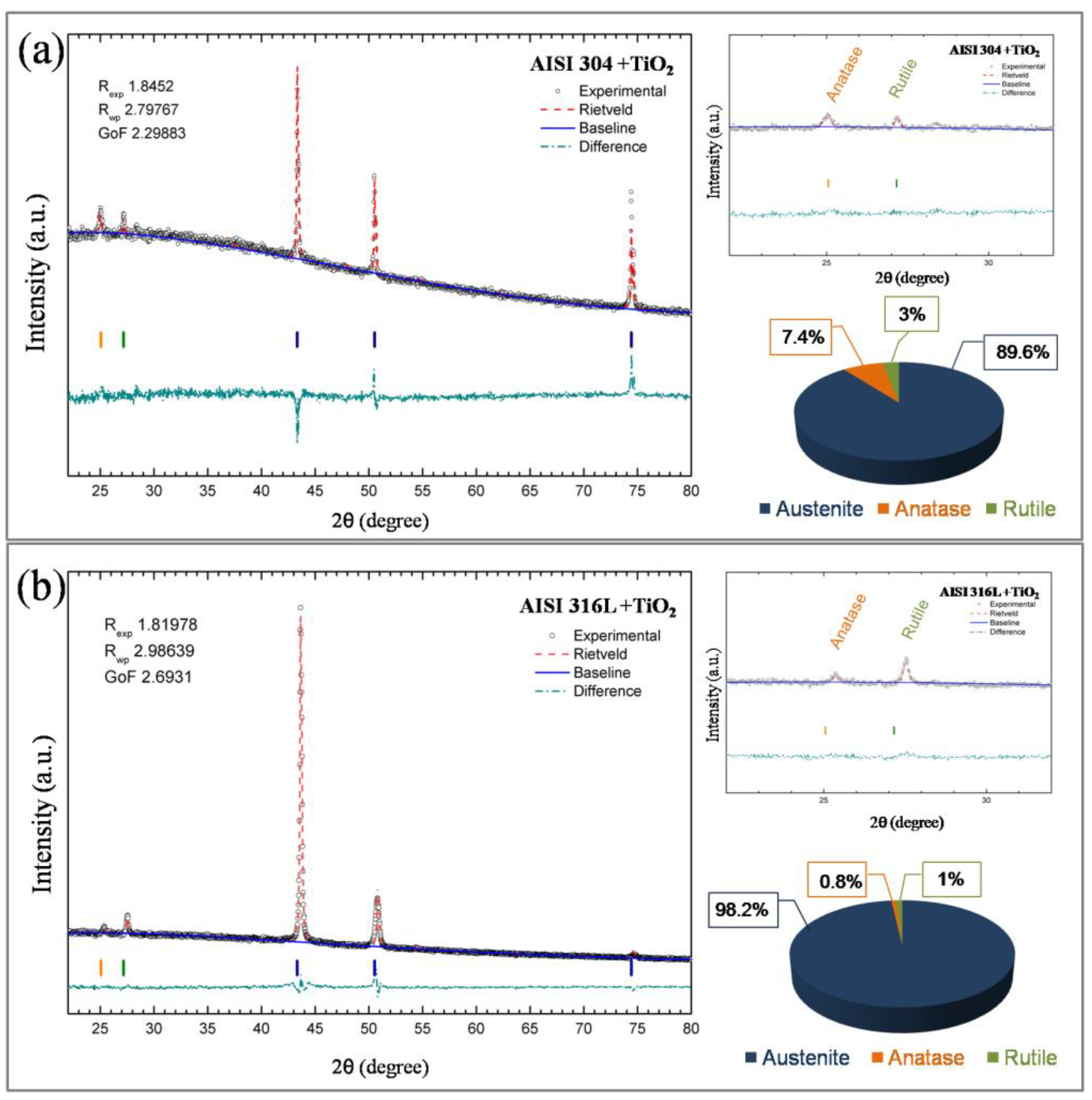
Figure 7 shows the XRD patterns of TiO
2 after treatments of the data with the Rietveld refinement method [
24]. According to the XRD results, it can be seen, in agreement with previous characterization by Raman spectroscopy, that the TiO
2 films are formed by the anatase and rutile phases. The XRD results of AISI 304 (
Figure 7a show that the anatase phase corresponds to 3% of the film, the rutile phase corresponds to 7.4%, and 89.6% is the austenite identified from AISI 304 substrate. In AISI 316L
Figure 7b, the anatase phase corresponds to 0.8% of the film, while the rutile phase corresponds to 1%, and 98.2% is austenite identified from the AISI 316L substrate.
The XRD and Raman results have not identified the brookite phase in the TiO2 film; those results show that the structure of the TiO2 films deposited onto AISI 304 and AISI 316L indicates that the crystalline phase of the film is composed of anatase and rutile phases.
3.4. Scratch Test—Adherence Film Evaluation
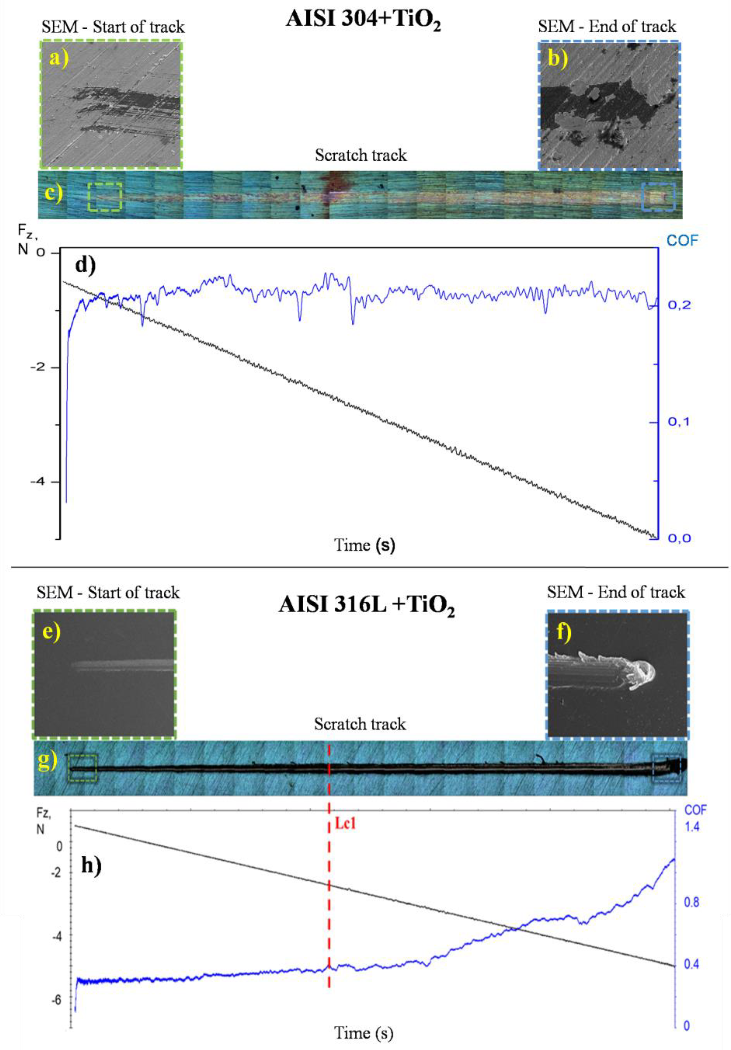
Figure 8a,b contains photomicrographs obtained via SEM of the start and end of the tracks formed after the scratch test on the AISI 304+TiO
2 sample. The end of the track, in
Figure 8b, indicates an adhesive failure with gross spallation according to ASTM C1624-05 [
29] in part of the film. However, a more detailed analysis of the SEM image makes it possible to identify the existence of TiO
2 particles covering the substrate in the delamination region, showing that the substrate is not exposed at the end of the scratching test.
The friction coefficient of TiO
2 film deposited on AISI 304 can be observed in
Figure 8d; the value is related to friction between a diamond tip and the TiO2 film under a progressive load till 5N. The friction behavior plot curve indicates that the film has well adhered to the substrate once the friction coefficient does not show a considerable variation on the length of the track and presents an average of around 0.2±0.05; the same value was found in previous work in our group around 0.19, ±0.05 as can be seen in Radi et al. (2018) [
32].
In
Figure 8e,f, SEM images of the start and end of the track, respectively, are shown. The end of the track indicates a cohesive failure by prow deformation in the TiO
2 film, according to Radi et al. 2018 [
32]; the track image was compared with the friction coefficient plot and normal force as a function of time obtained from the interaction of the diamond tip with the TiO
2 film on AISI 316L substrate during the scratch test. The friction coefficient, in
Figure 8h, started near 0.30 and ended near 1.10. The adherence value of the coating was derived from the Fz value, where the film failure occurred without substrate exposition (Lc1), which was found to be 2.4 N.
The TiO
2 film on AISI304 has a higher amount of anatase and rutile phases than the film on AISI 316L substrates, as indicated by XRD results. Also, Zalnezhad et al. [
14] described previously that the crystal structure of anatase (tetragonal) and the crystal structure of rutile is very similar, except that the octahedra share four edges in rutile instead of four corners in anatase, favoring the formation of chains, making the rutile structure more densely packed than anatase.
4. Conclusions
This study shows that TiO2 films deposited by atomic layer using a cycle of a typical sequence of TiCl4 pulse-purge-H2O pulse-purge at 300°C and three thousand cycles produce a heterostructure composed of anatase and rutile phases. A more crystallinity percentage was obtained on AISI 304, which presented 7.4% of anatase and 3% of rutile. On the other hand, the AISI 316L presented just 0.8 anatase and 1% of rutile. The Raman spectra confirmed the heterostructure in both TiO2 samples and showed that anatase and rutile are evenly distributed in the film. The adherence was better for TiO2 deposited on AISI 304, which kept the same friction coefficient average of around 0.2 and no evidence of cracks. On the other hand, the TiO2 deposited on AISI 316L presented a critical load (Lc1) without substrate exposition around 2.2N. The TiO2 film presented in this work had a thickness 24% higher than the literature for TiO2 film on AISI 304 and 23% for TiO2 film on AISI 316L. Finally, the results show an improvement of crystallinity around 82% for TiO2 deposited on AISI 304.
Acknowledgments
The authors are grateful to INPE for using the scanning electron microscope and Raman system, ITA for using XRD equipment, and UNICAMP for the atomic force microscope. We also thank IP&D – UNIVAP for the ALD facilities.The following Brazilian research agencies have supported this work: Grant #11/50773-0 São Paulo Research Foundation (FAPESP), also financial in part by the CAPES - Coordenação de Aperfeiçoamento de Pessoal de Nível Superior grant #001, and, also by CNPq - Conselho Nacional de Desenvolvimento Científico e Tecnológico, grant # 317253/2021-2.
Conflicts of Interest
The authors declare no conflict of interest.
References
- J. Zheng, S. Bao, Y. Guo, and P. Jin, “TiO2 films prepared by DC reactive magnetron sputtering at room temperature: phase control and photocatalytic properties. Surf. Coat. Technol. 2014, 240, 293–300. [Google Scholar] [CrossRef]
- E. M. Kiarii, K. K. Govender, P. G. Ndung, and P. P. Govender, “The generation of charge carriers in semiconductors - A theoreical study. Chem. Phys. Lett. 2017, 678, 167–176. [Google Scholar]
- M. Grao, M. Ratova, C. C. Amorim, R. B. P. Marcelino, and P. Kelly, “Crystalline TiO2 supported on stainless steel mesh deposited in a one step process via pulsed DC magnetron sputtering for wastewater treatment applications. J. Mater. Res. Technol. 2020, 9, 5761–5773. [Google Scholar] [CrossRef]
- I. V. L. Ferreira and L. A. Daniel, “TiO2 Heterogeneous photocatalysis in secondary wastewater treatment. Eng. Sanit. Ambient. 2004, 9, 335–342. [Google Scholar]
- Q. Seul-yi and S. Park Review of TiO2 photocatalyst for water treatment applications. J. Ind. Eng. Chemestry, 2013, 19, 1761–1769. [Google Scholar] [CrossRef]
- M. Reid et al. How Does a Photocatalytic Antimicrobial Coating Affect Environmental Bioburden in Hospitals. Infect. Control Hosp. Epidemiol. 2018, 39, 1–7. [Google Scholar]
- H. M. Wadullah, S. A. 7. H. M. Wadullah, S. A. Ajeel, and M. K. Abbass Synthesis and Characterization of Nanocoatings Thin films by Atomic Layer Deposition for Medical Applications. IOP Conf. Ser. Mater. Sci. Eng. 2019, 518. [Google Scholar] [CrossRef]
- P. Evans and D. W. Sheel Photoactive and antibacterial TiO2 thin films on stainless steel. Surf. Coatings Technol. 2007, 201, 9319–9324. [Google Scholar] [CrossRef]
- R. Thiruvenkatachari, S. Vigneswaran, and I. S. Moon A review on UV/TiO2 photocatalytic oxidation process. Korean J. Chem. Eng. 2008, 25, 64–72. [Google Scholar] [CrossRef]
- J. Feltrin Estabilização a elevadas temperaturas da fase anatase com partículas submicrométricas de SiO2”,Dissertação de mestrado, Universidade Federal de Santa Catarina, 2012.
- F. Rossella et al. TiO2 thin films for spintronics application: a Raman study. J. Raman Spectrosc. 2010, 41, 558–565. [Google Scholar] [CrossRef]
- C. X. Shan, X. Hou, and K. Choy Corrosion resistance of TiO2 films grown on stainless steel by atomic layer deposition. Surf. Coat. Technol. 2008, 202, 2399–2402. [Google Scholar] [CrossRef]
- T. Yeh, Y. Huang, M. Wang, and C. Tsai Hydrothermal treatments of TiO2 on Type 304 stainless steels for corrosion mitigation in high temperature pure water. Nucl. Eng. Des. 2013, 254, 228–236. [Google Scholar] [CrossRef]
- E. Zalnezhad, A. M. S. Hamuda, G. Faraji, and S. Shamshirband TiO2 nanotube coating on stainless steel 304 for biomedical applications. Ceram. Int. 2014, 41, 2785–2793. [Google Scholar]
- S. Ali et al., Microstructure and Mechanical Properties of Modified 316L Stainless Steel Alloy for Biomedical Applications Using Powder Metallurgy. Materials 2022, 15, 2822. [Google Scholar] [CrossRef] [PubMed]
- L. Cardenas et al. Reduced graphene oxide growth on 316L stainless steel for medical applications. Nanoscale 2014, 6, 8664–8670. [Google Scholar] [CrossRef] [PubMed]
- N. Simionescu, L. Benea, and V. M. Dumitrascu The Synergistic Effect of Proteins and Reactive Oxygen Species on Electrochemical Behaviour of 316L Stainless Steel for Biomedical Applications. IOP Conf. Ser. Mater. Sci. Eng. 2018, 374, 1–7. [Google Scholar]
- H. Zhang and J. F. Banfield Structural characteristics and mechanical and thermodynamic properties of nanocrystalline TiO2. Chem. Rev. 2014, 114, 9613–9644. [Google Scholar] [CrossRef] [PubMed]
- M. F. Pillis, M. C. L. de Oliveira, O. V. Correa, and R. A. Antunes Efeito de filmes de TiO2 obtidos pelo processo de deposição química de organometálicos em fase vapor (MOCVD) sobre a resistência à corrosão do aço inoxidável AISI 304. Intercorr 2012, 2012, 1–9. [Google Scholar]
- I. S. Brandt et al. Influence of substrate on the structure of predominantly anatase TiO2 films grown by reactive sputtering. R. Soc. Chemestry Adv. 2018, 8, 7062–7071. [Google Scholar]
- A. A. Vieira et al. Tribocorrosion Susceptibility and Osseointegration Studies of Silicon – Carbon – Titanium Oxide Coatings Produced on SS316L by Laser Cladding. J. Bio- Tribo-Corrosion 2020, 7, 10. [Google Scholar]
- Z. Xing et al. Recent advances in floating TiO2-based photocatalysts for environmental application. Appl. Catal. B, Environ. 2018, 225, 452–467. [Google Scholar] [CrossRef]
- J. Aarik, J. Karlis, H.MaÈndar, T. Uustare, and V. Sammelselg Influence of structure development on atomic layer deposition of TiO2 thin films. Appl. Surf. Sci. 2001, 181, 339–348. [Google Scholar] [CrossRef]
- H. M. Rietveld The Rietveld method. Phys. Scr. 2014, 89. [Google Scholar]
- T. Degen, M. T. Degen, M. Sadki, E. Bron, U. König, and G. Nénert The HighScore suite. Powder Diffr., 29, no. S2, S13–S18, 2014.
- M. Horn, C. F. Schwebdtfeger, and E. P. Meagher Refinement of the structure of anatase at several temperatures. Cryst. Mater. 1972, 136, 273–281. [Google Scholar]
- V. W. H. Baur Über die Verfeinerung der Kristallstrukturbestimmung einiger Vertreter des Rutiltyps: TiO2, SnO2, GeO2 und MgF2. Acta Crystallogr. 1956, 9, 515–520. [Google Scholar] [CrossRef]
- M. E. Straumanis and D. C. Kim Lattice Constants, Thermal Expansion Coefficients, Densities and Perfection of Structure of Pure Iron and of Iron Loaded with Hydrogen. Int. J. Mater. Res. 1969, 60, 272–277. [Google Scholar] [CrossRef]
- I.C1624-05 (2015) Standard Test Method for Adhesion Strength and Mechanical Failure Modes of ceramic coatings by quantitative single point scratch testing. ASTM international, C1624-05, no. Reapproved 2012, 1–29.
- J. Leem et al. Role of hcl in atomic layer deposition of TiO2 thin films from titanium tetrachloride and water. Bull. Korean Chem. Soc. 2014, 35, 1195–1201. [Google Scholar] [CrossRef]
- F. D. Hardcastle Raman Spectroscopy of Titania (TiO2) Nanotubular Water- Splitting Catalysts. J. Ark. Acad. Sci. 2011, 65, 43–48. [Google Scholar]
- P. A. Radi, et al. Tribocorrosion behavior of TiO2/Al2O3 nanolaminate, Al2O3, and TiO2 thin films produced by atomic layer deposition. Surf. Coat. Technol. 2018, 349, 1077–1082. [Google Scholar] [CrossRef]
|
Disclaimer/Publisher’s Note: The statements, opinions and data contained in all publications are solely those of the individual author(s) and contributor(s) and not of MDPI and/or the editor(s). MDPI and/or the editor(s) disclaim responsibility for any injury to people or property resulting from any ideas, methods, instructions or products referred to in the content. |
© 2023 by the authors. Licensee MDPI, Basel, Switzerland. This article is an open access article distributed under the terms and conditions of the Creative Commons Attribution (CC BY) license (http://creativecommons.org/licenses/by/4.0/).
