Introduction
Power electronic converters, such as dc-dc converters, are typical piecewise smooth circuit systems due to the turn-on and turn-off effects of power switches, and their performance is closely related to operation conditions. It is generally believed that, when the load or power source fluctuates, or the parameters of passive components are not properly configured, one may be able to observe nonlinear dynamic phenomena such as bifurcations and chaos in power electronic converters, which are undesired in practical applications [
1]. For instance, the active duty ratio of a PCMC dc-dc boost converter is generally limited to less than
in continuous conduction mode (CCM), because when the ratio exceeds this range, the converter will be in period-2 sub-harmonic oscillation state, so the voltage boost capability is limited in applications [
2].
In order to better predict the nonlinear phenomena of power electronic converters and provide design-oriented guidance in practice, lumped parameter models and integer-oder piecewise linear differential equations are widely adopted to describe the the electrical relationship of the state variables of power electronics converters [
3]. To analyze the nonlinear behaviours of the converters, one can solve the initial value problem (IVP) of integer-oder ordinary differential equations (ODEs) by both numerical and analytical calculation methods, and use the stroboscopic map technique to sew up the solutions of piecewise linear differential equations [
4]. Based on these methods, a large number of researches have been conducted to explore nonlinear dynamic phenomena in power electronic converters, such as those surveyed in literature [
5,
6,
7].
By reviewing the key publications in the related field, one can find that, the parameters of traditional lumped parameter models usually appear in the form of parameter variables (or parameter vector), while in the solving process of IVP, these parameter variables are usually substituted with constant nominal values or the measured constant values under a fixed condition. However, not only the load and power supply may change, but also some other electronic components may experience parameter drift in practice [
8,
9,
10,
11]. For instance, non-solid electrolytic aluminum capacitors are widely adopted in power electronic converters, but their capacitance and equivalent series resistance (ESR) can be easily affected by operating frequency, working temperature, and so on. In order to reflect the impacts of parameter variations on the nonlinear characteristic of converters, one can draw bifurcation diagrams by changing the parameters of traditional lumped parameter models, but the model itself cannot reflect the parameter drift of the components. That is to say, traditional models cannot reflect the correlation between the microscopic characteristics of electronic components and the macroscopic electrical characteristics of converter systems. The results obtained by using traditional integer-order models may be biased in practice. Therefore, it is worthwhile to develop more precise and reliable methods to address the aforementioned concerns.
In recent decades, exploring the characteristics of electronic components arouses ever-increasing attention in circuit theory and application fields [
12], and a rich source of evidence suggests that the characteristics of electronic components can be more effectively captured by using the concepts of fractional calculus compared to classical calculus-based models [
13,
14,
15], and factional-order impedance (or constant phase elements, CPEs) based models have been widely adopted to describe the characteristics of electronic components, such as inductors [
16], ultracapacitors (UCs) [
17,
18], lithium batteries [
19], power MOSFETs [
20], and non-solid electrolytic capacitors [
21]. Therefore, using this model to bridge the gap between the microscopic characteristics of electronic components and the macroscopic characteristics of circuit systems has become a hot issue in recent years.
In this paper, taking a PCMC dc-dc boost converter as an example, we study the nonlinear characteristics of the converter with a fractional-order output filtering capacitor, and we carried out the following works:
A piecewise smooth non-commensurate fractional-order model is developed for a PCMC dc-dc boost converter, which contains a fractional-order output filtering capacitor and a detailed control loop design based on a type UC3842 PCMC power management chip.
A large-signal stability analysis is performed for the converter, in which the fractional Adams-Bashforth-Moulton typed method (F-ABM) and stroboscopic map technique are applied for tiem-domain calculation, while bifurcation diagrams are obtained for dynamic states justification.
Both circuit-level simulations and experiments are provided to verify the correctness of the theoretical analysis.
To present the above features in detail, the rest of this paper begins with the derivation of the piecewise smooth model of the converter in section II. After that, a detailed nonlinear dynamic characteristic analysis of the converter is provided in section III. Then, in section IV, both the circuit-level simulation platform and experiment prototype are established, and the results are provided for validation and comparison. Finally, conclusion is outlined in Section V.
2. Piecewise Smooth Fractional-Order Model of PCMC DC-DC Boost Converters
2.1. Circuit configuration
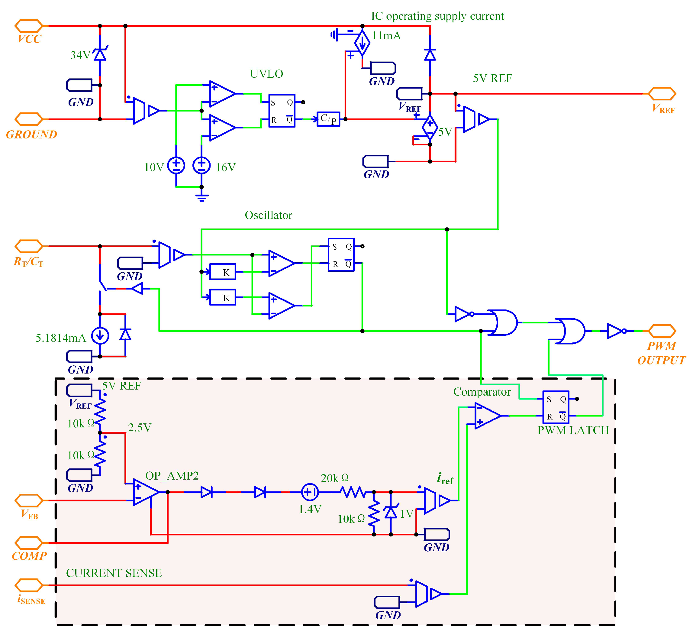
It is a fast and cost effective option to use power management chip to control dc-dc converters in application. In this work, we use a type-UC3842 power management chip, which is a fixed frequency current-mode controllers [
21], its internal structure is as depicted in
Figure 1.
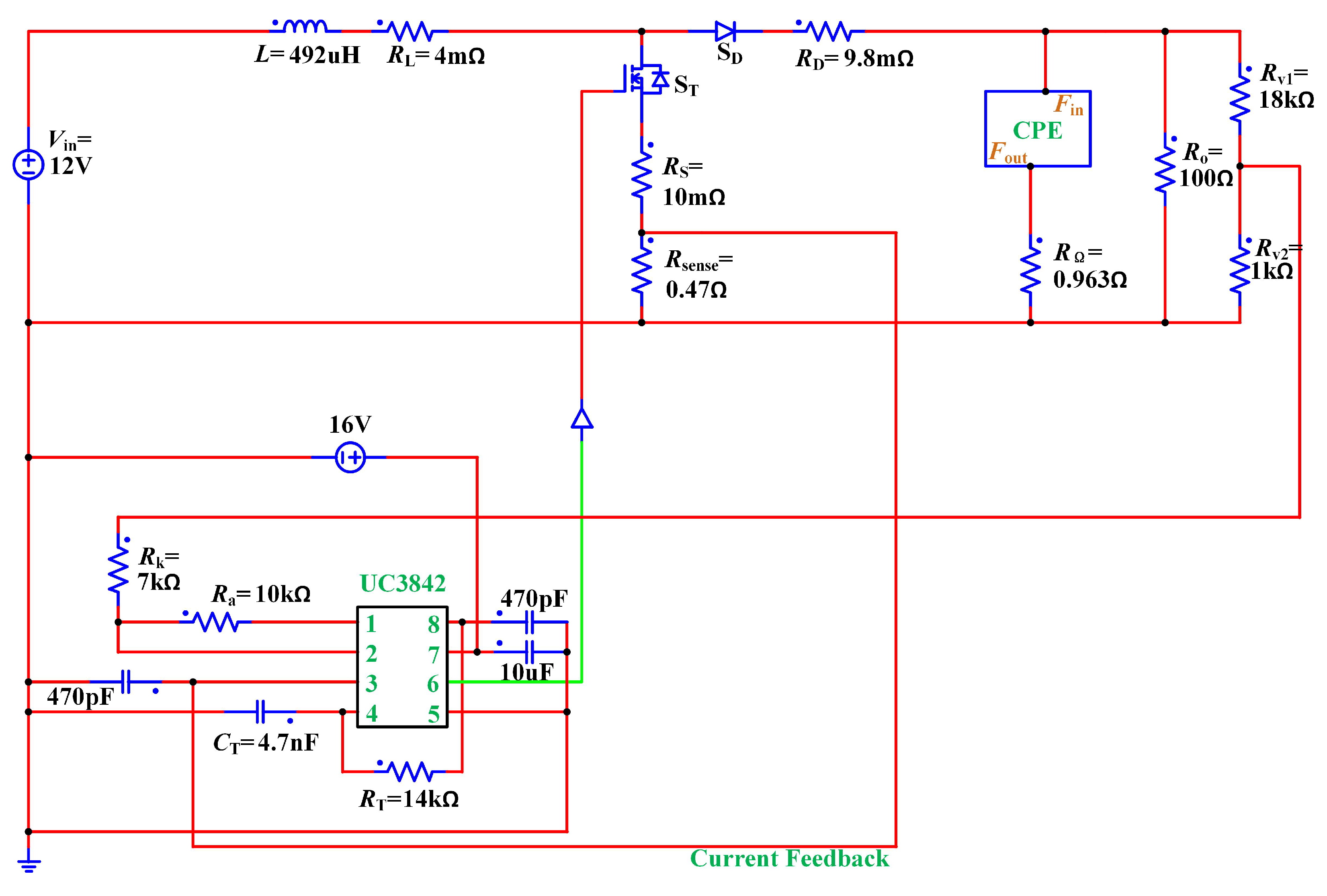
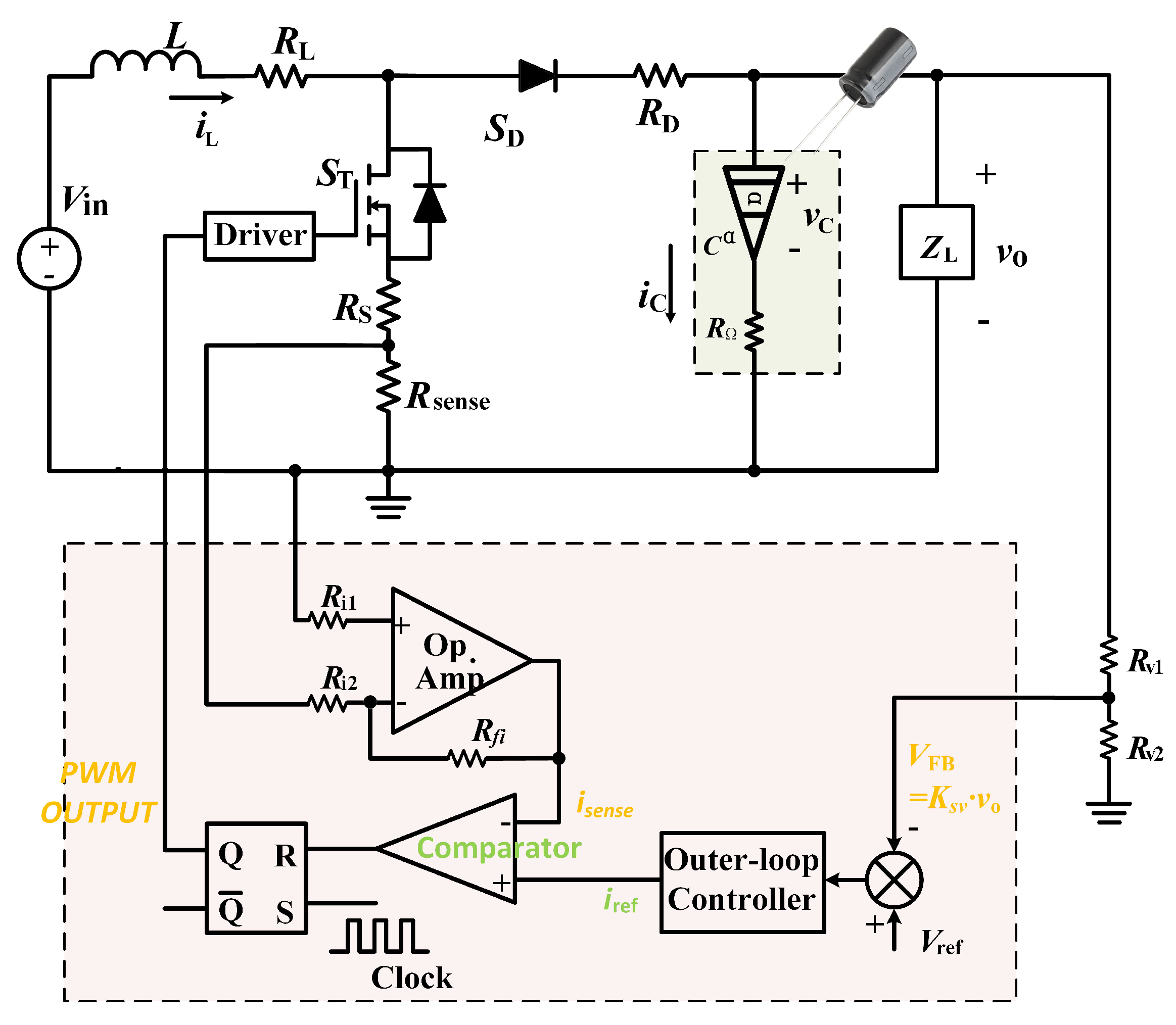
By adopting this chip to a dc-dc boost converter, one can achieve a PCMC design, the schematic diagram of which is depicted in
Figure 2.
Note that the output filtering capacitor in
Figure 2 is a non-solid electrolytic capacitor. According to a previous work [
23], the capacitance and the equivalent series resistance of the capacitor have frequency-related fractional-order characteristics in a wide frequency band. Therefore, we use a fractional-order equivalent impedance model to represent it, where an ideal fractional-order capacitor
(or constant phase element, CPE) is in series with an estimated equivalent series resistance
. The symbol
C is the nominal capacitance of the capacitor and the symbol
is the estimated fractional order of the capacitor.
In addition, note that in both
Figure 1 and
Figure 2, the two boxes with red background correspond to the same function module. Specifically, there are the same output voltage current sensing unit, inductor current sensing unit, the inner curent loop controller, and the outer voltage loop controller. The inner current loop usually includes an inductor current sensing resistor
, and a proportional sampling unit is used to sample the inductor current
. The
pin of the UC3842 chip is connected to a voltage divider composed by two resistors
and
, which is used to sample the output voltage
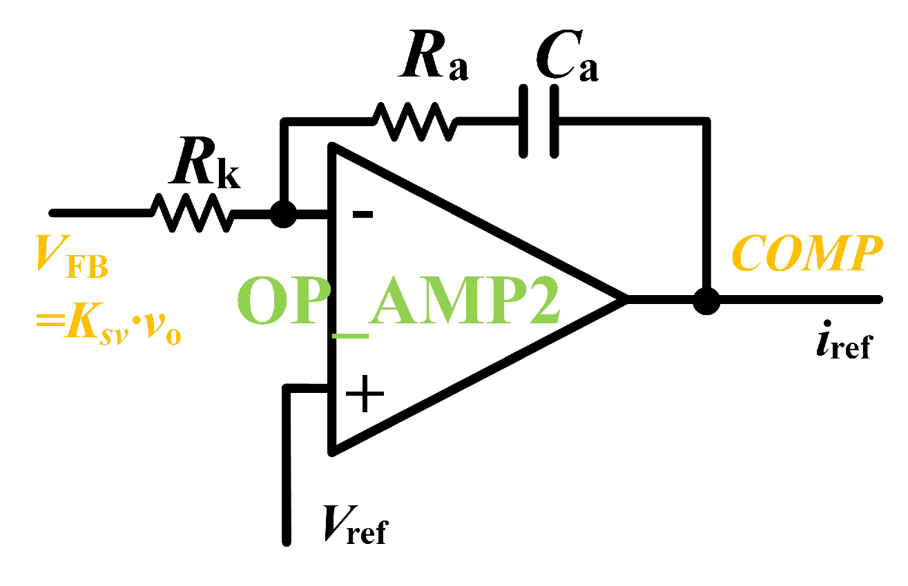
. The outer-loop controller can be achieved by configuring the circuit between the
pin and the
pin of the chip. For example, if one wants to used a typical PI controller in the outer loop, then one can configure the above two pins of the operational amplifier
as follows.
According to the above
Figure 3, one can deduce the the output of the outer voltage loop, or the reference signal
of the inner current loop, as follows.
If one uses a typical proportional controller for the outer voltage loop, then the the output of the outer voltage loop, or the reference signal
of the inner current loop, will be as follows.
in which the symbol
is the sampling ratio for the output voltage
, the value of which is determined by
. In addition, one can obtain the values of the proportional and integral coefficients
and
are
and
, respectively.
Meanwhile, the sampling current
is:
in which the symbol
is the sampling ratio for the inductor current
, the value of which is determined by
,
,
, and
.
According to the schematic and the working principle, the output of the outer voltage loop is employed as the reference signal of the inner current loop. The comparison result of two signals and is sent to an R-S trigger, the output of which is fed to two driving circuits to control the turn-on and off state of two power MOSFETs and .
2.2. Fractional-order piecewiese smooth model
Because of the turn-on and turn-off operations of power MOSFETs and , the converter is a typical piecewise smooth dynamic system. If one uses a proportional controller for the outer loop, and takes the inductor current and the voltage of the CPE as state variables, the converter will have a state vector of , and the switching modes of the converter can be governed by:
Switching mode 1: When the power MOSFETs
is on and
is off, the state of the converter can be governed by:
Switching mode 2: When the power MOSFETs
is off,
is on, and the inductor current is not 0, the state of the converter can be governed by:
Switching mode 3: When the power MOSFETs
is off,
is on, and the inductor current is 0, the state of the converter can be governed by:
According to the internal structure of
Figure 1 and the schematic of
Figure 2, when the output of the outer voltage loop is less than
, the switching condition of switching modes 1 and 2 is:
in which the term
corresponds to the forward voltage of two series diodes, which are in series with the output of the voltage controller. In addition, the coefficient
comes from the voltage divider of two resistors
and
, which are in series with the two diodes. These details can be found in
Figure 1.
When the output of the outer voltage loop is not less than
, the reference signal
will be clamped at
, and the switching condition of switching modes 1 and 2 will be:
At the switching-mode transition time , the condition of is satisfied, thus one can obtain the duty cycle . In steady state, if the converter works in the current continuous mode (CCM), that is, the current does not drop to 0 at the end of switching mode 2, the converter switches between switching modes 1 and 2 periodically.
3. Time-Domain Analysis
To reveal the time-domain performances and nonlinear dynamic characteristics of the PCMC DC-DC boost converter, the state equations
4 to equations
6 should be calculated, which are all fractional-order ordinary differential equations (FO-ODEs). Basically, these FO-ODEs can be generalized by the following following initial value problem (IVP)
in which the term
is the non-commensurate order vector, the function
, and the operator
is the differential operator of order
q.
3.1. Preliminaries: Principles of Some Related Techniques
To solve the above IVP, this section introduces the principle of fractional Adams-Bashforth-Moulton typed method (F-ABM), and applies the stroboscopic map technique to cope with piecewise smooth situations.
3.1.1. F-ABM calculation method
In case of
, according to the definition of F-ABM method [
23], the IVP of the fractional-order system of Equation
9 can be determined by:
where the term
n is any integer and
is
The predictor
in Equation
9 is
in which the term
is
Note that, the term
h in equation
10 and equation
13 is a predetermined step size, the value of which is defined according to the switching period
of the converter. In this work, we will set the step size to
of the switching period
, which satisfies the Nyquist sampling theorem.
3.1.2. Stroboscopic map technique
As introduced in section 1.2, the state of the converter cycles between switching mode 1 and switching mode 2 in each switching period in CCM. Along with the on- and off operations of power MOSFETs
and
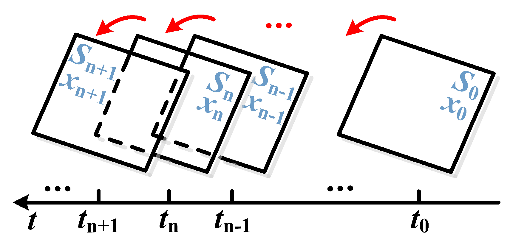
, there are a set of discontinuous points. Accordingly, a technique called stroboscopic map should be employed in calculations. This technique has been widely adopted in the dynamic analysis of piecewise-smooth systems and switching power converters. The principle of stroboscopic map technique is depicted in
Figure 4.
By this technique, the dynamic behavior of the converter at each switching mode will be collected in one switching cycle, that is, the solution of the previous switching mode at time will be employed as the initial value of the next switching mode, thus a cycle-by-cycle calculation can be carried out.
3.2. Bifurcation analysis
According to the discrete form of the obtained fractional-order piecewise smooth model, one can carry out the cycle-by-cycle numerical simulation for the converter in
Figure 1. In simulation, the parameters are as
Table 1.
Note that in the above table, the fractional order
and the ESR
of the output filtering capacitor are obtained by using a LCR meter and the parameter estimation method developed in [
21]. According to
Table 1, the sampling ratio
of inductor current equals to
, the sampling ratio
of the output voltage equals to
, and the proportional coefficient
of the outer voltage loop controller equals to
.
Then by using the F-ABM method to calculate equation
4 to equation
6, and by sewing up the solutions of these equations end to end by the stroboscopic map technique, one can obtain the bifurcation diagrams of state variables versus different parameters, such as
versus power supply
,
versus load resistance
, and
versus output voltage divider resistance
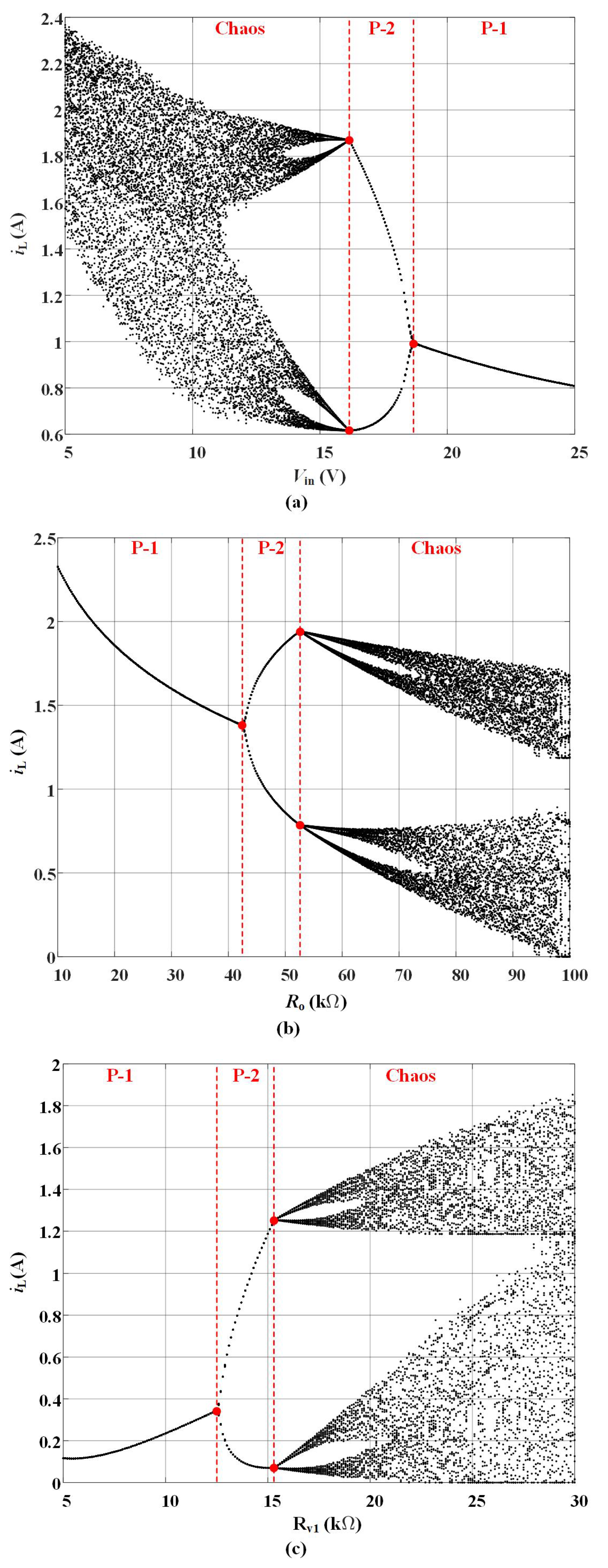
, as depicted in
Figure 5.
In
Figure 5, one can find that, the PCMC dc-dc boost converter enters chaotic state through period-doubling bifurcation in three cases. Specifically, when one set the load resistance
to be
, the compensation resistors of voltage loop controller
,
, the voltage divider resistor
,
, and other parameters to be as those listed in
Table 1, the converter keeps in chaotic state when the power supply is lower than
. Increasing the power supply above this value will lead to the converter enters period-2 (P-2) sub-harmonic oscillation state. After around
, the converter will be in period-1 (P-1) stable state. As to the load variation situation, when one set the power supply
to be
and other parameters as in the previous case, the converter will be in P-1 stable state when the load resistance
is less than
. After around
, the converter enters chaos. In addition in the output-voltage sampling ratio variation situation, when one set the power supply
to be
, the load resistance
to be
, and other parameters as in the previous case, the converter will be in P-1 stable state when the resistance
is less than
, and the converter will fall into chaos when the resistance
is greater than
.
4. Validation and Comparison
4.1. Circuit-level simulation
In order to validate the results of theoretical analysis, circuit-level simulation is conducted in PSIM software in this section, the schematic of the simulation paltform is as follows:
Figure 6.
Circuit-level simulation in PSIM software.
Figure 6.
Circuit-level simulation in PSIM software.
In the above schematic, the PCMC module UC3842 is actually
Figure 1, the CPE module, or an ideal order-
CPE, is constructed based on the rational approximation method, which has been used in a previous work [
25]. The details of the rational approximation circuit is as
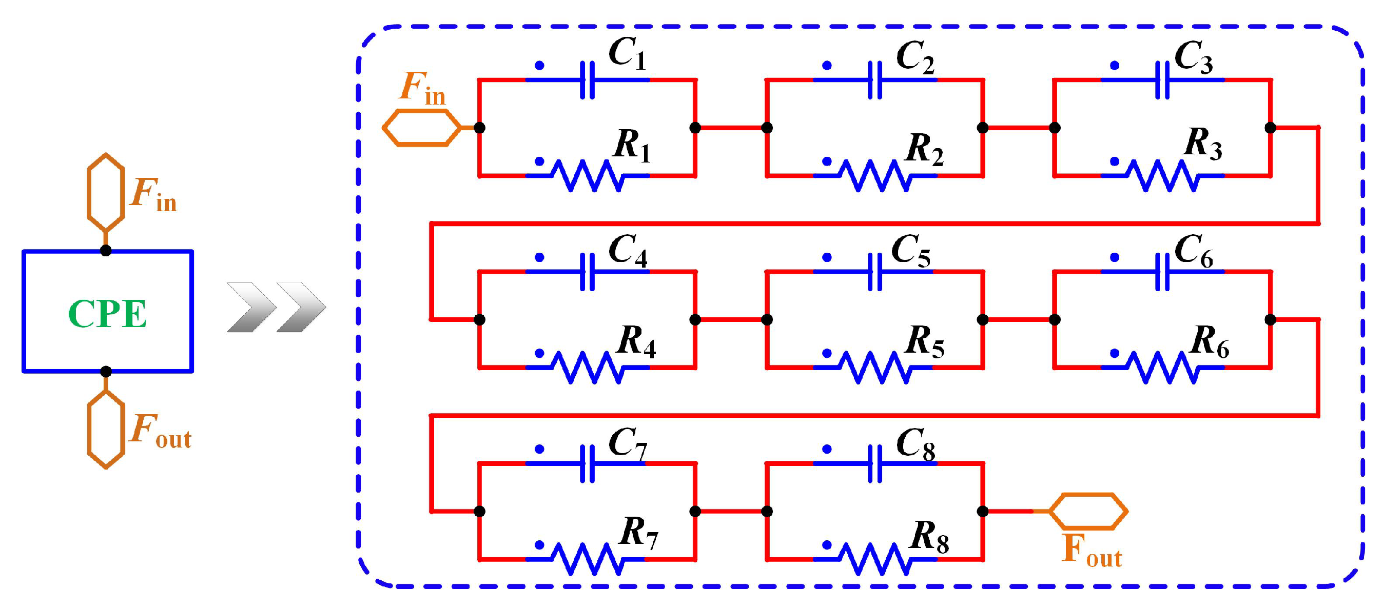
Figure 7, in which the rational approximation circuit of
CPE contains eight groups of R-C parallel unit. These groups are in series one by one, their vaules are obtained by a frequency-domain approximation method proposed in literature [
26,
27,
28] and the circuit network synthesis method adopted in previous work [
25,
29], in which we set the approximate phase error is within
. The detailed values of the CPE is listed in
Table 2.
By using the values of
and
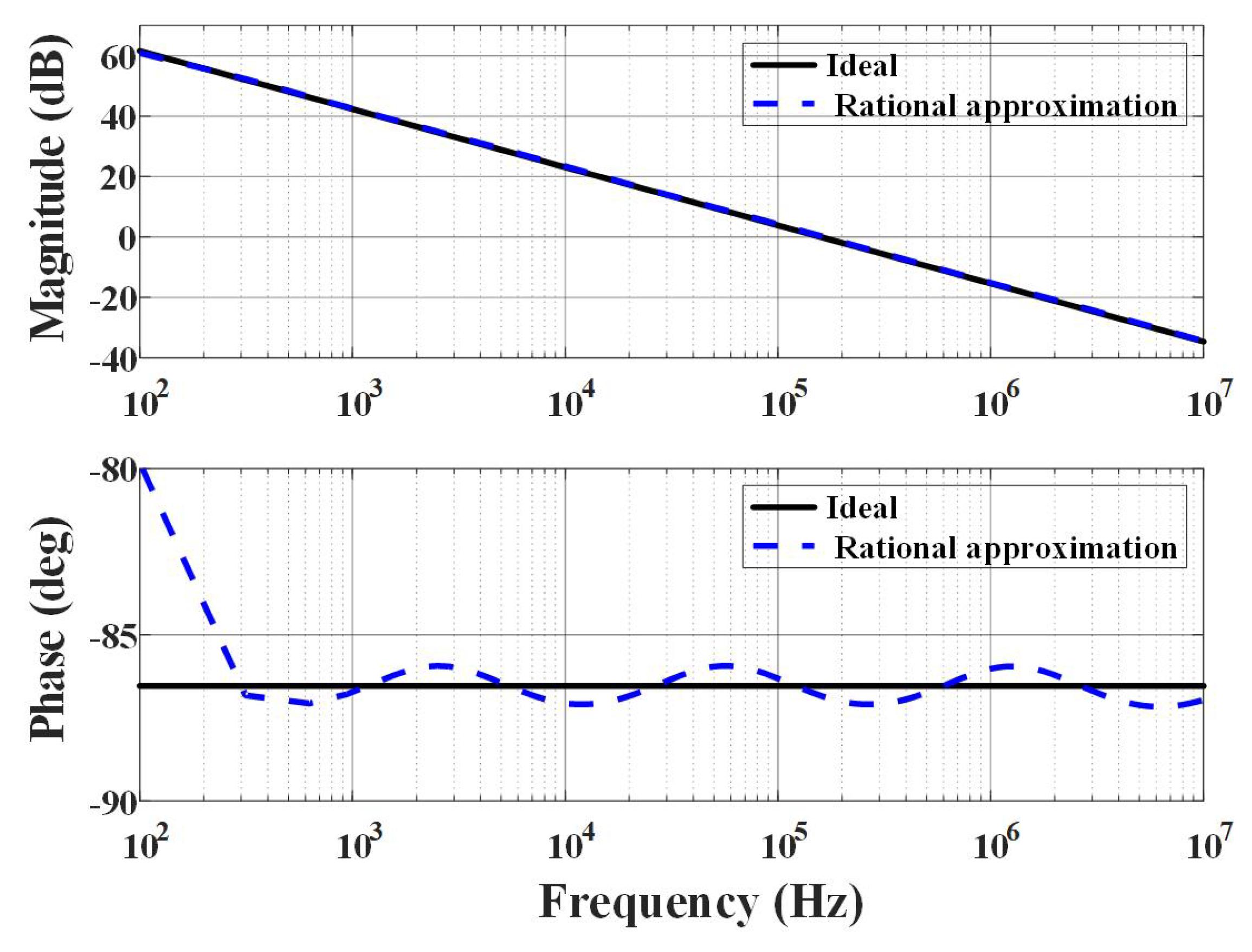
listed in the above table, one can plot the Bode diagrams of the constructed CPE, as dipicted in
Figure 8, in which the black solid lines represent the ideal order-
CPE and the blue dash curves belong to the devices obtained by rational approximation method and synthesis method.
Additionally, one can obtain the theoretical impedance
and the synthesis impedance
of the
capacitor as follows.
respectively. And one can find that the errors of the real part and the imaginary part of the two impedance are
and
, respectively. These error can be reduced by using a lower approximate phase error, but it will lead to an increase in the numbers of
units in the chain structure, as those discussed in literature [
25] and [
29]. It can be seen from
Figure 8 and Equation
14 that, both the frequency characteristic curves and two impedance values meet well with each other. It means that the constructed CPE can be used in simulation for validation.
Then one can use the constructed order-
CPE in PSIM software to obtain the time-domain results of the PCMC dc-dc boost converter. In the first place, we set the voltage dividing resistor
, the time-domain results of circuit-level simulation in PSIM software is as the following
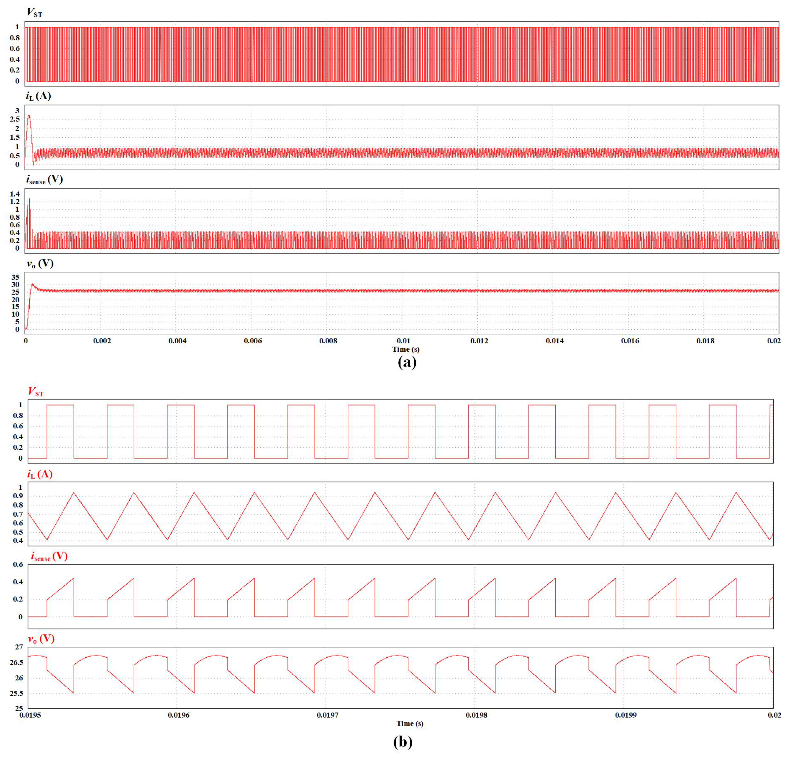
Figure 9.
In the figure above, from top to bottom, sub-figures correspond to the G-S voltage of power switch , the inductor current , the sampling value of the inductor current (which is actually the voltage of ), and the output voltage . One can find that, the PCMC dc-dc boost is in P-1 stable state under the configuration of parameters. The result is consistent with the results of bifurcation diagrams.
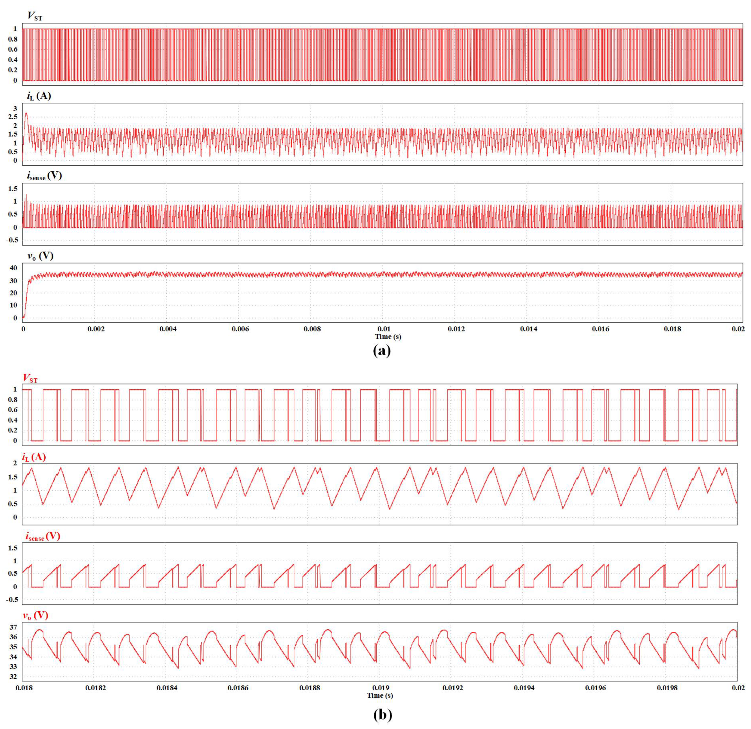
Then, we set the voltage dividing resistor
, the time-domain results of circuit-level simulation in PSIM software is as
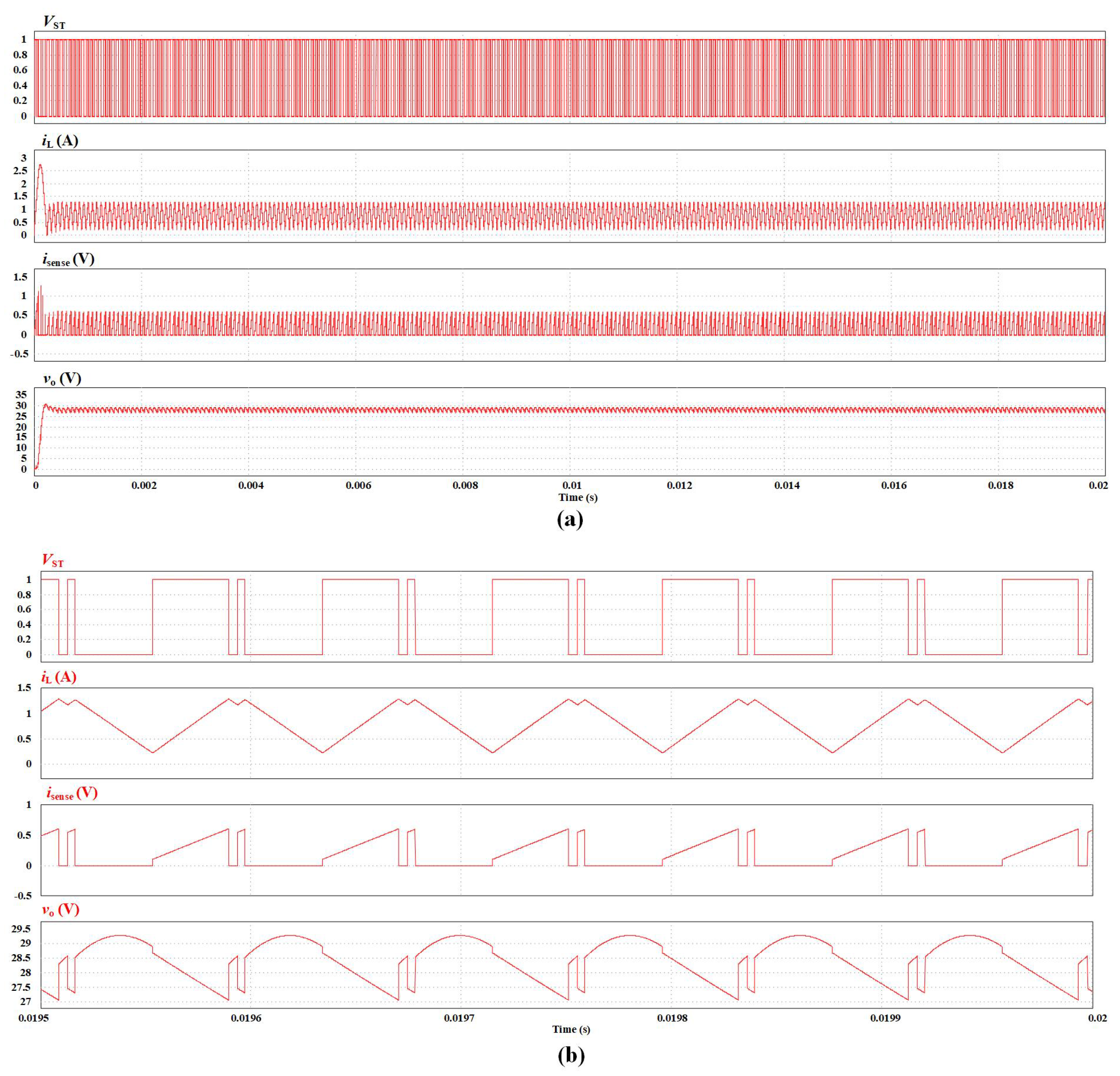
Figure 10.
In
Figure 10, from top to bottom, sub-figures correspond to the G-S voltage of power switch
, the inductor current
, the sampling value of the inductor current
(which is actually the voltage of
), and the output voltage
. One can find that, the PCMC dc-dc boost is in P-2 sub-harmonic oscillation state under the configuration of parameters. The result is also consistent with the results of bifurcation diagrams.
At last, we set the voltage dividing resistor
, the time-domain results of circuit-level simulation in PSIM software is as
Figure 11, in which sub-figures correspond to the G-S voltage of power switch
, the inductor current
, the sampling value of the inductor current
(which is actually the voltage of
), and the output voltage
from top to bottom. One can find that, the PCMC dc-dc boost is in chaotic state under the configuration of parameters. The result is also consistent with the results of bifurcation diagrams.
4.2. Experiments
In order to further validate the results of both theoretical analysis and circuit-level simulation, a simple prototype is established in this work, in which a
aluminum electrolytic capacitor is adopted as the output filtering capacitor, a type-IRF640B power MOSFET and a type-1N5008 rectifier diode are exploited as
and
of the converter, and a UC3842 IC is employed to control the dc-dc boost converter. The experiment scene is as follows:
Figure 12.
A glimpse of experiment scenes: (a) capacitance measurement scene, (b) experimental prototype.
Figure 12.
A glimpse of experiment scenes: (a) capacitance measurement scene, (b) experimental prototype.
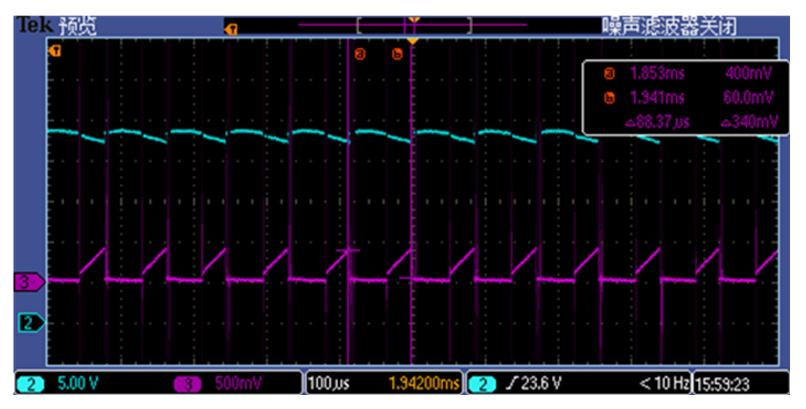
By rotating the bar of the type-3296 potentiometer on the circuit board to adjust the voltage dividing ratio, one can observe that the PCMC dc-dc boost converter experiences different nonlinear dynamic states.
Figure 13.
Experiment waveforms of P-1 stable state when the resistance of type-3296 potentiometer is around .
Figure 13.
Experiment waveforms of P-1 stable state when the resistance of type-3296 potentiometer is around .
Figure 14.
Experiment waveforms of P-2 sub-harmonic oscillation state when the resistance of type-3296 potentiometer is around : (a) time-domain waveforms, (b) enlarged peak-to-peak waveforms.
Figure 14.
Experiment waveforms of P-2 sub-harmonic oscillation state when the resistance of type-3296 potentiometer is around : (a) time-domain waveforms, (b) enlarged peak-to-peak waveforms.
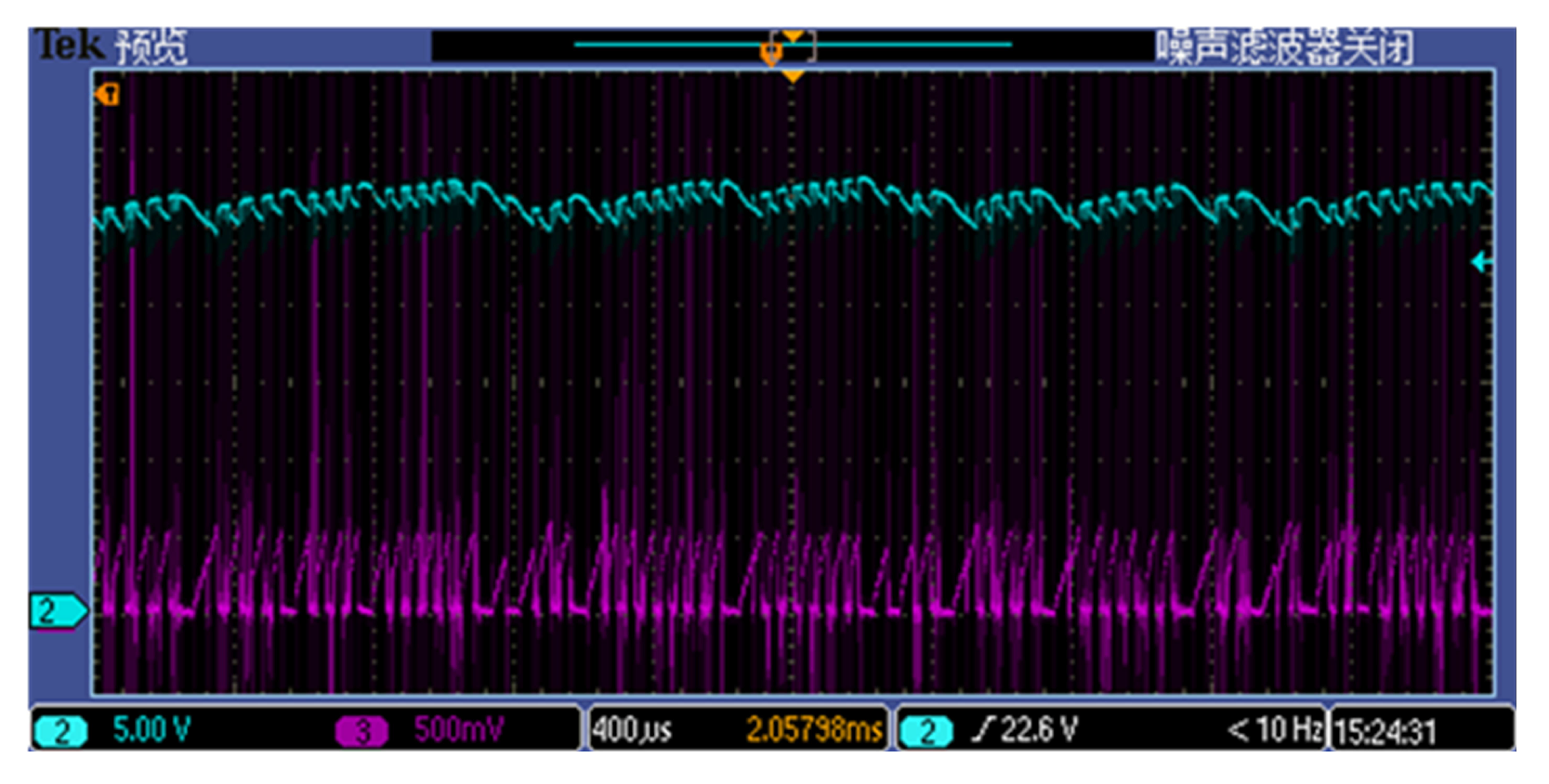
It can be found that experimental waveforms are very similar to the results of circuit-level simulation, and the variation trend is consistent with the results of bifurcation diagrams, which confirm the correctness of theoretical analysis.
5. Conclusions
The concept of fractional-order components and circuit systems has received widespread attention recently. This study appears to be the very few empirical studies on the nonlinear dynamic of real-world fractional-order circuit systems, in which the nonlinear dynamic characteristics of a real-world fractional-order system are objectively measured and evaluated, that is, a PCMC dc-dc boost converter using an aluminum electrolytic capacitor as the output filtering capacitor. Returning to the question posed at the beginning of this paper, it is now possible to state that, the fractional-order piecewise smooth model built in this work can be used for the large-signal stability analysis of the converter, by which one can draw bifurcation diagrams of the converter. The results of bifurcation diagrams emerged as reliable predictors of nonlinear dynamic analysis for the converter, when different parameters change, they can be used to predict the dynamics of the converter. Both circuit-level simulations and experiments have confirmed the correctness of the theoretical analysis. Notwithstanding the relatively limited example, this work offers a reference for the parameter selection and optimal design for power electronic converters which have fractional-order characteristics.
Figure 15.
Experiment waveforms of chaotic state when the resistance of type-3296 potentiometer is around .
Figure 15.
Experiment waveforms of chaotic state when the resistance of type-3296 potentiometer is around .
Author Contributions
Conceptualization, methodology, writing—original draft preparation, and supervision, Xi Chen; Software, validation, formal analysis, and data curation, Feng Zheng; Validation, resources, data curation, and visualization, Chao Yang; writing—review and editing, and project administration, Hui Ma; writing—review and editing, project administration, and funding acquisition, Binxin Zhu. All authors have read and agreed to the published version of the manuscript.
Funding
This research was funded by the Natural Science Project of Yichang, China (A20-3-014).
Conflicts of Interest
The authors declare no conflict of interest.
References
- Tse, C. K.; Xi, L.; Bernardo, M. D. Complex Behavior in Switching Power Converters. Proceedings of the IEEE 2002, 90(5), 768–781. [Google Scholar] [CrossRef]
- Chen, Y.; Xie, F.; et al. Improvement of Stability in a PCM-Controlled Boost Converter with the Target Period Orbit-Tracking Method. Electronics 2019, 8(12), 1432. [Google Scholar] [CrossRef]
- Chen, Y.; Zhang, B. Equivalent-Small-Parameter Analysis of DC/DC Switched-Mode Converter, 1st ed.; Springer: Singapore 189721, Singapore, 2018; pp. 1–2. [Google Scholar]
- Tse, C. K. Design-Oriented Bifurcation Analysis of Power Electronics Systems. In: In, V., Longhini, P., Palacios, A. (eds) Applications of Nonlinear Dynamics. Understanding Complex Systems.; Springer, Berlin, Heidelberg, 2009; pp. 175–187.
- Ding, L.; Wong, S. C.; Tse, C. K. Bifurcation Analysis of a Current-Mode-Controlled DC Cascaded System and Applications to Design. IEEE Journal of Emerging and Selected Topics in Power Electronics, 2020, 8(4), 3214–3224. [Google Scholar] [CrossRef]
- Aroudi, A.; Haroun, R.; et al. Fast-Scale Stability Analysis of a DC–DC Boost Converter With a Constant Power Load. IEEE Journal of Emerging and Selected Topics in Power Electronics, 2021, 8(4), 549–558. [Google Scholar] [CrossRef]
- Ji, H.; Xie, F.; et al. Small-Step Discretization Method for Modeling and Stability Analysis of Cascaded dc–dc Converters With Considering Different Switching Frequencies. IEEE Transactions on Power Electronics, 2022, 37(8), 8855–8872. [Google Scholar] [CrossRef]
- Yang, Z.; Xi, L.; Zhang, Y.; Chen, X. An Online Parameter Identification Method for Non-solid Aluminum Electrolytic Capacitors. IEEE Transactions on Circuits and Systems II: Express Briefs 2022, 69(8), 3475–3479. [Google Scholar] [CrossRef]
- Wang, K.; Sun, P.; et al. Monitoring Chip Branch Failure in Multichip IGBT Modules Based on Gate Charge. IEEE Transactions on Industrial Electronics, 2023, 70(5), 5214–5223. [Google Scholar] [CrossRef]
- Zhu, B.; Liu, Y.; et al. A Family of Bipolar High Step-Up Zeta–Buck–Boost Converter Based on “Coat Circuit”. IEEE Transactions on Power Electronics, 2023, 38(3), 3328–3339. [Google Scholar] [CrossRef]
- Zhu, B.; Huang, Y.; et al. High step-up SEPIC converters based on kinds of coat circuit. CSEE Journal of Power and Energy Systems, 2022. early access. [Google Scholar]
- Elwakil, A. Fractional-Order Circuits and Systems: An Emerging Interdisciplinary Research Area. IEEE Circuits and Systems Magazines 2010, 10(4), 40–50. [Google Scholar] [CrossRef]
- Podlubny, I. Fractional Differential Equations: An Introduction to Fractional Derivatives, Fractional Differential Equations, to Methods of their Solution and some of their Applications; Academic Press: LONDON, UK, 1998; pp. 124–125. [Google Scholar]
- Petráš, I. Fractional-Order Nonlinear Systems; Springer-Verlag: Berlin Heidelberg, 2011; pp. 43–54. [Google Scholar]
- Zhang, B.; Shu, X. Fractional-Order Electrical Circuit Theory (CPSS Power Electronics Series), 1st ed.; Springer: Singapore 189721, Singapore, 2022; pp. 39–54. [Google Scholar]
- Zhang, L.; Kartci, A.; et al. Fractional-Order Inductor: Design, Simulation, and Implementation. IEEE Access 2021, 9, 73695–73702. [Google Scholar] [CrossRef]
- Allagui, A.; Freeborn, T. J.; Elwakil, A. S.; et al. Review of fractional-order electrical characterization of supercapacitors. Journal of Power Sources 2018, 400, 457–467. [Google Scholar] [CrossRef]
- Chen, X.; Pei, M. Enhancing parameter identification of electrochemical double layer capacitors by fractional-order equivalent impedance models and Levy flight strategy. International Journal of Circuit Theory and Applications 2022, online. [Google Scholar] [CrossRef]
- Zou, C.; Zhang, L.; et al. A review of fractional-order techniques applied to lithium-ion batteries, lead-acid batteries, and supercapacitors. Journal of Power Sources 2018, 390, 286–296. [Google Scholar] [CrossRef]
- Huang, Y.; Chen, X. A fractional-order equivalent model for characterizing the interelectrode capacitance of MOSFETs. IEEE COMPEL - The international journal for computation and mathematics in electrical and electronic engineering 2022, 41(5), 1660–1676. [Google Scholar] [CrossRef]
- Allagui, A.; Elwakil, A. S.; Fouda, M. E. Revisiting the Time-Domain and Frequency-Domain Definitions of Capacitance. IEEE Transactions on Electron Devices 2021, 68(6), 2912–2916. [Google Scholar] [CrossRef]
- ONSENMI, UC3842B: High Performance Current Mode Controllers. Available online: https://www.onsemi.com/pdf/datasheet/uc3842b-d.pdf (accessed on 22 Feb. 2023).
- Chen, X.; Xi, L.; et al. Fractional techniques to characterize non-solid aluminum electrolytic capacitors for power electronic applications. Nonlinear Dynamics 2019, 98, 3125–3141. [Google Scholar] [CrossRef]
- Diethelm, K. The Analysis of Fractional Differential Equations: An Application-Oriented Exposition Using Differential Operators of Caputo Type; Springer-Verlag: Berlin Heidelberg, 2010; pp. 195–225. [Google Scholar]
- Chen, X.; Chen, Y. A Modeling and Analysis Method for Fractional-order DC-DC Converters. IEEE Transactions on Power Electronics 2017, 32(9), 7034–7044. [Google Scholar] [CrossRef]
- Oustaloup, A.; Levron, F.; et al. Frequency-band complex noninteger differentiator: Characterization and synthesis. IEEE Transactions on Circuits and Systems I-Fundamental Theory and Applications 2000, 47(1), 25–39. [Google Scholar] [CrossRef]
- Xue, D.; Chen, Y. System Simulation Techniques with MATLAB® and Simulink®, 1st ed.; John Wiley Sons: West Sussex, United Kingdom, 2013; pp. 85–90. [Google Scholar]
- Malti, R.; Victor, S.; et al. CRONE Toolbox for system identification using fractional differentiation models. IFAC-Papers OnLine 2015, 48(28), 769–774. [Google Scholar] [CrossRef]
- Zhang, Y.; Lian, Z.; et al. An ESR Quasi-Online Identification Method for the Fractional-Order Capacitor of Forward Converters Based on Variational Mode Decomposition. IEEE Transactions on Power Electronics 2022, 37(4), 3685–3690. [Google Scholar] [CrossRef]
|
Disclaimer/Publisher’s Note: The statements, opinions and data contained in all publications are solely those of the individual author(s) and contributor(s) and not of MDPI and/or the editor(s). MDPI and/or the editor(s) disclaim responsibility for any injury to people or property resulting from any ideas, methods, instructions or products referred to in the content. |
© 2023 by the authors. Licensee MDPI, Basel, Switzerland. This article is an open access article distributed under the terms and conditions of the Creative Commons Attribution (CC BY) license (http://creativecommons.org/licenses/by/4.0/).
