Preprint
Article

Applying Stamping Without Die to Micro-hole Array Processing

Altmetrics

Downloads

119

Views

33

Comments

0

This version is not peer-reviewed

Submitted:

18 April 2023

Posted:

19 April 2023

You are already at the latest version

Alerts
Abstract
Aluminum alloy (Al6061) sheet micro-hole processing is extensively used in smartphones, tablet PC, and smart wearable devices. The micro-hole processing is commonly performed using laser, micro drilling, microstamping, micro discharge, and chemical etching technologies. Micro-stamping technology is characterized by precision and rapid processing, but the precision positioning of the punch head and lower die is one of the major difficulties in micro-hole stamping, especially in manufacturing array micro-holes. This study used stamping without die technology. This technology uses an array punch head to punch the lower die holes on the base, then performs array micro-hole stamping. The experimental results show that a micro-hole array with 37 micro-holes were successfully manufactured and can be reproduced many times. Tapered array micro-holes with a high aspect ratio can be manufactured using this stamping without die technology; the micro-hole depth can be 260μm, the inlet diameter is 116μm, and the outlet diameter is 25μm. This study has successfully developed the feasibility of array micro-hole stamping technology.
Keywords: 
Subject: Engineering  -   Industrial and Manufacturing Engineering

1. Introduction

Micro-hole processing can process different shapes, such as circles, triangles, rectangles, and polygons. The hole-wall can be upright, tapered, or curved. Currently, the laser is extensively used for micro-hole processing in industrial circles. The laser can process various micro-hole shape. A circular hole is the most familiar micro-hole shape. The upright circular hole and tapered hole processing methods are available according to the hole wall patterns. For straight-hole processing, conventional processing technologies include micro-drilling, micro-milling, and stamp-forming [1,2]. Regarding tapered hole processing, the common processing technologies include electroforming, electrical discharge machining, etching, and laser [3,4,5].
The aluminum alloy sheet micro-holes are extensively used in intelligent electronic devices, such as notebook computers, smartphones, tablet PC, and intelligent wearable devices. These micro-holes are usually used for special functions, such as microperforation illumination. Generally, microperforation illumination of less than 100 μm is required. Currently, machine and laser drilling are common methods used in industrial circles. Machine drilling is less efficient and only workable for vertical sidewalls. In contrast, tapered sidewalls can provide better backlight projection efficiency. The sheet can be drilled rapidly to make tapered sidewalls with laser drilling. The picosecond laser or femtosecond laser is used extensively. These methods are expensive, and the material removal rate is very low [6].
This study proposed manufacturing array micro-holes using stamping without die concept [7] and used the punch head Reverse-EDM method [8,9]. This method can directly punch micro-holes on the aluminum alloy sheet without a complicated mold for precision positioning. In addition, the punch head is not worn too much after stamping. The stamping angle and depth can control the inlet and outlet sizes of micro-holes.
A micro-stamping mechanism is designed in this study, as shown in Figure 1. The equipment is an engraving EDM (Sodick AP1L). An annular array of circular holes are drilled in the brass electrode in the array punch head processing method. Excess materials are removed by reverse discharge, and the micro-hole profile on the electrode is reproduced to make an array punch head. As shown in Figure 1 (a), the array punch head performs the stamping forming of the lower die holes. As shown in Figure 1 (b), the sample is fixed to the lower die holes during stamping and to the mold by vacuum adsorption. This stamping method can perform continuous stamping by changing the sample, and implementing rapid processing without precision positioning.

2. Materials and Methods

The array micro-holes were tested. The mechanism design for the experiment is shown in Figure 2. The machinery equipment is an engraving EDM (Sodick AP1L). The XYX three-axis displacement accuracy can be 0.1 μm. First, the lower die holes were directly stamped by the punch head in the lower die. The stamping sample was placed on the lower die holes and fixed by vacuum adsorption. The lower die is made of an aluminum alloy (Al5052), a soft alloy. The punch head directly punches it at a stamping depth of 100 μm. After the lower die stamping, it is placed on the lower die holes and fixed by vacuum adsorption. As the punch head only moves on the Z-axis, the concentric position of the punch head and the lower die holes can be maintained. In the subsequent micro-stamping process, as long as the vacuum pump is depressurized, a new sample can be placed for the next stamping.

2.1. Design of experiments

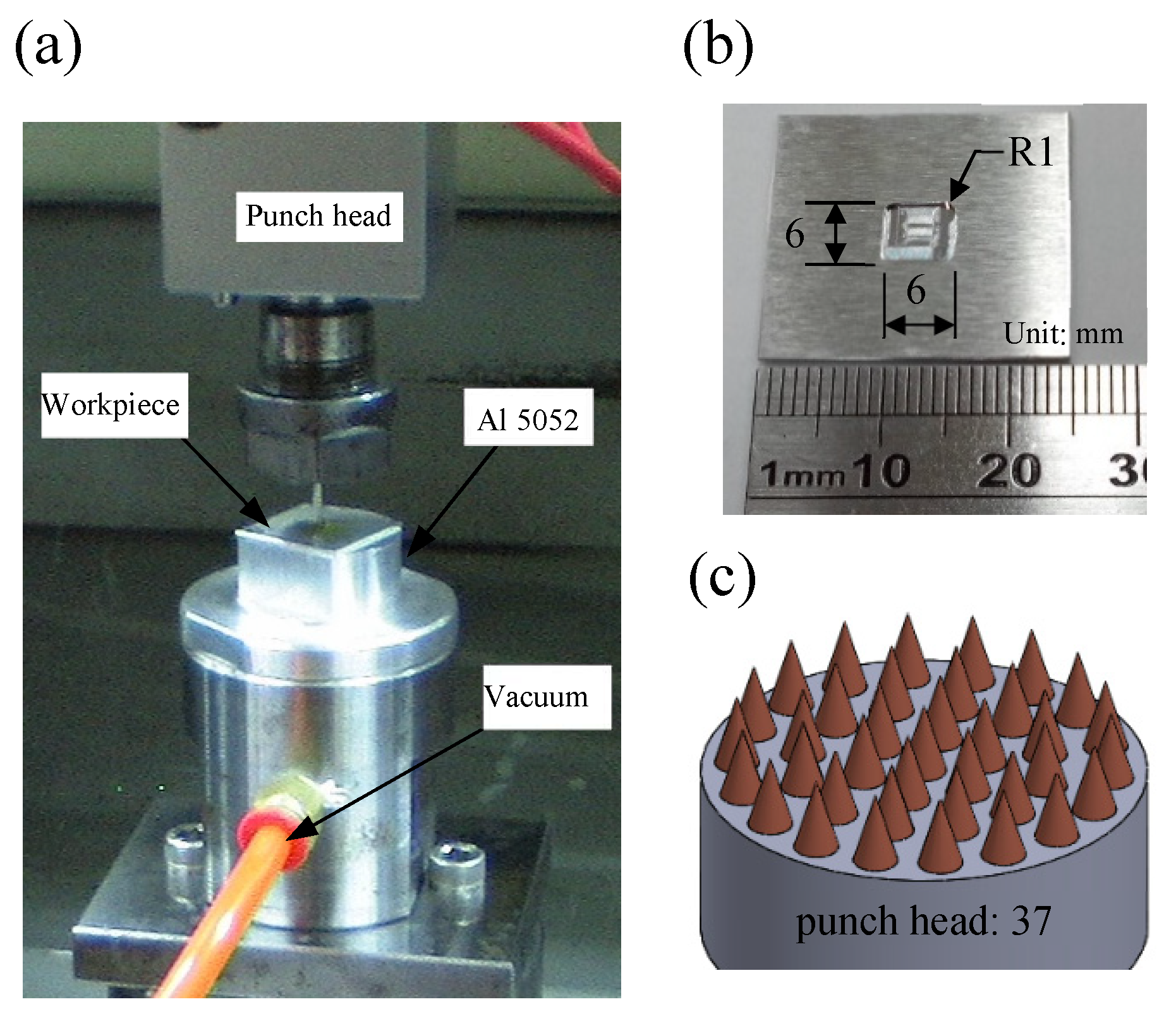
The main objective of this experiment is to process the micro-hole array. First, the lower die holes are stamped in the lower die. Afterward, the stamping sample is fixed to the lower die by vacuum adsorption. As shown in Figure 2(a), when the sample is fixed by vacuum, the punch head only moves on the Z-axis. The lower die is made of aluminum alloy (Al5052), a soft alloy. It can be directly stamped by the punch head. The stamping depth is 100 μm. After stamping, the lower die is placed on lower die holes and fixed by vacuum adsorption. The punch head only moves on the Z-axis, and the concentric position of the punch head and lower die holes can be maintained. During microstamping, as long as the vacuum is relieved, a new sample can be placed for the next stamping.
As shown in Figure 2. (b), the size of the stamping sample is 25×25×1 mm, the size of the center milling groove is 6×6 mm, the depth is 0.74 mm, and the sample thickness is 0.26 mm (260 μm). In the microstamping process, it is difficult to accurately locate the punch head and lower die holes [10,11]. Therefore, this study used a structure combining the lower die holes with vacuum adsorption. The lower die holes were made using the punch head to stamp the lower die directly. The punch stroke setting mode was similar to peck drilling, and reciprocating progressive stamping was adopted. The punch head is a ø2 mmWC round bar with 37 microneedles, as shown in Figure 2. (c).

2.2. Punch head manufacturing

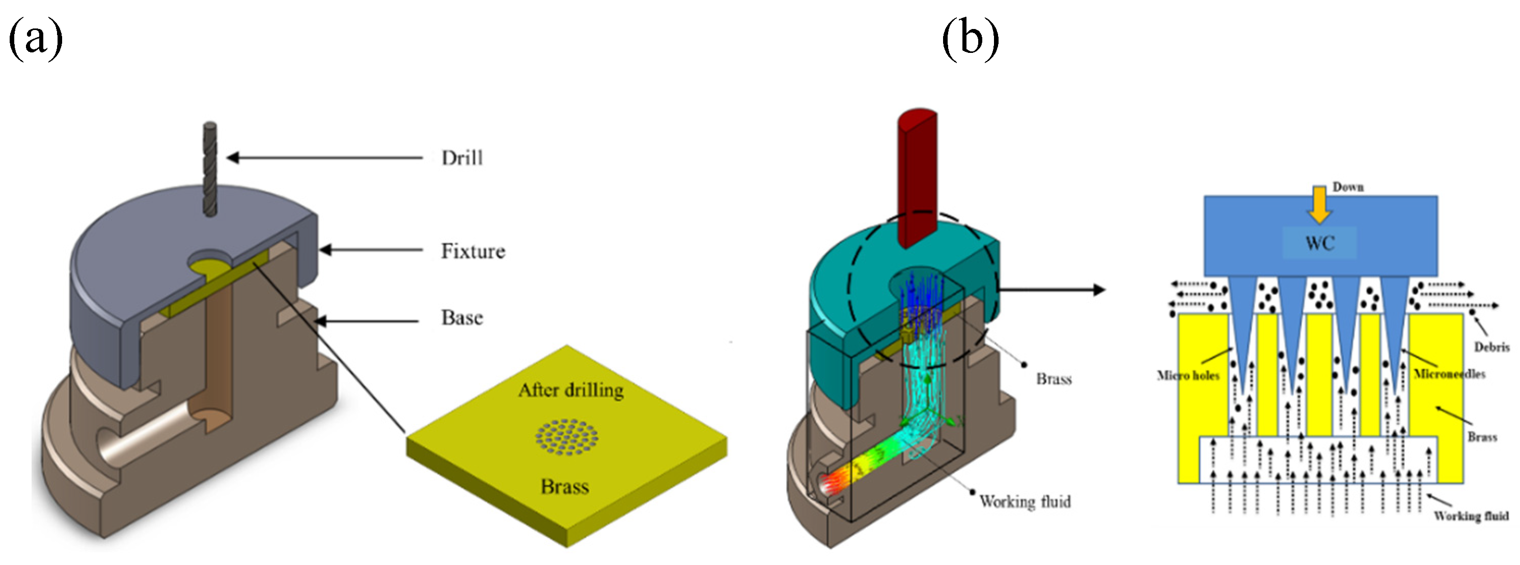
As shown in Figure 3 (a), the micro punch head used in this study is formed by Reverse-EDM. The microhole electrode for EDM is made of 25×25×1 mm brass material. There are 37 holes with a diameter of 140 μm. In the drilling process, the brass electrode is fixed by a self-made fixture. A high-speed spindle and micro drill bit are fixed to the spindle of the electrical discharge machine by 3R SYSTEM for drilling. The cooling fluid is the working fluid of the electrical discharge machine. There is a ø8 mm channel in the base of the fixture for the brass sample has two major functions. First, the bottom of the drilling sample is a hollow structure, and the channel is available for perforation processing. Second, in the EDM process, the channel acts as the channel for the bottom cooling fluid.
As shown in Figure 3 (b), the second step is to connect the bottom of the channel to the brass electrode after drilling. In the EDM process, the working fluid flows from the bottom into the gap between the WC and brass electrode to remove the debris and implement stable and efficient EDM. The working fluid flows through the bottom channel into the discharge region between the WC electrode and the brass. The micro-hole array channel can spray a lot of working fluid more efficiently than a single-hole. A large amount of debris and gas produced by micro-drilling can be removed effectively. The electrode (WC) is fed downwards in the Z direction. The feed path is in tapered dynamic tracking mode. The three parameters, Z (depth), R (major diameter), and Q (minor diameter) of the tapered dynamic tracking mode, are set up. The discharge depth (Z) is set up to achieve the punch head length of 500μm. According to the test results, the discharge depth is about 750 μm. The shaking radius of Q is set as 1μm.
This section aims to produce an annular array micro punch head. Reverse-EDM is a high-accuracy machining method. Its forming process is influenced by multiple factors, such as the discharge circuit, the magnitude of current, discharge time, off time, discharge depth, and shaking radius. These factors can influence the shape of the micro punch head. Therefore, the micro-hole array is drilled in the brass sample (C2680) using a high-speed spindle. The required array punch head is formed using a Ø2 mm WC for reverse discharge. As the micro-hole array is an annular array, the produced punch heads are arranged in an annular array fashion. As shown in Figure 2 (c), the number of annular array micro punch heads is 37.
According to the parameter selection shown in Table 1, this section aims to discuss the feasibility of Reverse-EDM. Therefore, two modes of discharge circuit are selected: Generator Mode (GM) and Servo Feed (SF). The GM circuit is one of the most fundamental circuits in EDM, which uses a voltage pulse to generate discharge. It is suitable for rapidly processing simple geometric shapes. The SF circuit is developed from the GM circuit, which achieves higher machining accuracy and more complicated geometric shapes by controlling the motion of the discharge electrode [12,13]. In this study, the minimum discharge energy is selected for GM and SF circuit experiments. A current of 0.1A, discharge time of 6μs, and off time of 24 μs were selected for the GM circuit. The capacitance of 1000 pF and shaking radii of 70 μm and 80μm were selected for the SF circuit. This study aims to further understand the influence of different parameters on EDM from this experiment. It also aims to determine the optimum parameter combination for implementing efficient and high-precision machining.
For the convenience of subsequent experimental discussion, three micro punch heads are represented by the abbreviations of the circuit and initial shaking radius, respectively. To be specific, Experiment I: GM-R70; Experiment II: SF-R70; Experiment III: SF-R80. This naming method helps simplify the experimental records and improve the readability of experimental data. It is convenient for comparing different experimental results.
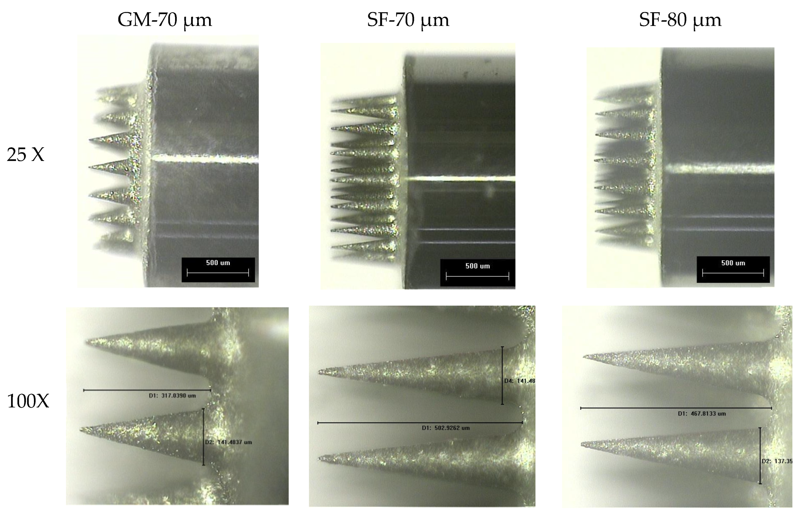
According to Figure 4, the profile of the array punch head after Reverse-EDM is observed. Due to the different discharge parameters of the three micro punch heads, there are differences in the profile of the punch head and machining time. The main discharge circuits of GM-R70 μm and SF-R70μm are different, but the discharge depth and shaking radius are the same. They use the same minimum discharge energy, so the difference in machining time is only 57 sec. However, the difference in the average length of the punch heads is 182 μm, i.e., 52%. The difference between the main initial shaking radii of SF-R70μm and SF-R80μm is 10 μm. The larger the shaking radius, the greater the influence on the overcut phenomenon at the front end of the punch head. Compared to SF-R70 μm, the average length of punch heads of SF-R80 μm is shortened by about 8.1%, which is 464 μm. The array micro punch head consists of 4 annular arrays, and each punch head has a similar appearance.
Measuring each punch head, especially the inner annular micro punch head, is difficult. Samples are used to simplify the analysis. The micro punch head is fixed to a cubic material by an ER collet. The material has 4 faces: I, II, III, and IV. By placing it on the 4 faces, 4 circumferential surfaces of the micro punch head can be observed. One micro punch head in the middle of each array is selected as the measurement sample. Four micro punch heads are taken from each array for analysis, including punch length, angle, and root diameter.
As shown in Figure 4, according to the observation through OM at magnifications of 25 times and 100 times, the micro punch head profile after reverse discharge shows high replicability. Each punch head of the array has the same shape. After processing, the GM-70 μm and SF-70 μm micro punch heads have the same discharge depth, shaking radius, and root diameter. This is due to the difference in energy consumption induced by different discharge circuits. A shorter length of the GM-70 μm micro punch head results in a larger punch angle.
According to the results shown in Figure 5 (a), the lengths of micro punch heads are measured. The minimum, average, and maximum lengths of SF-70 μm are 503 μm, 505 μm, and 508 μm, respectively. The difference is less than 1%. The minimum, average, and maximum lengths of SF-80 μm are 450 μm, 460μm, and 468 μm with a difference of 4%. The average length of GM-70 μm is 328 μm. It is the shortest punch head, but the difference among the punch heads is about 6.9%. According to the experimental results, the micro array punch head made by reverse discharge has high replicability of punch length, and SF is more suitable than GM. As shown in Figure 5, the image measurement system of OM is used for the geometric measurement of punch angle. In the measurement results of four faces, the maximum error of the punch angle is less than 1%. The punch heads manufactured by SF-70 μm have the minimum punch angle, and the average angle is 14.2°.

2.3. Stamping experiment

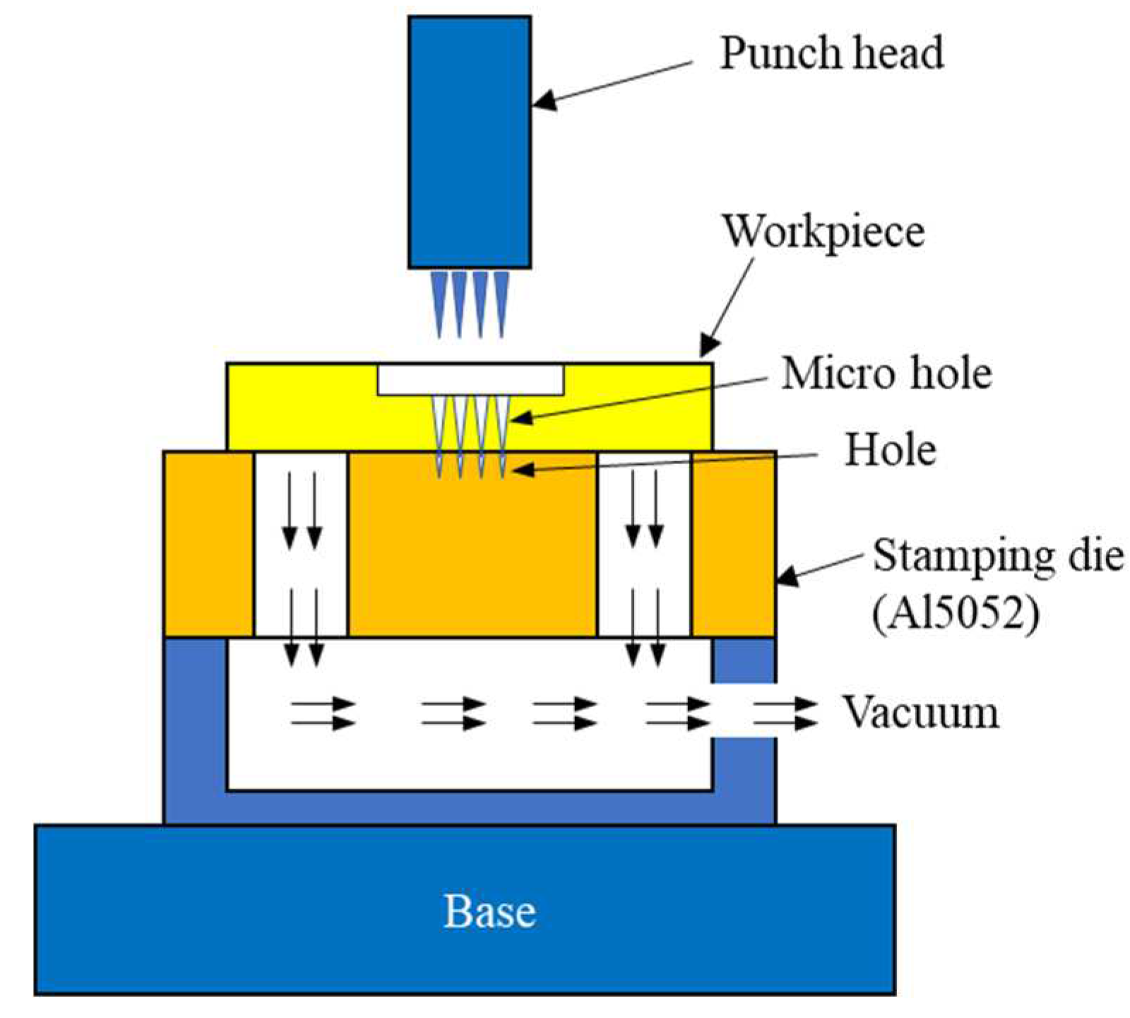
As shown in Figure 6, the lower die used in this study is an aluminum alloy (Al 5052). The lower die holes are designed in a vacuum adsorption structure. The punch head directly stamps the lower die to make the required die holes. The punch stroke setting, similar to peck drilling, is used for lower die holes, reciprocating progressive stamping. Each punch stroke is 0.01 mm, the feedrate is 0.5 mm/min, and the stamping depth is 120 μm.
As shown in Table 1, this study uses the same punch head (SF-R70) to perform stamping forming of 50 identical Al6061 samples. In the experiment, the aluminum sheet (Al 6061-T651) is milled to the required size. Then the annular array punch head with 37 micro-shafts completed by Reverse-EDM is used for stamping. The sample stamping method is the same as the lower die hole forming method, but the stamping depth is 350 μm.
Table 2. Stamping parameters.
Sample Sample thickness Punch angle Stamping speed Quantity of microholes Stamping depth Stamped quantity
Al6061 260μm 15.8° 0.5mm/min 37 350 μm 50 pcs

3. Results and discussion

3.1. Sample inlet and outlet

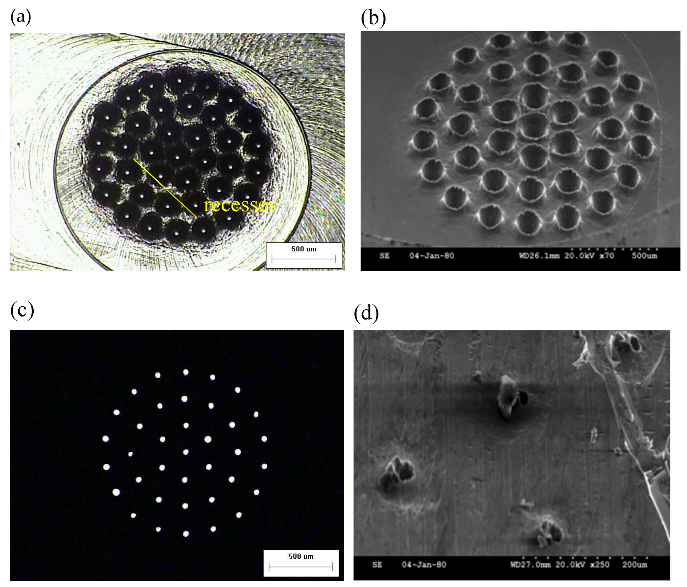
As shown in Figure 7 (a)(b), array micro-hole inlet profile after stamping is observed through OM. Clustered bulges formed at the inlet as the material was compressed. The raised areas between holes overlap each other, resulting in wrinkles. The inlet and outlet diameters of the sample were measured, and the average and tolerance values were calculated. Based on the results, the maximum value of the inlet diameter is 137 μm, the minimum value is 127 μm, and the average diameter is 133 μm. The array micro-hole profile is observed through SEM. There are apparent wrinkles at the inlet due to the extrusion between the holes. The height of the bulge is more evident than that of single-hole stamping.
As shown in Figure 7 (c), the array micro-hole outlet profile is observed by OM backlight projection. The light transmission at the outlet can be observed clearly. It is observed in the partially enlarged outlet view that the outlet’s roundness is not ideal. An ellipse is presented, and annular extrusion occurs around the inlet. The diameters of all outlets are measured. The maximum value is 41 μm, the minimum value is 29 μm, and the average diameter is 36 μm. The result of the outlet diameter matches the original experimental goal. As shown in Figure 7 (d), there are annular recesses and obvious puncture bulges around the outlet. The main reason is that in the stamping process, the lower die is formed by stamping, and the lower die hole inlet will be raised. When the sample is fixed on the lower die holes and stamped, the sample outlet is extruded by the raised area of lower die holes, leading to recesses around the sample outlet [14,15].
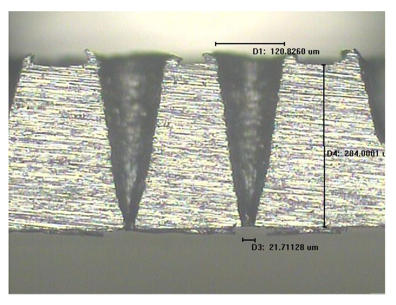
As shown in Figure 8, the last stamping sample is processed as follows: first, it is cut using the EDM. Then its section is ground using an automatic finishing machine to observe the profile of the tapered hole. In the stamping process, under the effect of the lateral force around the tapered hole inlet, the holes extrude each other, leading to a steep inlet end. This extrusion effect results in a bulge height of about 40μm. The annular micro-hole array has the same tapered micro-hole structure, and the same structure can be replicated.

3.2. Punch head surface analysis

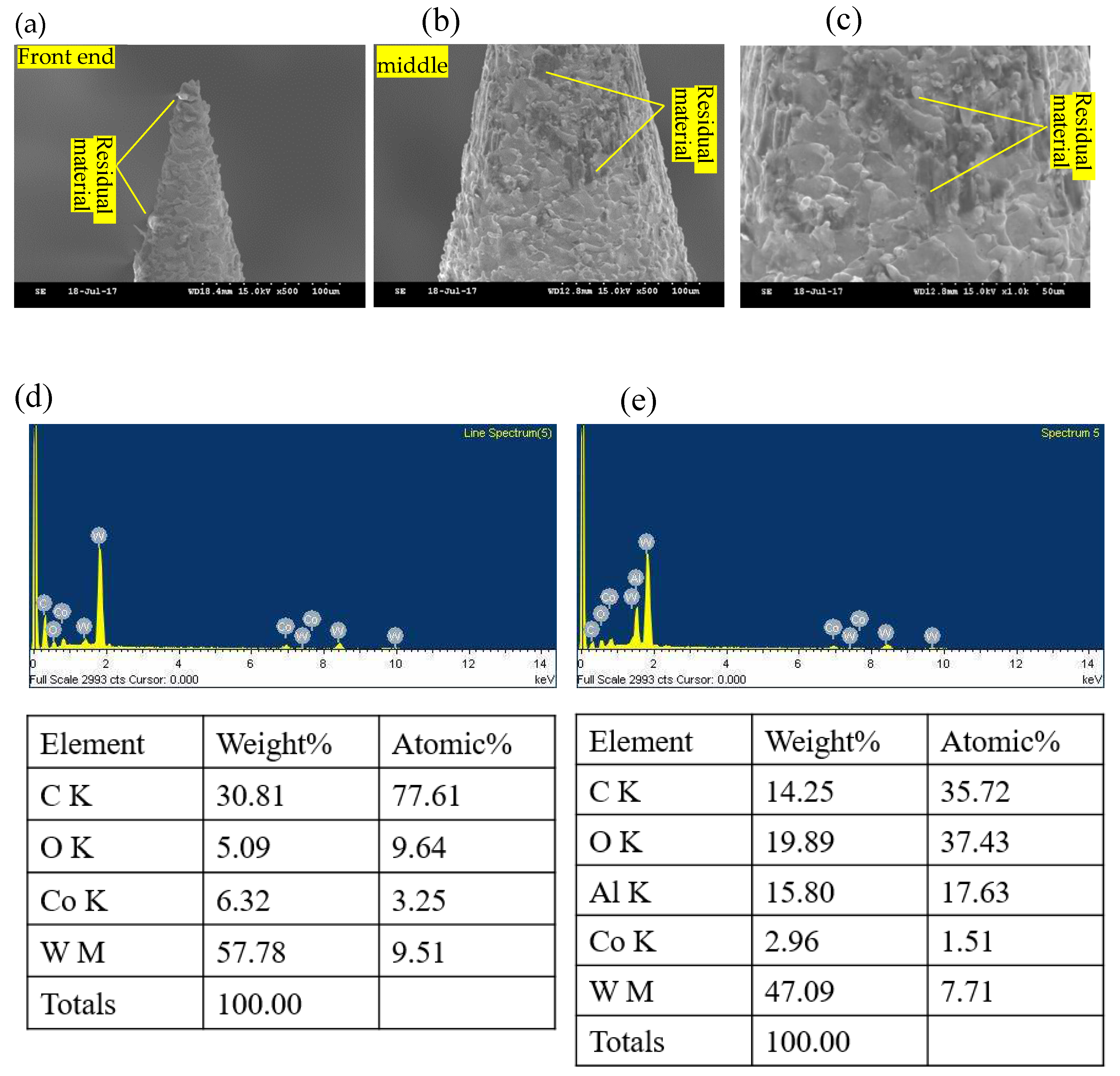
As shown in Figure 9 (a)(b)(c), in the micro punch head stamping process, there are extrusion and friction between the sample and the punch head. SEM analysis shows no obvious fracture or wear on the surface of the punch head. However, residual material-like traces on the surface of the punch head are present. To clarify whether sample material is adhering to the surface of the punch head, elemental analysis is performed for the surface of the punch head before and after stamping.
As shown in Figure 9 (d)(e), the punch head surface before and after stamping is analyzed by using EDS (Energy-dispersive X-ray spectroscopy). Five points are sampled to analyze the elemental composition. It is observed that after stamping, the punch head surface has Al element in five measurements. Al element is in frictional grip on the punch head surface, not the general bonding of metal atoms. The metal element may drop off due to the ultrasonic oscillation in the cleaning process. Therefore, there are significant differences in the Al element. However, it can be confirmed in the test result that there will be residual Al element on the punch head surface in the stamping process. Only a residual Al element was observed in the Figureures. There is no film-like layer.
Reference [16] can be obtained from document analysis. At the high temperature in the EDM process, the WC hard alloy is decomposed into other elements. After the WC reacts with O, the WC is decomposed into alloy elements, such as C, Co, and W. Firstly, it can be observed that there is no obvious change in the weight percentages of O, Co, and W before and after stamping. However, the C element is reduced. Obviously, the average C is about 24.5% before stamping and 17.4% after stamping. It is reduced by about 7.1%. However, the average Al element is about 8.1%. The friction may decrease in this stamping process, and the C increases the Al element.

3.3. Sample surface grinding

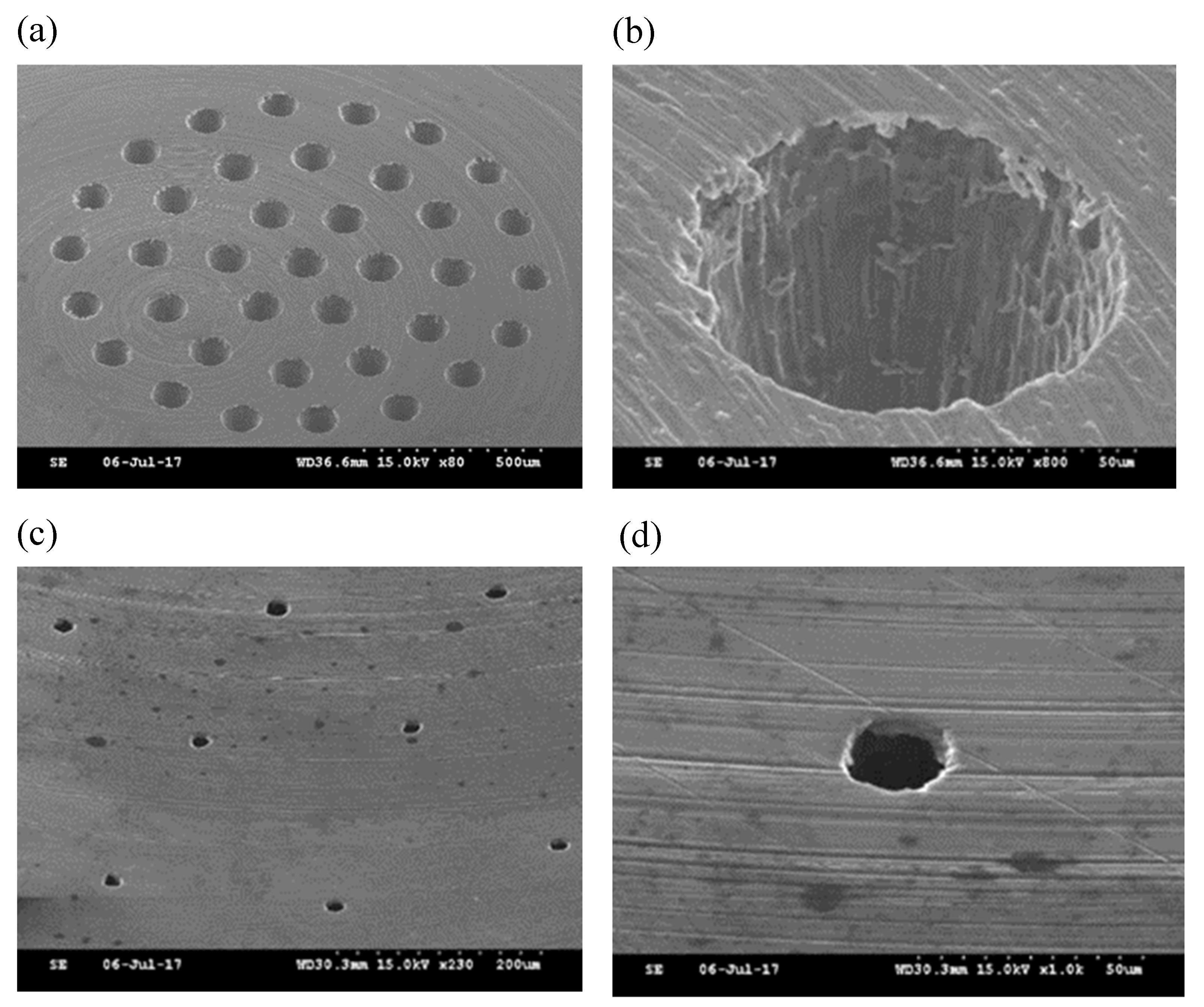
According to the experimental results, the inlet of the micro-bulges under the effect of extrusion in the stamping process. The outlet forms convex and concave profiles due to the puncture of the punch head. To overcome this problem, a Ø3 mm grinding rod is used with #2000 sandpaper. The inlet and outlet grinding depths are set at 40 μm and 30 μm, respectively. The surfaces of the microhole before and after grinding were compared. The result shows that a smooth micro-hole inlet and outlet can be obtained effectively by grinding with a good surface profile. Additionally, the grinding mode can effectively solve the inconsistent diameter defect resulting from an incomplete tear of the micro-stamping outlet.
As shown in Figure 10, the defective appearance resulting from the puncture is solved effectively after grinding the microhole. Bulge, recess, and incomplete tear defects are present at the inlet and outlet before grinding. The defects in the inlet can be removed effectively after grinding with local burrs at the outlet. As the outlet burrs are small, they converge towards the hole wall. The micro-hole inlet and sample surface on the same plane can be obtained by grinding with a good surface profile. Additionally, the problem of inconsistent diameter resulting from incomplete tear of micro-stamping outlet can be solved effectively by grinding [17,18].
To analyze the influence of grinding on the size of microholes, the microholes were sampled and measured. For convenient sample analysis, there are 37 holes encoded, including three circles of annular array microholes (from inside to outside) and one center hole. The effective samples include the center hole, 2 holes from the first circle, and 3 holes from the second and third circles, respectively. There are 9 holes in all.
Figure 11 shows the measurement results of the inlet diameter before and after grinding. It is observed that the inlet diameter curve before grinding has significant fluctuations. Whereas the inlet diameter curve after grinding shows a relatively stable trend. The maximum inlet diameter before grinding is 187 μm, the minimum is 121 μm, and the average value is 153 μm. It can be observed that the inlet diameter at the center is the largest (No.1). The inlet diameters of the three microholes of the third circle are the minimum value (No.37) with fluctuations. It may be because of the raised areas. The inlet diameter can validate this measurement result after grinding. The maximum value of inlet diameter after grinding is 125 μm, the minimum value is 106 μm, the average value is 116 μm, and the linear variation trend of the diameter is the same as before grinding.
According to the observation on the outlet diameter, the maximum diameter value before grinding is 44 μm, the minimum value is 29 μm, and the average value is 37 μm. Tears and recessions at the outlet can cause significant errors in outlet measurement. Therefore, the outlet diameter is measured after grinding. According to the measurement results, the maximum value of the outlet diameter is 28 μm, the minimum value is 22 μm, and the average value is 25 μm. According to the linear trend of outlet diameter, the center has the maximum value, and the outlet diameter is smaller at the outermost circle. This diameter variation trend is the same as the inlet diameter, except for the sudden drop of No. 5. sample 19.5 μm of the first circle, the trend is approximately identical with the inlet.

4. Conclusions

This study used Reverse-EDM to manufacture array punch heads, and used stamping to manufacture a micro-hole array. In addition, the required dimensions of the array punch heads can be manufactured by the Reverse-EDM. The following conclusions are made:
  • The sample is adsorbed by vacuum, and the sheet and nonmagnetic materials can be milled effectively. This method is applicable to clamping stamping samples.
  • The lower die holes are directly formed by stamping. The precision positioning problem of the punch head and lower die can be overcome. The microholes are punched by tapered punch heads. Finally, it is used in the micro stamping of Al6061 sample. The tapered microhole stamping forming is implemented successfully. The average inlet and outlet diameters of tapered microholes are 128 μm and 36 μm, respectively.
  • There are 37 array punch heads used in this study. The brass electrode can be produced by reverse discharge in the future. Elastic design can be used to meet the required size and quantity of the products, hoping to meet different needs.
  • The problems caused by inlet bulge, incomplete tear of outlet and bulge defects often occur in the micro stamping process. To effectively remove the inlet bulge defect, a high-speed spindle is combined with a grinding rod to grind the sample surface. Different models of sandpaper can be selected, such as #240, #1000 and #2000. A larger the sandpaper model has lower surface roughness value Ra. The average Ra value after grinding with #2000 sandpaper is 0.565. Finer sandpaper will be used for grinding in the future, the Ra value is expected to be further increased.

References

  1. Hourmand, M., Sarhan, A. A. D., & Yusof, N. M. (2017). Development of new fabrication and measurement techniques of micro-electrodes with high aspect ratio for micro EDM using typical EDM machine. Measurement, 97, 64-78. [CrossRef]
  2. Yin, Q. F., Wang, B. R., Zhang, Y. B., Ji, F., & Liu, G. M. (2014). Research of lower tool electrode wear in simultaneous EDM and ECM. Journal of Materials Processing Technology, 214(8), 1759-1768. [CrossRef]
  3. Perez-Diaz, O., & Quiroga-Gonzalez, E. (2020). Silicon Conical Structures by Metal Assisted Chemical Etching. Micromachines, 11(4), Article 402. [CrossRef]
  4. Zhang, J. Z., Ming, P. M., Zhang, X. M., Qin, G., Yan, L., Zhao, X. K., & Zheng, X. S. (2020). Facile Fabrication of Highly Perforated Hollow Metallic Cylinder with Changeable Micro-Orifices by Electroforming-Extrusion Molding Hybrid Process. Micromachines, 11(1), Article 70. [CrossRef]
  5. Zhanwen, A., Chen, L. L., Wu, Y., Du, R. B., Bai, H. L., & Zou, G. S. (2021). Controlling of Diameter and Taper in Ultrafast Laser Helical Drilling. Chinese Journal of Lasers-Zhongguo Jiguang, 48(8), Article 0802017. [CrossRef]
  6. Chang, Y. J., Hung, Y. C., Kuo, C. L., Hsu, J. C., & Ho, C. C. (2017). Hybrid stamping and laser micromachining process for micro-scale hole drilling. Materials and Manufacturing Processes, 32(15), 1685-1691. [CrossRef]
  7. Hung, Y. C., Chang, Y. J., Kuo, C. L., Hsu, J. C., & Ho, C. C. (2016). Comparison between Laser and Stamping without Die (SWD) for Micro Tapered Hole Forming. Applied Sciences-Basel, 6(3). [CrossRef]
  8. Hwang, Y. L., Kuo, C. L., & Hwang, S. F. (2010). Fabrication of a micro-pin array with high density and high hardness by combining mechanical peck-drilling and Reverse-EDM. Journal of Materials Processing Technology, 210(9), 1103-1130. [CrossRef]
  9. Talla, G., Gangopadhyay, S., & Kona, N. B. (2017). Experimental investigation and optimization during the fabrication of arrayed structures using reverse EDM. Materials and Manufacturing Processes, 32(9), 958-969. [CrossRef]
  10. Xu, J., Guo, B., Shan, D. B., Wang, C. J., Li, J., Liu, Y. W., & Qu, D. S. (2012). Development of a micro-forming system for micro-punching process of micro-hole arrays in brass foil. Journal of Materials Processing Technology, 212(11), 2238-2246. [CrossRef]
  11. Yu, Z. Y., Li, D. P., Yang, J. F., Zeng, Z. J., Yang, X. L., & Li, J. Z. (2019). Fabrication of micro punching mold for micro complex shape part by micro EDM. International Journal of Advanced Manufacturing Technology, 100(1-4), 743-749. [CrossRef]
  12. Hourmand, M., Sarhan, A. A. D., & Yusof, N. M. (2017). Development of new fabrication and measurement techniques of micro-electrodes with high aspect ratio for micro EDM using typical EDM machine. Measurement, 97, 64-78. [CrossRef]
  13. Yin, Q. F., Wang, B. R., Zhang, Y. B., Ji, F., & Liu, G. M. (2014). Research of lower tool electrode wear in simultaneous EDM and ECM. Journal of Materials Processing Technology, 214(8), 1759-1768. [CrossRef]
  14. Funazuka, T., Dohda, K., Shiratori, T., Hiramiya, R., & Watanabe, I. (2021). Effect of Punch Surface Grooves on Microformability of AA6063 Backward Microextrusion. Micromachines, 12(11), Article 1299. [CrossRef]
  15. Wang, X., Zhang, D., Gu, C. X., Shen, Z. B., & Liu, H. X. (2014). Research on the Micro Sheet Stamping Process Using Plasticine as Soft Punch. Materials, 7(6), 4118-4131. [CrossRef]
  16. Gu, W. H., Jeong, Y. S., Kim, K., Kim, J. C., Son, S. H., & Kim, S. (2012). Thermal oxidation behavior of WC-Co hard metal machining tool tip scraps. Journal of Materials Processing Technology, 212(6), 1250-1256. [CrossRef]
  17. Processes: A Comprehensive Review. Nanomaterials, 12(23), Article 4214. [CrossRef]
  18. Wang, Q. Y., Vohra, M. S., Bai, S. W., & Yeo, S. H. (2021). Rotary ultrasonic-assisted abrasive flow finishing and its fundamental performance in Al6061 machining. International Journal of Advanced Manufacturing Technology, 113(1-2), 473-481. [CrossRef]
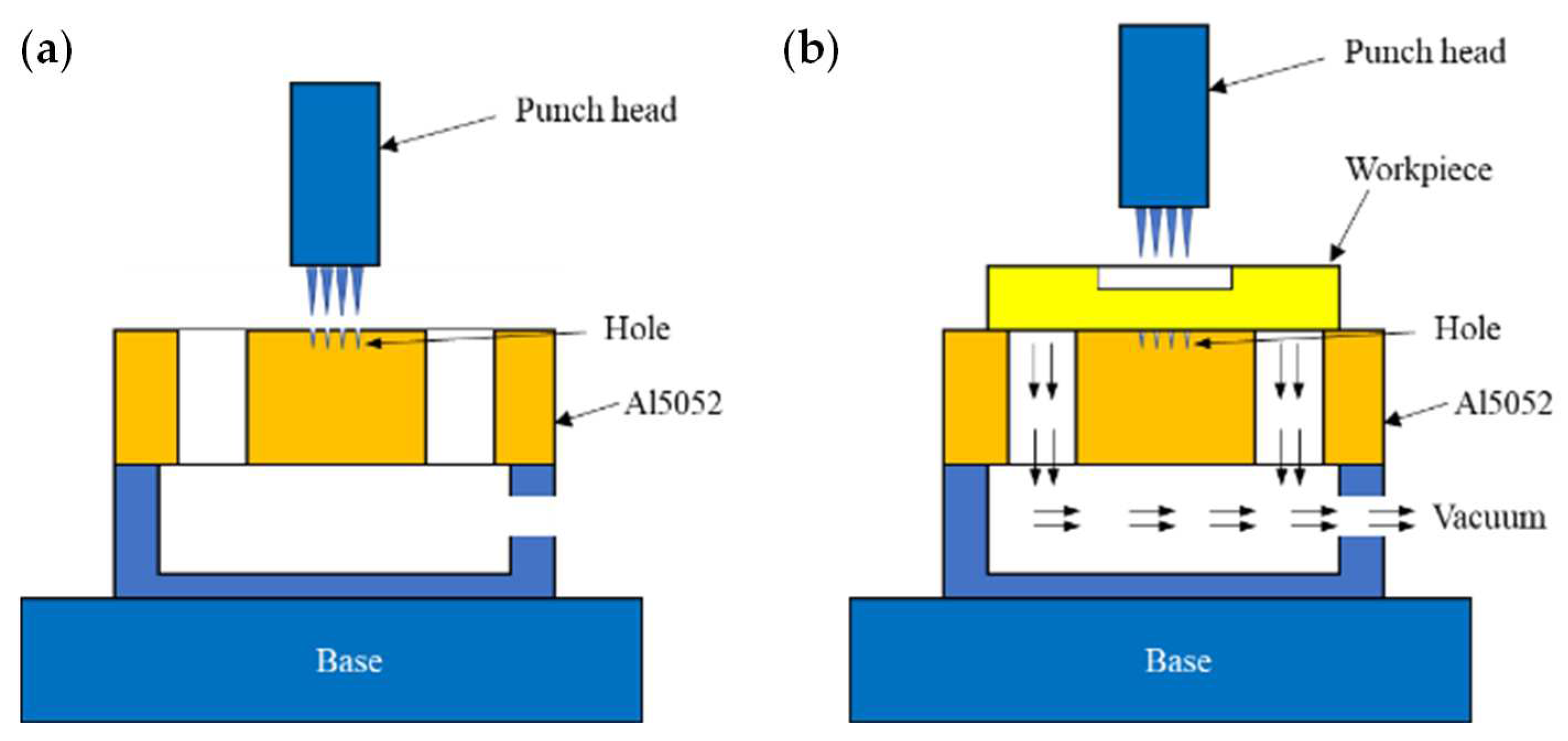
Figure 1. Stamping design (a) stamping lower die holes (b) stamping.
Preprints 71281 g001
Figure 2. Experimental equipment (Sodick AP1L) (a) stamping equipment (b) sample (c) punch head.
Preprints 71281 g002
Figure 3. Punch head manufacturing (a) electrode drilling (b) Reverse-EDM.
Preprints 71281 g003
Figure 4. Array punch head profile.
Preprints 71281 g004
Figure 5. Punch head appearance measurement.
Preprints 71281 g005
Figure 6. Design of stamping experiment.
Preprints 71281 g006
Figure 7. Array micro-holes (a) general view of inlet through OM (b) general view of outlet through OM (c) SEM inlet (d) SEM outlet.
Preprints 71281 g007
Figure 8.  Sample section.
Preprints 71281 g008
Figure 9. Residual material of punch head (a) front end of punch head (b) middle of punch head (c) selective enlargement (d) EDS before stamping (e) EDS after stamping.
Preprints 71281 g009
Figure 10. Microholes after grinding (a) general view of inlets (b) magnified inlet (c) general view of outlets (d) magnified outlet.
Preprints 71281 g010
Figure 11. Dimensions of microholes before and after grinding (a) inlet (b) outlet.
Preprints 71281 g011
Table 1. EDM parameters.
Experiment Circuit Current Discharge time Off time Shaking radius (R)
GM 0.1A 6μs 24μs 70μm
SF 1000pF 0 0 70μm
SF 1000pF 0 0 80μm
Disclaimer/Publisher’s Note: The statements, opinions and data contained in all publications are solely those of the individual author(s) and contributor(s) and not of MDPI and/or the editor(s). MDPI and/or the editor(s) disclaim responsibility for any injury to people or property resulting from any ideas, methods, instructions or products referred to in the content.
Copyright: This open access article is published under a Creative Commons CC BY 4.0 license, which permit the free download, distribution, and reuse, provided that the author and preprint are cited in any reuse.
Prerpints.org logo

Preprints.org is a free preprint server supported by MDPI in Basel, Switzerland.

Subscribe

© 2024 MDPI (Basel, Switzerland) unless otherwise stated