1. Introduction
The development of highly integrated microelectronic devices requires ever more efficient thermal management solutions. Efficient cooling systems are also very important to reduce the environmental impact of high-power density electronics cooling [
1]. Microfluidic heat sinks have proven to be an excellent solution to meet this challenge [
2]. Indeed, the high surface-to-volume ratio in microfluidic channels allows to achieve a very large thermal contact between the refrigerant and the heat exchanger. The cooling efficiency is further improved by the small thickness of the channel walls, which reduces the thermal resistance between the heat source and the refrigerant. Since this technology was first introduced in the 1980s [
3], numerous developments and optimizations were made [
4]. One of the most notable ones was the implementation of flow boiling in microchannels [
5], which allowed to reach even higher cooling power by using the refrigerant latent heat and to ensure a uniform temperature across the system.
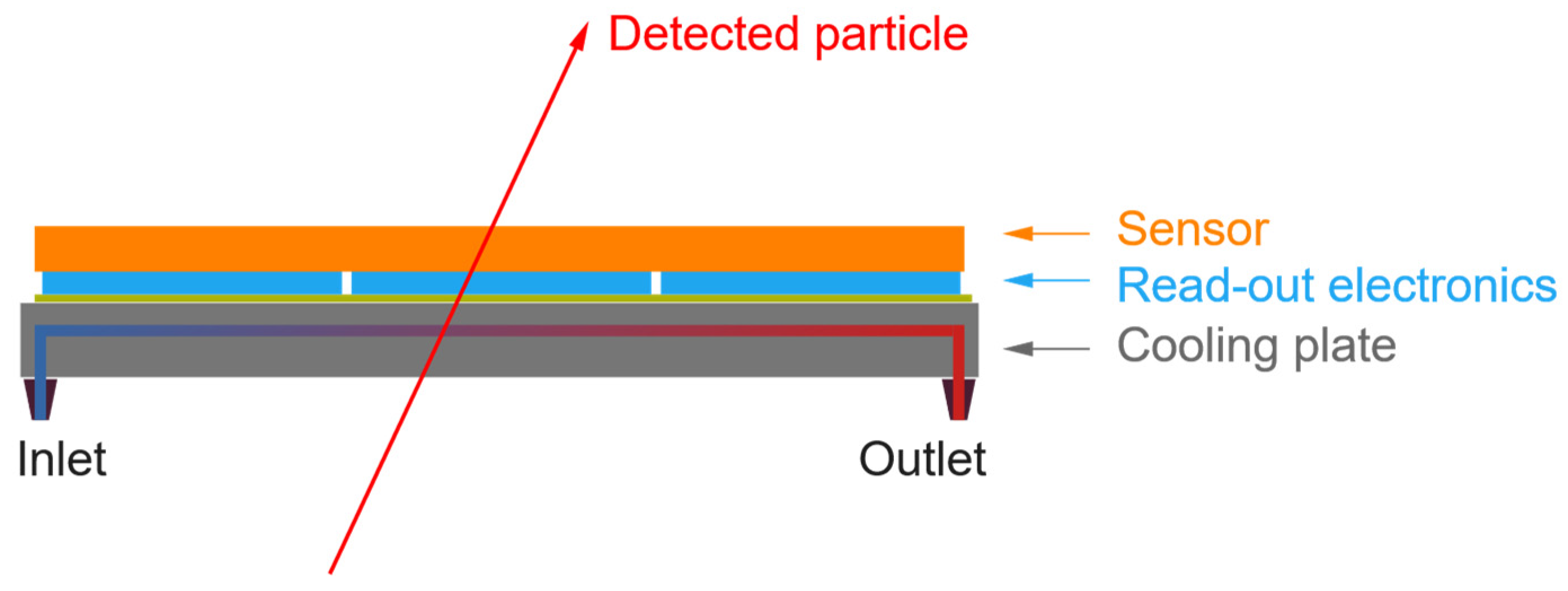
Since these seminal works, the microchannel cooling technology has found numerous applications in electronic systems featuring very demanding requirements. This article focuses on the application of this technology to the cooling of silicon pixel detectors used in particle physics experiments. A schematic diagram representing the typical layout of these detectors is presented in Figure 1. A silicon sensor, typically 100-300 µm thick, is connected to pixelated read-out electronic chips of about the same thickness. The resulting hybrid module has a typical size of a few cm2 and is glued onto a plate of matching size serving both as heat sink and mechanical support.
Figure 1.
Schematic diagram showing the typical layout of a silicon pixel detector used to detect the crossing of an impinging particle.
Figure 1.
Schematic diagram showing the typical layout of a silicon pixel detector used to detect the crossing of an impinging particle.
Although the power dissipation in these detectors remains moderate (1-3 W/cm²), the mechanical requirements on such systems are very stringent:
The sensor being operated at low temperature (typically -10 to -30°C) to mitigate the radiation damage, the coefficient of thermal expansion (CTE) of the cooling system must match that of the sensor;
As matter perturbs the trajectory of the impinging particles, the cooling plate should be made of a light material and remain as thin as possible (≪ 1 mm), while keeping the mechanical stability good enough to hold the detector;
When a boiling flow is used as a refrigerant, the cooling plate should be able to withstand a very high pressure (up to several hundred bars).
To fulfil these requirements, the particle physics community has developed silicon microchannels cooling plates. As of today, such devices have been implemented in two detectors, the NA62 GigaTracKer [
6] and the upgraded LHCb-VELO [
7]. Their specifications are reported in
Table 1. The pressure requirements for the LHCb-VELO upgraded detector have become particularly demanding with the use of bi-phase CO
2 as a refrigerant. Although the cooling system is at ~14 bar during normal operation at -30°C, at room temperature (20°C) the pressure reaches ~57 bar. For safety reasons, the entire system has been validated at 186 bar to prevent damages in case of sudden loss of cooling. Moreover, the future high-energy physics applications will face higher radiation dose and will probably need to operate at even lower temperature. Alternative refrigerants are envisaged such as bi-phase krypton [
8], which reaches ~100 bar at room temperature. For both the NA62 and LHCb detectors, the cooling plates were fabricated on 8-inch etched silicon-on-insulator (SOI) wafers, bonded together using either hydrophilic or hydrophobic direct bonding (DB) [
6,
7]. This fabrication process was reported to be challenging and expensive [
7]. The most critical steps were found to be the bonding of large and deeply etched SOI wafers and the soldering of the connectors. Despite these difficulties, the Si microchannel cooling offers unmatched performances that make it essential to build the detectors required for the next generation of particle physics experiments.
Table 1.
Specification of the cooling system of the two particle physics detectors implementing Si microchannels cooling [
6,
7].
Table 1.
Specification of the cooling system of the two particle physics detectors implementing Si microchannels cooling [
6,
7].
| Detector name |
Dimensions (cm²) |
Total Plate Thickness
(µm) |
Refrigerant Type |
Operating Pressure (bar) |
Operating Temp. (°C) |
| NA62 GigaTracKer |
7 × 8 |
210 |
Liquid C6F14
|
3 |
[-10;20] |
| Upgraded LHCb-VELO |
11.37 × 11.65 |
500 |
Bi-phase CO2
|
14-57 |
[-30;20] |
This work aims at improving the fabrication process of the microchannel cooling plates in terms of complexity and costs. As an alternative to Si-Si direct bonding (DB), we propose two wafer bonding techniques:
These two techniques are widespread and have, in principle, less stringent requirements in terms of surface quality and process control, which may translate into higher production yields of the cooling plates. A further reduction of the fabrication cost is expected by using standard Si wafers instead of SOI wafers as well as by decreasing the bonding temperature, which may typically reach 400-700°C for hydrophobic or 800-1100° for hydrophilic Si-Si DB [
9]. Although intermediate layers are involved (glass for AB and gold for TC), they are chemically stable and compatible with the refrigerant fluids in the microchannel. Furthermore, the small thickness of these intermediate layers makes the material added to the silicon substrate negligible.
Anodic bonding with thin-film sodium-borosilicate glass, introduced in 1972 for pressure sensors [
10], has proven to be an interesting bonding method for microsystem technology. It offers similar bonding performance as standard AB with bulk glass (typ. 0.5 - 1 mm thick) but with much higher compactness. Due to the small thickness of the deposited glass (typ. 2 - 10 µm), AB of Si-Glass-Si can be performed at significantly lower bonding voltage (typ. 50-200 V) and temperature (300-350
oC), introducing lower stress into the bonded system. Nevertheless, the deposition process of glass must be optimized to ensure its appropriate composition, thermal and dielectric properties (high electrical breakdown voltage) as well as acceptable surface roughness and residual stress. Si-Glass-Si anodic bonding with 2 µm Pyrex 7740 glass (Corning), sputtered on 0.3 µm SiO
2, was investigated by Hanneborg et al. for sensor applications, demonstrating strong bond at 400
oC and 200 V, applied during 10 min [
11]. When compared to sputtering, the e-beam evaporation method, especially plasma-assisted, allows to deposit glass layers with lower surface roughness (nm range) and lower residual stress, providing also the compatibility with lift-off process [
12]. Sassen et al. fabricated a hermetically sealed Si-Glass-Si resonator, bonded at 450-500
oC and 100 V, using an e-beam evaporated 1.5 µm layer (Ra~5 nm) of Schott #8329 glass [
13]. Conti et al. demonstrated a Si-Glass-Si microfluidic flow control valve, bonded at 350
oC and 200 V with plasma-assisted evaporated 10 µm Schott Borofloat33 (BF33) glass layer, allowing infusion of viscous fluids at high operating pressure up to 20 bar [
14].
TC bonding is considered as a versatile, low cost, and industrially attractive method that can be achieved with a wide variety of thin-film metal layers and using different deposition methods, mainly magnetron sputtering, e-beam evaporation and electrodeposition. Among various TC systems, bonding with gold (Au-Au) is the most popular solution due to easy plastic deformation of gold and its high chemical stability (oxidation resistant), leading to less demanding process requirements. Since Au creates a eutectic system with Si at ≥ 363
oC, the gold TC bonding on Si substrates is typically carried out at a lower temperature (250-350
oC) and may involve additional barrier layers (NiCr, TiW, Pt) to prevent the thermodiffusion of gold. Tsau et al. achieved a strong bond between e-beam evaporated Ti/Au (100/800 nm) layers, applying 0.5 MPa pressure for 10 min at 300
oC [
15]. Goorsky et al. reported that hermetic Au-Au bonds can be realized at 200°C under 3 MPa pressure during 15 min, using sputter deposited TiW/Au (400/1200 nm) films with intermediate values of initial surface roughness (3-5 nm) [
16]. Hermetic Au-Au bonding for wafer-level MEMS packaging was also reported by Charlot et al. [
17]. TC process was carried out at 420
oC and 5.7 MPa using electroplated 3000 nm Au on evaporated TiW (50 nm) diffusion barrier and Ti/Au (50/500 nm) seed layers.
In this work, we report a comparison of the pressure resistance of microfluidic test structures, fabricated by AB and TC bonding methods. The main goal is to verify the compatibility of these bonding methods with microcooling applications where a very high-pressure resistance (≥ 200 bar) is required. The bonding was performed on 4-inch Si wafers, using evaporated BF33 glass (AB) and sputtered Ti/Au (TC) as intermediate layers. This TC metal configuration was selected to be simple and easily accessible. The two tested bonding methods are found to offer sufficient bond quality to hold the high pressure required for the particle physics detectors application. In addition, these bonding techniques can potentially also be used to bond connectors to the cooling plates.
2. Materials and Methods
The bonding strength was evaluated indirectly as in [
7], performing a destructive pressure burst test. The maximum internal pressure reached in a microfluidic test structure was measured before breakage. The chips fabrication starts with the etching of a series of structures on a silicon 4-inch diameter wafer. The etched wafer is then bonded to a second silicon wafer in order to close the microfluidic structures. Finally, the wafer is diced into chips, containing each a single structure, which is then pressure burst tested. The implemented chip fabrication processes and the pressure test setup are described in this section.
2.1. Design of test structures
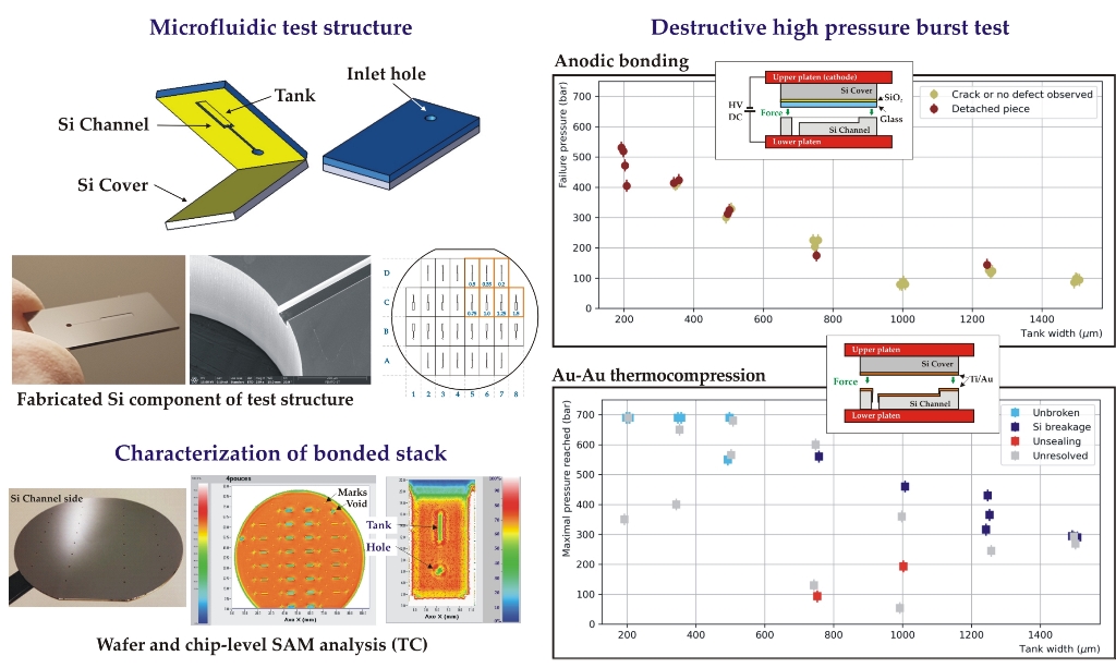
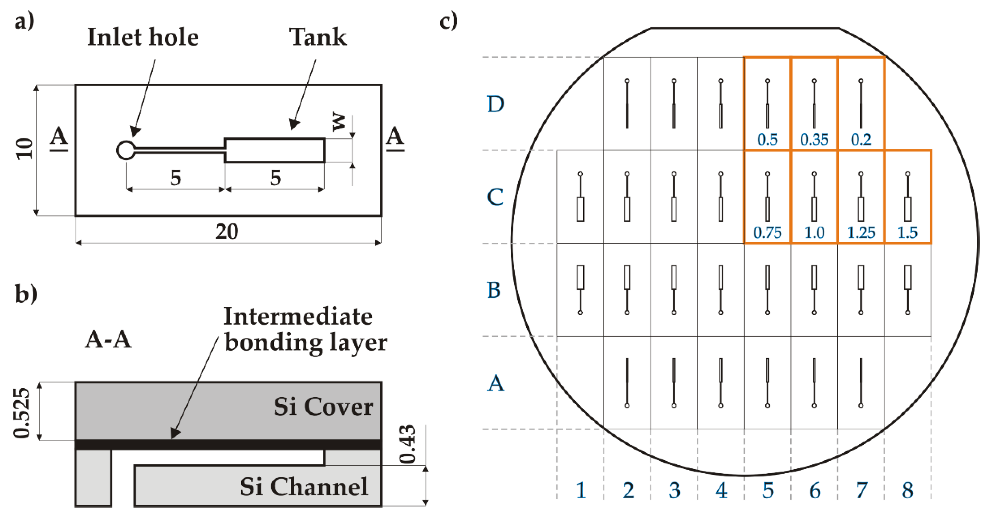
The microfluidic test structure (20×10 mm2) consists of a top flat cover part bonded to a micromachined channel part, using an intermediate bonding layer (glass or gold depending of the bonding method), as shown in Figure 2. The channel part contains a single rectangular tank that is fed by an inlet hole (0.8 mm diameter) through a narrow straight channel (50 µm wide). The tank and the channel are 5 mm long and 70 µm deep. Both the channel and the cover parts are 525 µm thick, such that the minimal wall thickness of the tank is ~455 µm. At the wafer level, 28 test structures were designed with seven different types of structures with variable tank widths (w=0.2/0.35/0.5/0.75/1.0/1.25/1.5 mm), as presented in Figure 2. The total bonding surface is 76.6 cm2.
Figure 2.
Design of the test structures: a) top view of the channel part; b) side view of an individual chip after bonding; c) wafer-level design of the channel structures with tank widths (in mm) chip naming convention (top-right quarter is mirrored along X and Y axes).
Figure 2.
Design of the test structures: a) top view of the channel part; b) side view of an individual chip after bonding; c) wafer-level design of the channel structures with tank widths (in mm) chip naming convention (top-right quarter is mirrored along X and Y axes).
2.2. Fabrication and characterization of test wafers
2.2.1. Cover wafer for AB
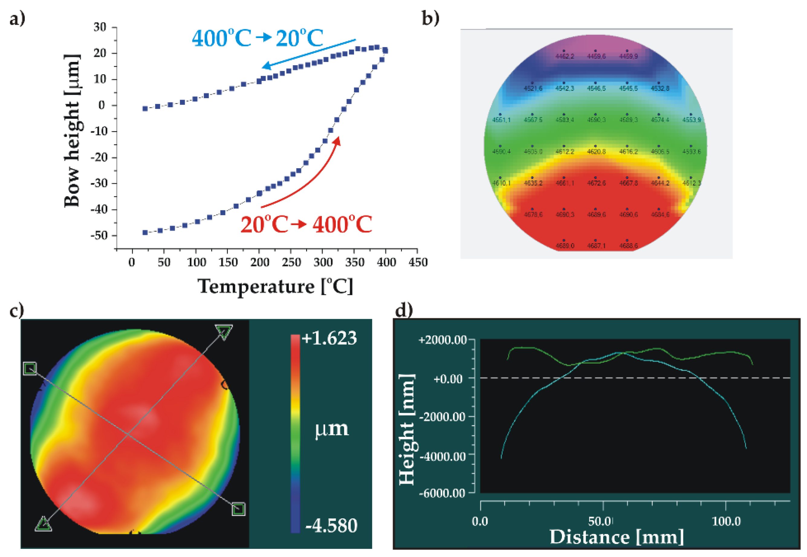
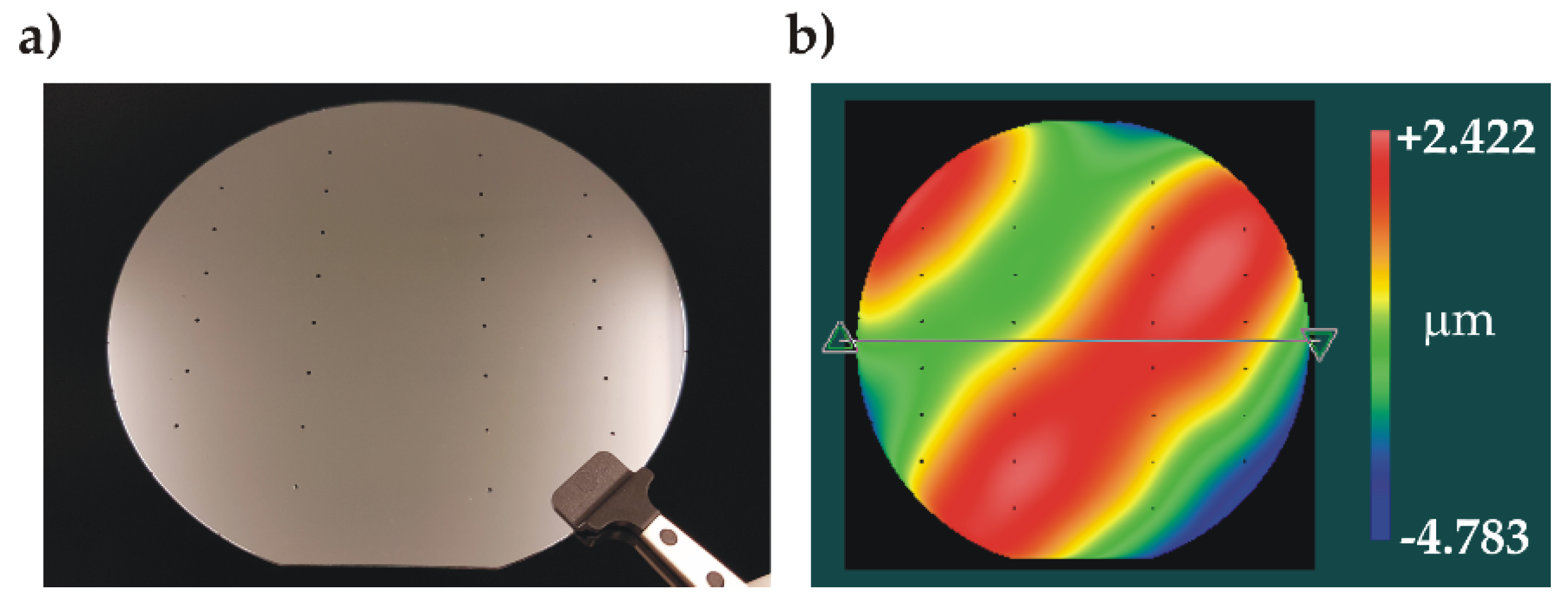
The cover wafer used for the AB process is a 4-inch diameter 525 µm thick silicon wafer (p-type) with a SiO2/BF33 glass layer deposited on one side. The 4 µm thick BF33 layer was deposited by plasma-assisted evaporation method on a Si wafer coated with 1 µm SiO2. The coated wafer was purchased as such from MSG Lithoglas GmbH (Dresden, Germany) and was characterized in terms of 3D surface profile (ZYGO Verifire GPI XP interferometer) and glass surface roughness (Bruker Dektak XTA profilometer). The glass layer uniformity was measured with an optical reflectometer (F50-EXR, Filmetrix Inc, US) in the wavelength range of 380-1700 nm. The wafer curvature was also measured as a function of temperature with a thin-film stress measurement system (FSM500TC) to verify if the initial residual stress of the deposited thin-films could be released by annealing before or during bonding process. The temperature was changed in two steps: heating from 20oC to 400oC (5oC/min) and cooling phase from 400oC to 20oC (natural) while measuring the wafer profile evolution.
2.2.2. Cover wafer for TC bonding
The cover part is a double side polished (DSP) 525 µm thick, 4-inch and n-type (100) wafer with a total thickness variation (TTV) less than 1 µm. This low TTV is chosen to fulfil the more stringent requirements of TC bonding when compared to anodic bonding. The cover wafer was selected among a few candidates so that its 3D surface profile matches the channel one.
2.2.3. Channel wafers
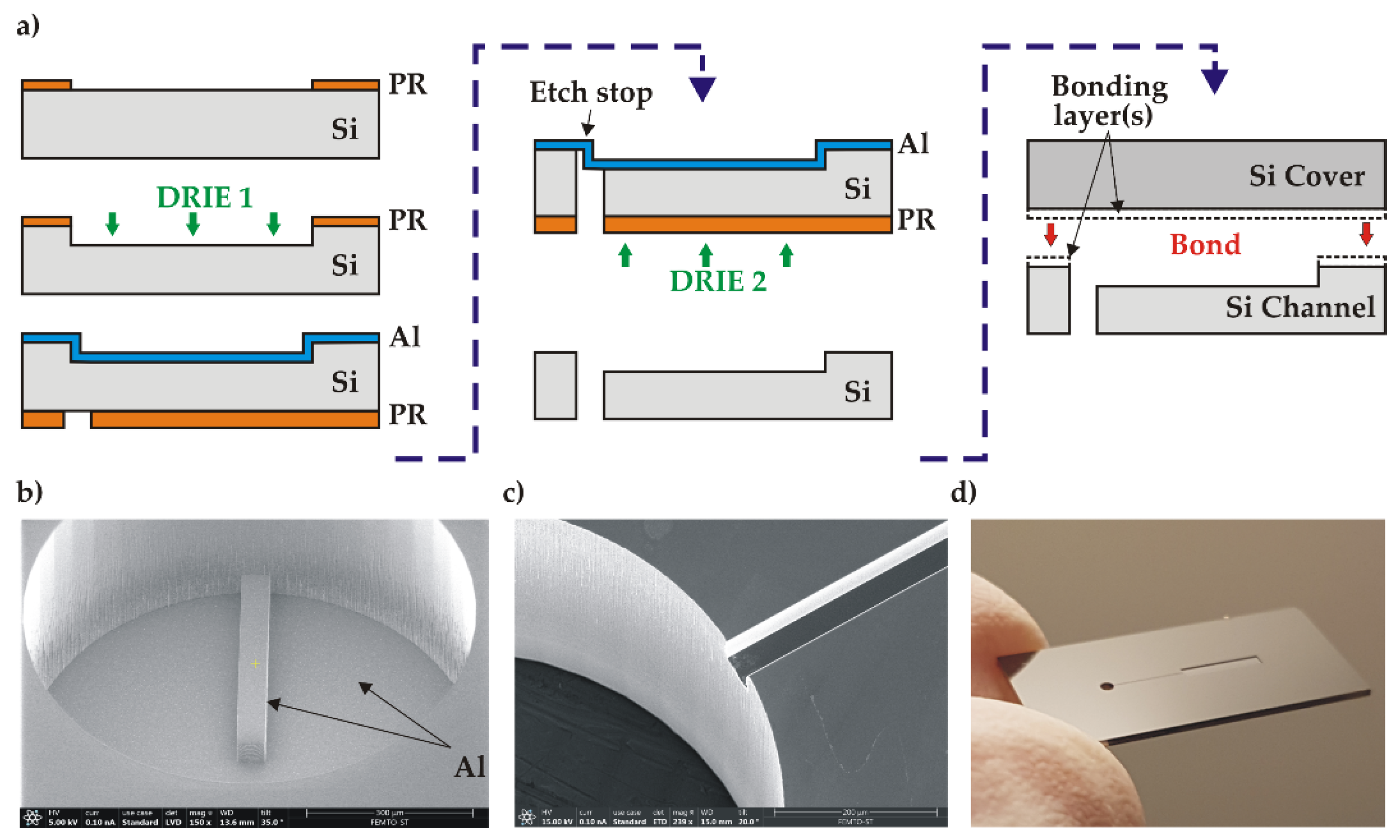
The channel wafers were prepared on 525 µm thick, 4-inch and n-type (100), DSP silicon substrates with resistivity of 1-10 Ω.cm and TTV<3 µm. Two successive DRIE etching processes were performed using a SPTS Rapier system, as shown in Figure 3a. For the first etching of channels (DRIE1), a 1.2 µm thick layer of S1813 photoresist (PR) was spin-coated on the wafer front side with a Suss Microtec ACS200 coater and photolithographically patterned using an EVG601 aligner. The channels were then etched to a depth of (70 ± 2.5) µm. For the second etching of inlet holes (DRIE2), a 0.6 µm thick aluminium layer was first magnetron sputtered (Plassys MP700) on the already etched wafer front side in order to create an etch stop layer. Next, a 6 µm thick AZ10XT photoresist (Microchemicals) was spin-coated and patterned on the wafer back side, followed by the DRIE etching through the wafer until exposing the Al etch stop (Figure 3b). The average etch rate was 10 µm/min and the Si etch selectivity over PR 150:1. After the DRIE etching, the photoresist mask was stripped in acetone and the wafer underwent a O2 plasma cleaning using a Tepla Gigabatch 360. As a last step, the aluminium layer was removed in a commercial Al etch solution at 40oC. The channel depth as well as the depth uniformity across the wafer were measured using a DEKTAK profilometer and SEM inspection. The homogeneity of the etching depth (target 70 µm) was (70.3 ± 0.2) µm. The obtained channel structure is presented in Figure 3c, d.
Figure 3.
Fabrication of the test structure: a) simplified flow-chart; b) SEM image of the inlet hole etching (DRIE 2) with the exposed Al stop layer; c) SEM image of inlet hole and channel after Al removing; d) Si channel part after wafer dicing.
Figure 3.
Fabrication of the test structure: a) simplified flow-chart; b) SEM image of the inlet hole etching (DRIE 2) with the exposed Al stop layer; c) SEM image of inlet hole and channel after Al removing; d) Si channel part after wafer dicing.
2.3. Bonding procedure
2.3.1. Wafer preparation
Before bonding, the wafers were cleaned in acetone and ethanol to remove dust and basic organic contaminants. The cover wafers (both for AB and TC) were wet cleaned in a Piranha solution (H2O2:H2SO4, 1:2) and rinsed in deionised (DI) water. Due to the deep structuration of the channel wafers and the potential problems when rinsing away the viscous Piranha solution in DI water, they were dry cleaned by O2 plasma in the Tepla GIGABatch360M microwave reactor (parameters 300 W, pressure 0.8 mbar, O2 flow 50 sccm). The cleaned wafer pairs were either used directly for AB or underwent the Ti/Au thin-film deposition procedure for TC bonding.
2.3.2. Bonding equipment
All bonding processes were performed in an AWB04 bonder (AML Ltd, United Kingdom), which allows the integration into a standard bonding recipe of several in-situ operations, such as optical alignments, surface O2 plasma treatments or DI water vapour injections. In the AB configuration, graphite and tungsten platens were installed as upper (cathode) and lower (anode) platens, respectively. A specific wafer side-clamping on the upper platen allowed to avoid any contact between the bonding surfaces and the bonder parts (flags, jigs, etc.). The wafer alignment was made either at room temperature (TC) or at bonding temperature (AB).
2.3.3. Anodic bonding process
In order to achieve a stable bonding without electrical breakdown in the very thin glass layer, a voltage in the range of 30-60 V and a temperature around 300
oC are in principle sufficient [
12]. Nevertheless, in this work the voltage value has been increased to 180 V due to the thickness of the oxide layer (1 µm) in the bonding stack.
The process started by a surface activation using a radical activation system (RAD) with O2 plasma. It was carried out in the vacuum chamber of the bonder in the configuration presented in Figure 4a. The activation was performed over 10 min with RAD voltage and current set to 600 V and 100 mA, respectively. The activated surface was then treated in-situ by DI water vapours to complete the hydrophilization procedure. To relax the residual stress, the cover wafer underwent a short annealing in vacuum at 400oC during 20 min, while keeping the channel wafer at 150oC. Once the temperature of the two wafers was stabilized at the desired bonding temperature (350°C), they were aligned and contacted with a bonding force of 500 N. The AB process was carried out by applying the DC voltage progressively up to 180 V keeping the bonding current limited to 4 mA, as shown in Figure 4b. This method ensured the uniformity of the bonding current, reducing the stress level in the bonded stack. The bonding process was carried out for 15 min. The total transferred charge was measured around 750 mC.
Figure 4.
Anodic bonding: a) Schematic of the bonding setup; b) Voltage and current measured during the bonding process.
Figure 4.
Anodic bonding: a) Schematic of the bonding setup; b) Voltage and current measured during the bonding process.
2.3.4. Au-Au thermocompression bonding
The adhesion (Ti) and bonding (Au) layers were deposited immediately after the channel and cover wafers had been cleaned. The deposition was done by magnetron sputtering in an automatic MP700 machine (Plassys, France). The process started with the evacuation of the chamber to a background pressure of 10-5 Pa. The distance between the planar cathodes and the substrate was then set to 10 mm and the surfaces were prepared for the subsequent thin-film depositions with an Ar reactive plasma. Finally, the layers were deposited at a working pressure of 0.9 Pa: the 20 nm thick adhesion layer with a target current of 1 A first, followed by the 350 nm thick Au bonding layer with a target current of 0.3 A. A thickness non-uniformity of ±11% was obtained with a tensile stress of 110 MPa. The average roughness (Ra) of Au surface was 1.09 nm.
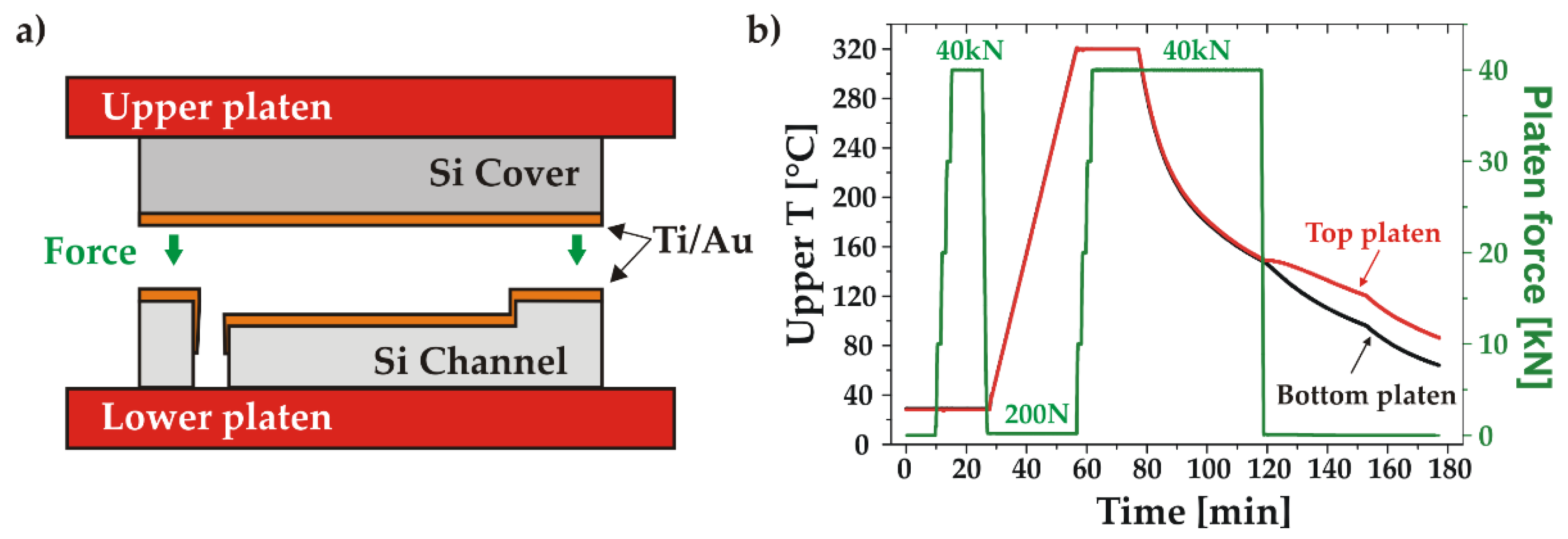
After the Ti and Au depositions, the wafers pair was installed in the bonder and the chamber was evacuated to 7.0×10⁻⁵ mbar. After alignment, a pre-bonding step was performed at room temperature under a piston force of 40 kN (5.22 MPa) during 5 min. Next, the wafers temperature was ramped up while keeping a small controlled force of 200 N, followed by a final bonding step at a temperature of 320°C and under a force of 40 kN during 20 min. The bonded stack was held under pressure during controlled cooling down to 150°C. The registered temperature and force characteristics of the bonding process are shown in Figure 5.
Figure 5.
Thermocompression Au-Au bonding: a) schematic of the bonding setup; b) measured temperature of the upper (red) and lower (black) platens and applied force (green) during the bonding process.
Figure 5.
Thermocompression Au-Au bonding: a) schematic of the bonding setup; b) measured temperature of the upper (red) and lower (black) platens and applied force (green) during the bonding process.
2.4. Acoustic Imaging analysis
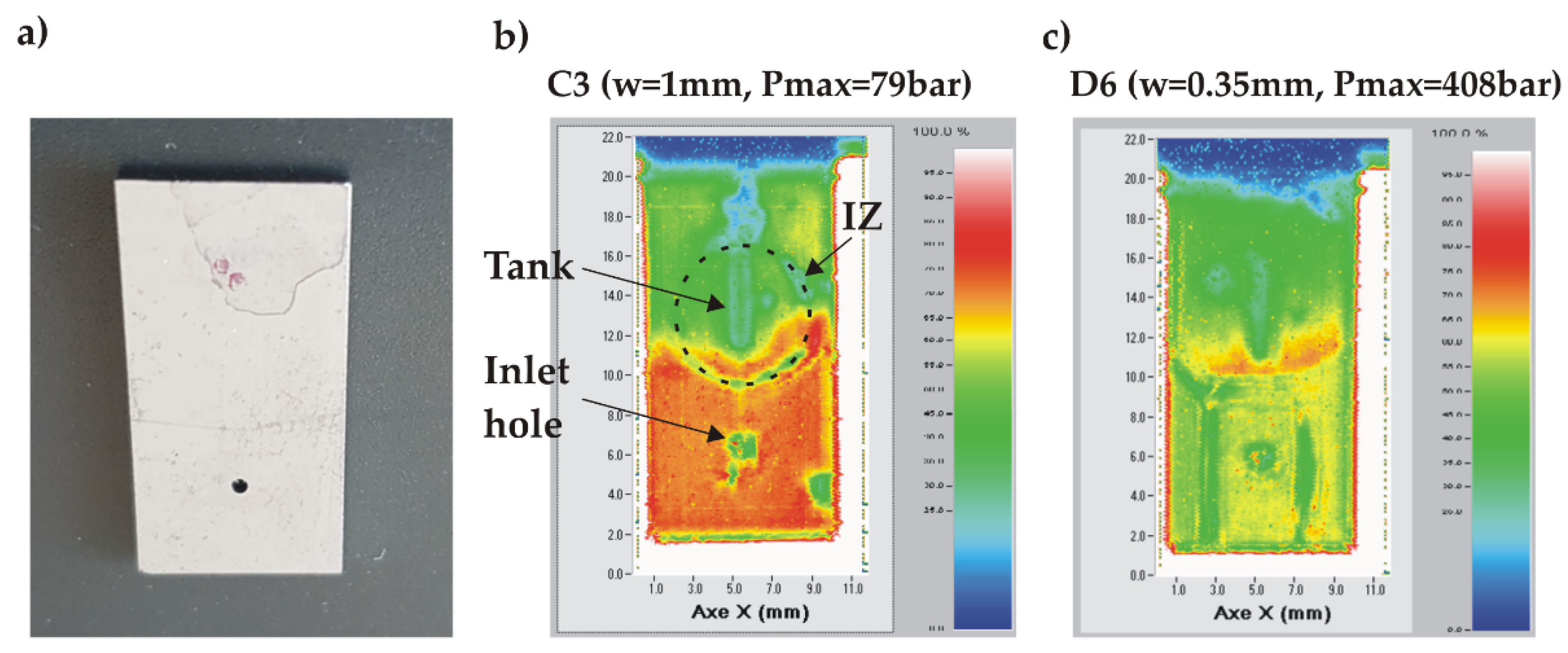
Scanning acoustic microscopy (SAM) in transmission mode was used to visualize possible defects at the Au-Au bonding interface in the wafers stack as well as in the individual test structures (after dicing). The employed home-made SAM system was equipped with two focalized acoustic transducers (Sonaxis, France) integrated on an X-Y-Z translation stage and with an emitter/receiver controller (Sofranel, France). The transducers have an active diameter of 19 mm, a focal length of 30 mm and operate at a central frequency of 15 MHz, providing an imaging resolution close to 200 µm (-6 dB). Figure 6 shows the water reservoir with the test sample clamped in the Teflon holder. In the calibration procedure, the attenuation was adjusted such that the highest impedance signal on the sample corresponded to 70% of the full scale. As a result, the area with the highest acoustic transmission in the tested sample (best bonding quality) is represented by red/orange in SAM images, whereas bonding defects (voids) or air-filled channels larger than 200 µm are clearly visible as green/blue areas.
Figure 6.
Scanning Acoustic Microscopy (SAM) measurements of Au-Au bonded wafers: a) home-made SAM system, zoom on water tank with emitter/receiver and sample holder; b) zoom on the sample holder, c) typical SAM image of well bonded test structure.
Figure 6.
Scanning Acoustic Microscopy (SAM) measurements of Au-Au bonded wafers: a) home-made SAM system, zoom on water tank with emitter/receiver and sample holder; b) zoom on the sample holder, c) typical SAM image of well bonded test structure.
2.5. Wafer dicing
A dicing process of the bonded wafer stacks was performed by use of automatic high precision dicing saw DAD321 from DISCO (Japan), operating with standard 100 µm wide dicing blade.
2.6. Pressure resistance test bench
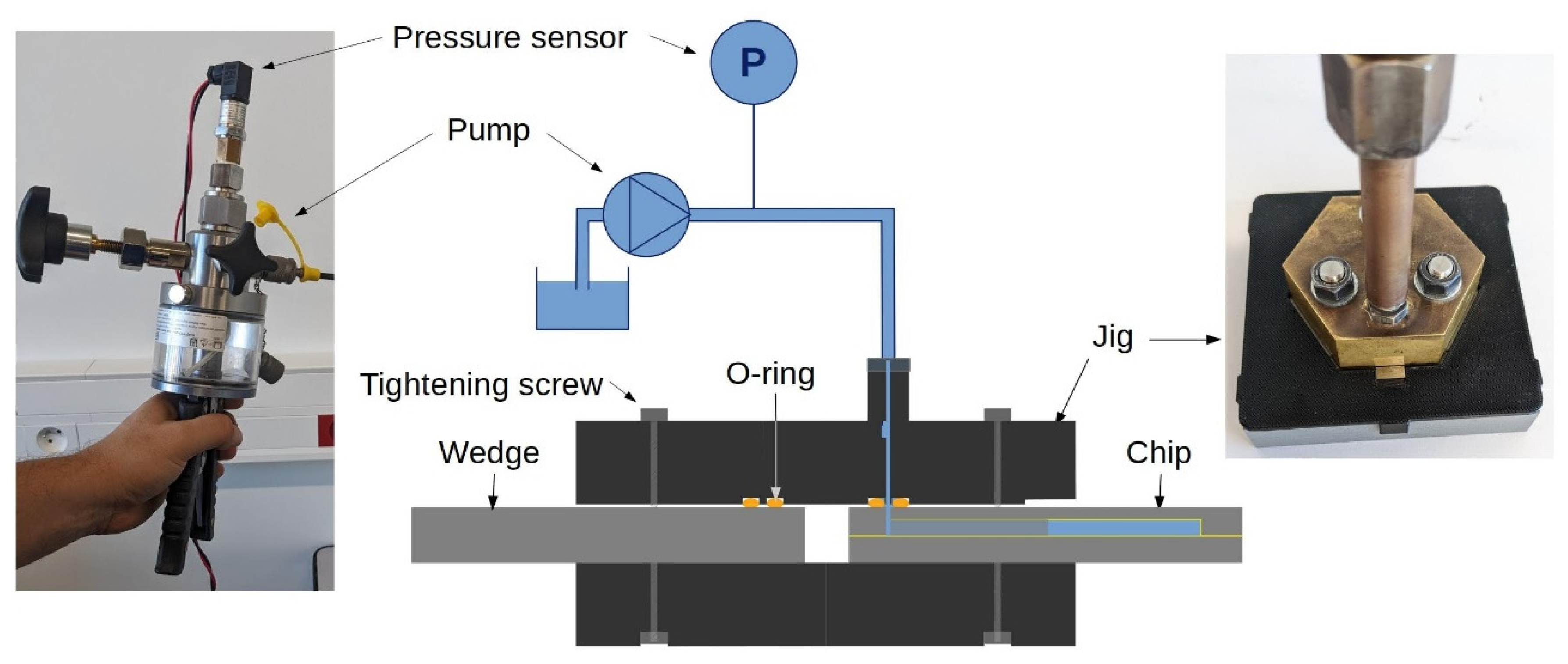
A dedicated test bench was set up to measure the pressure resistance of the bonded test structures (Figure 7). It consists of a hydraulic hand pump (Wika CPP700-H), which generates a pressure up to 700 bar through a handle or a fine adjustment vernier. The pump is filled with DI water and instrumented with a pressure sensor (Gems/3100). The sensor delivers a 4–20 mA analog signal proportional to pressures up to 700 bar, which is converted to a voltage in the range 0–5 V through a resistor. This analog signal is digitized with a 12-bit ADC (Microchip MCP3208, Chandler, AZ, United States) and converted to a 3.3 V level using a 4-channel level converter (Adafruit BSS138, New York City, NY, United States). The resulting signal is read-out on the SPI bus of a micro-computer with digital I/O capabilities (Raspberry Pi3 model B, Cambridge, United Kingdom). The measurements are recorded at a rate of ~3 Hz using a custom Python-based data acquisition software. A manufactured-in-house jig allows to connect the outlet of the pump and the inlet of the test structure. The sealing is ensured by an O-ring of 2 mm inner diameter and 1.6 mm cross-section embedded in a groove of 7 mm external diameter.
Figure 7.
Schematic of the high-pressure bench for destructive measurement of pressure resistance of test structures.
Figure 7.
Schematic of the high-pressure bench for destructive measurement of pressure resistance of test structures.
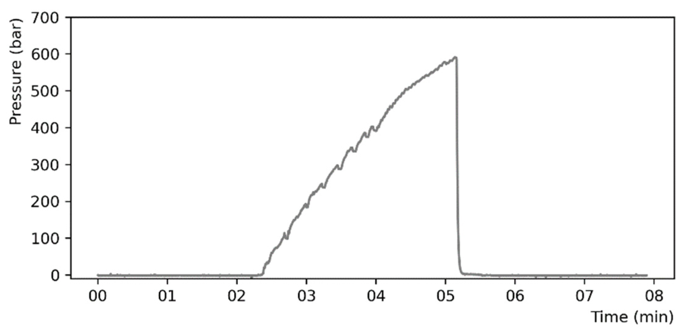
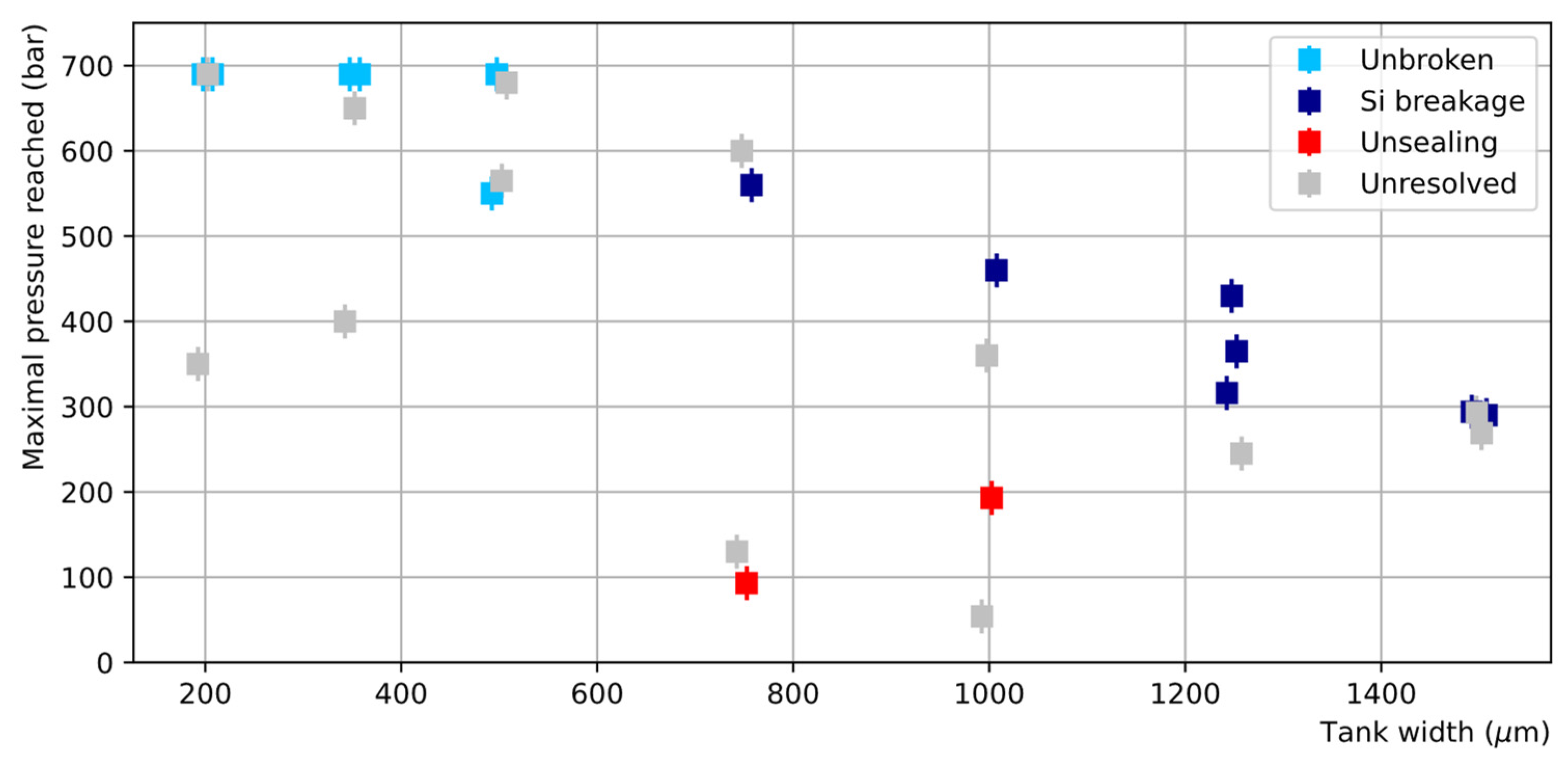
The test bench was used to perform destructive stress tests on the bonded chips. The pressure inside the microstructure was raised until the failure of the chip, identified as a sudden pressure drop, or until the maximum attainable pressure was reached (690 bar). The pressure characteristic, recorded during a typical measurement, is shown for illustration in Figure 8. The precision on the maximum pressure measurement has been estimated to be around ±20 bar.
Figure 8.
Typical rise of pressure inside a chip recorded with the high-pressure bench.
Figure 8.
Typical rise of pressure inside a chip recorded with the high-pressure bench.
2.7. Analysis after high-pressure destructive test
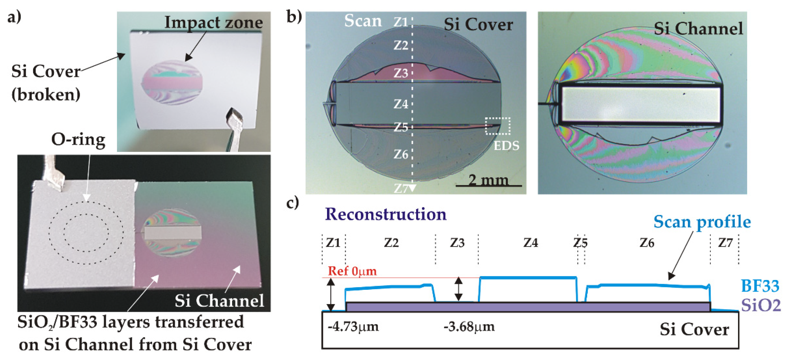
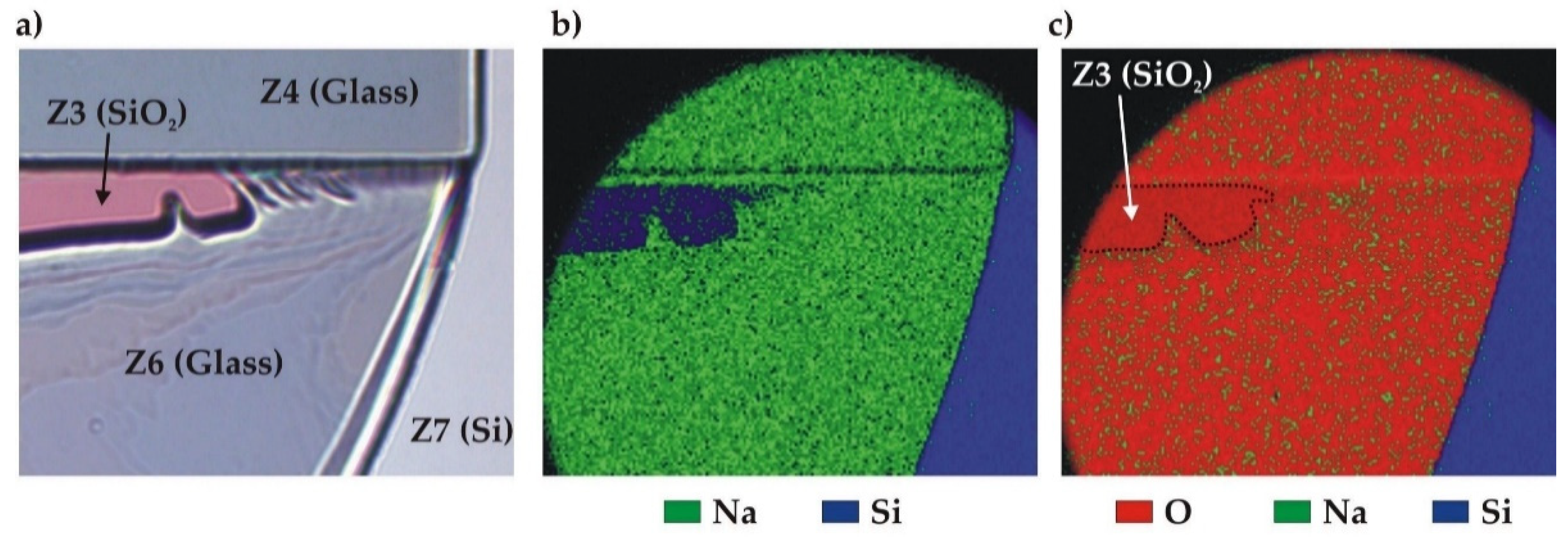
Broken samples with exposed bonding interface were investigated under optical microscope (Leica DM8000) to identify, when possible, the failure mode. Surface profile measurements were performed using mechanical profilometer after sample wet cleaning (Acetone/Ethanol/Piranha). The SAM imaging was also performed on samples that preserved their integrity after the burst pressure test.
4. Discussion
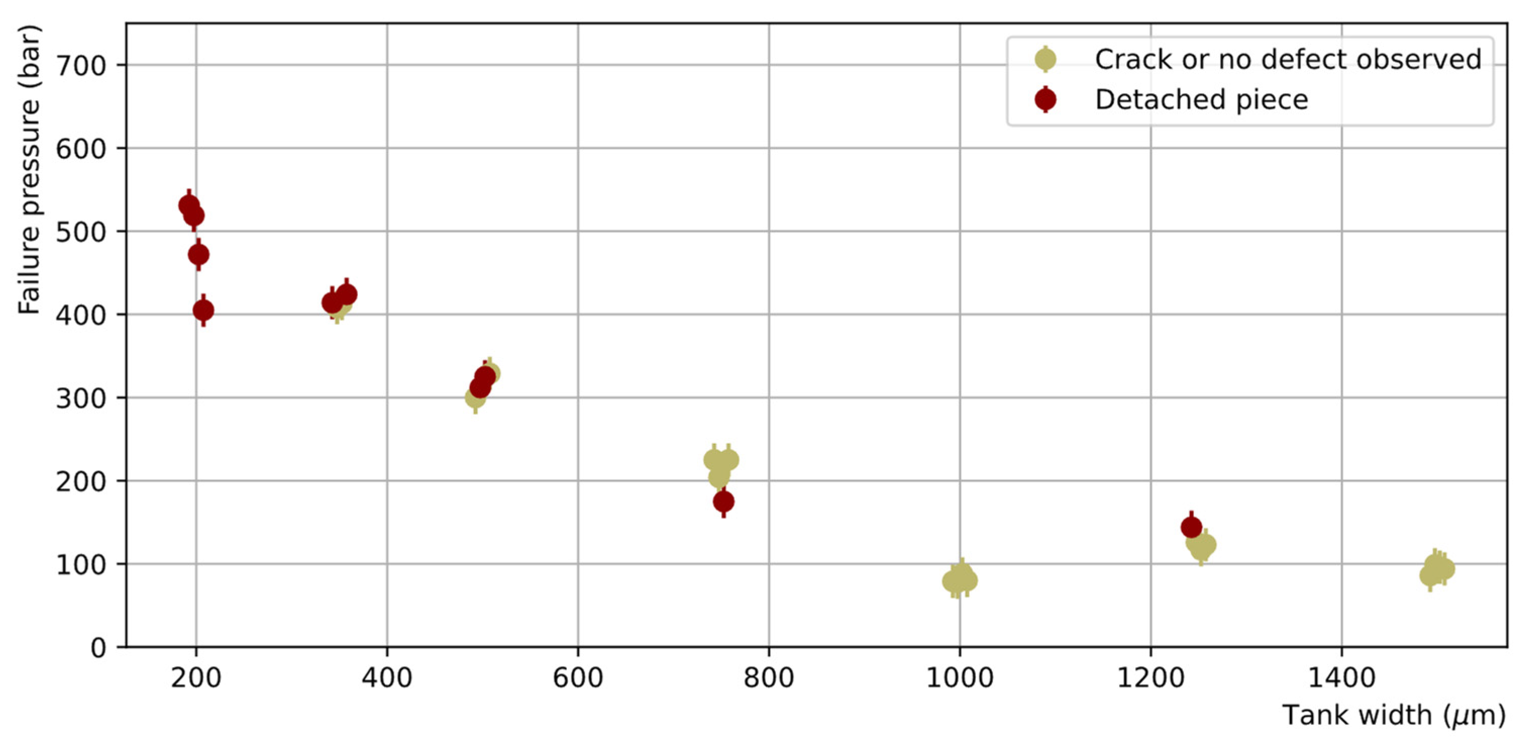
The obtained results show several advantages of the Si-Glass-Si AB, including a good pressure resistance (tested samples with w ≤ 500 µm sustained at least 250 bar) and a very good reproducibility of the failure pressures. Moreover, the AB process generates little stress in the bonded wafer stack. However, even if AB may be performed with standard bonding equipment, the access to this technique is limited. The plasma-assisted evaporation of a BF33 layer is not a common method in cleanroom facilities.
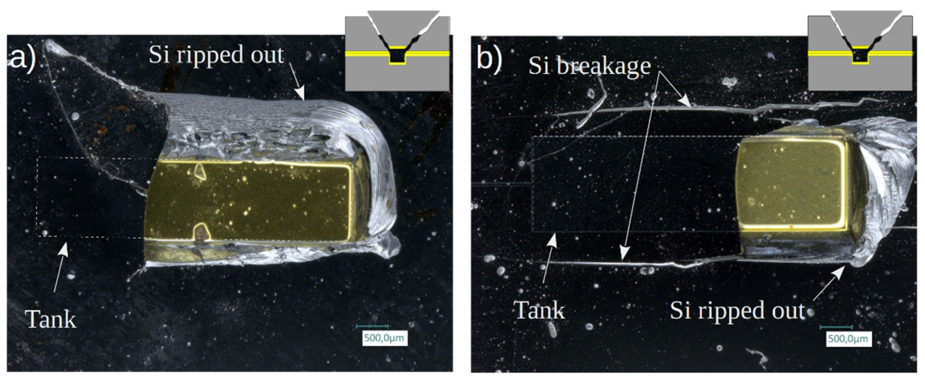
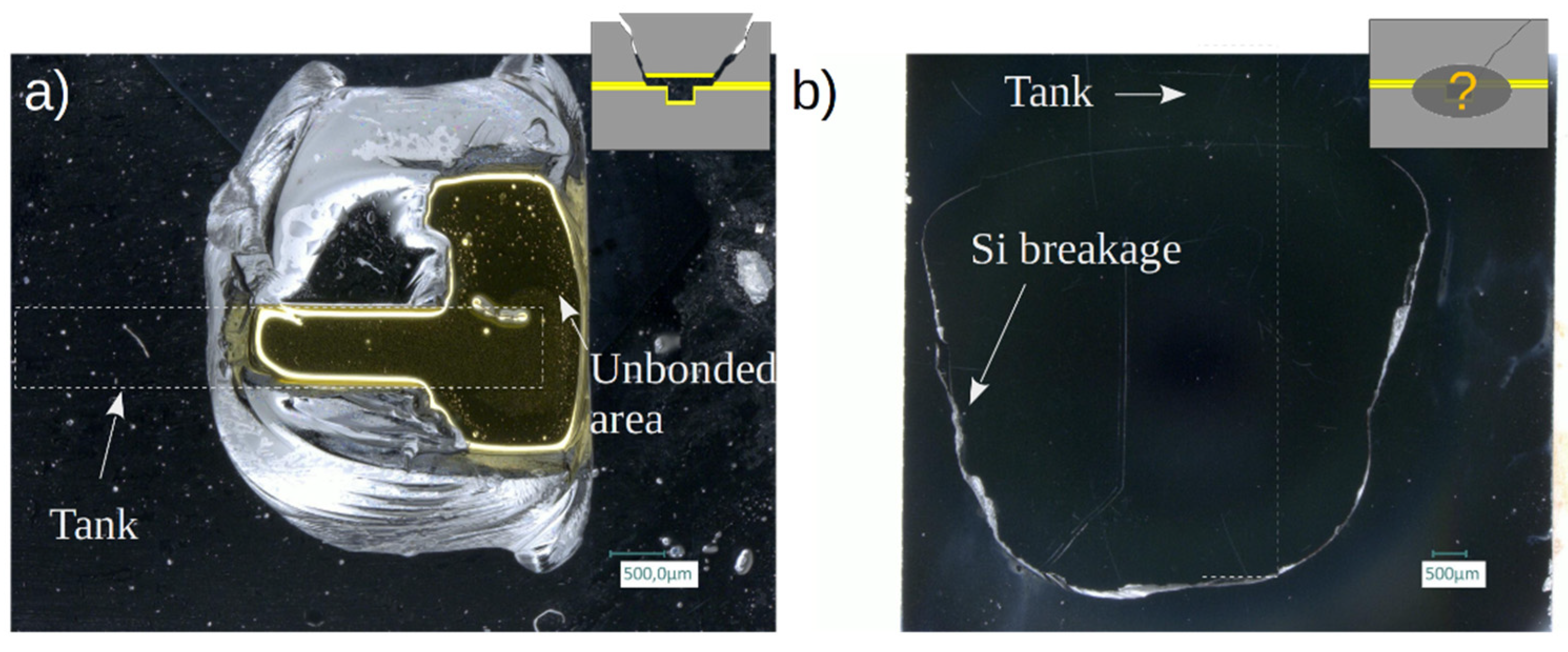
The TC bonding can also be considered as a very appealing technique as it is widespread and available in most cleanroom facilities. The maximal pressure values reached by the TC samples generally surpass these of the AB ones, the limitation in the TC case being generally set by the Si strength. As the TC is also a simpler process in terms of substrate preparation and process control than the AB, it appears to be a more promising technology. However, the reproducibility of the results is not as good as for the AB. Two components account for this variability. On one hand, the presence of a few outliers breaking at unexpectedly low pressures, and, on the other hand, the intrinsic dispersion due to the breaking mechanism in Si. In contrast, the delamination of the deposited layers in the AB samples seems to occur at a critical pressure value, leading to a lower dispersion of the failure pressures. The TC outliers, such as the one shown in
Figure 19a, are probably due to local defects on the bonding interface such as a hard particle or other local variations affecting the bonding quality. From this perspective, further optimizations of the presented TC process are necessary. Several optimization actions can be undertaken including the reduction of the particle contamination, the improvement of the metal thickness uniformity (currently ±11%) and the improvement of the bonding pressure uniformity. Moreover, the bonding strength may be affected by the thermal interdiffusion between the deposited metal layers and Si substrate at 320
oC, which could be avoided by use of an additional diffusion barrier layer.
A comparison of the maximum failure pressures reached with the AB and TC methods reported in this work and the ones obtained with DB in [
7] is presented in
Table 3. Although the Si thickness is smaller in the DB case, making direct comparison with this work difficult, this comparison suggests that the TC bonding could be as good as the DB. Indeed, the maximum failure pressure is limited by the Si strength in both cases.
Table 3.
Comparison of the maximum failure pressures reached in various conditions.
Table 3.
Comparison of the maximum failure pressures reached in various conditions.
| Bonding type |
Tank width |
Min. Si thickness |
Max. failure pressure |
Failure type |
Ref. |
| DB |
200 µm |
140 µm |
>450 bar |
No failure |
[7] |
| AB |
200 µm |
430 µm |
530 bar |
Interface |
This work |
| TC |
200 µm |
430 µm |
>690 bar |
No failure |
This work |
| DB |
500 µm |
140 µm |
280 bar |
Si breakage |
[7] |
| AB |
500 µm |
430 µm |
330 bar |
Interface |
This work |
| TC |
500 µm |
430 µm |
>690 bar |
No failure |
This work |
| DB |
1250 µm |
140 µm |
80 bar |
Si breakage |
[7] |
| AB |
1250 µm |
430 µm |
125 bar |
Interface |
This work |
| TC |
1250 µm |
430 µm |
430 bar |
Si breakage |
This work |
Author Contributions
Conceptualization, S.B., S.Be., J.C., M.P.-T.; Methodology, S.B (bonding, characterization), S.Be., J.C., M.P.-T. (pressure tests), S.Q. (dry etching), M.R. (EDS analysis), L.G-M (dicing), S.O. (thin-film deposition); Software, J.C.(pressure test); Formal analysis, S.B., J.C, M.P.-T.; Investigation, S.B., S.Be., J.C., M.P.-T., S.Q.; Resources, S.Be., O.L.; Data curation, S.B., S.Be., J.C., M.P.-T., S.Q.; Writing—original draft preparation, S.B., J.C., M. P-T, S.Q.; Writing—review and editing, S.B., S.Be., J.C., L.G.-M., O.L., S.O., M.P.-T., S.Q., M.R.; Visualization, S.B., J.C.; Supervision, S. Be., J.C.; Project administration, S.Q. (as external project coordinator); Funding acquisition, O.L.; All authors have read and agreed to the published version of the manuscript.
