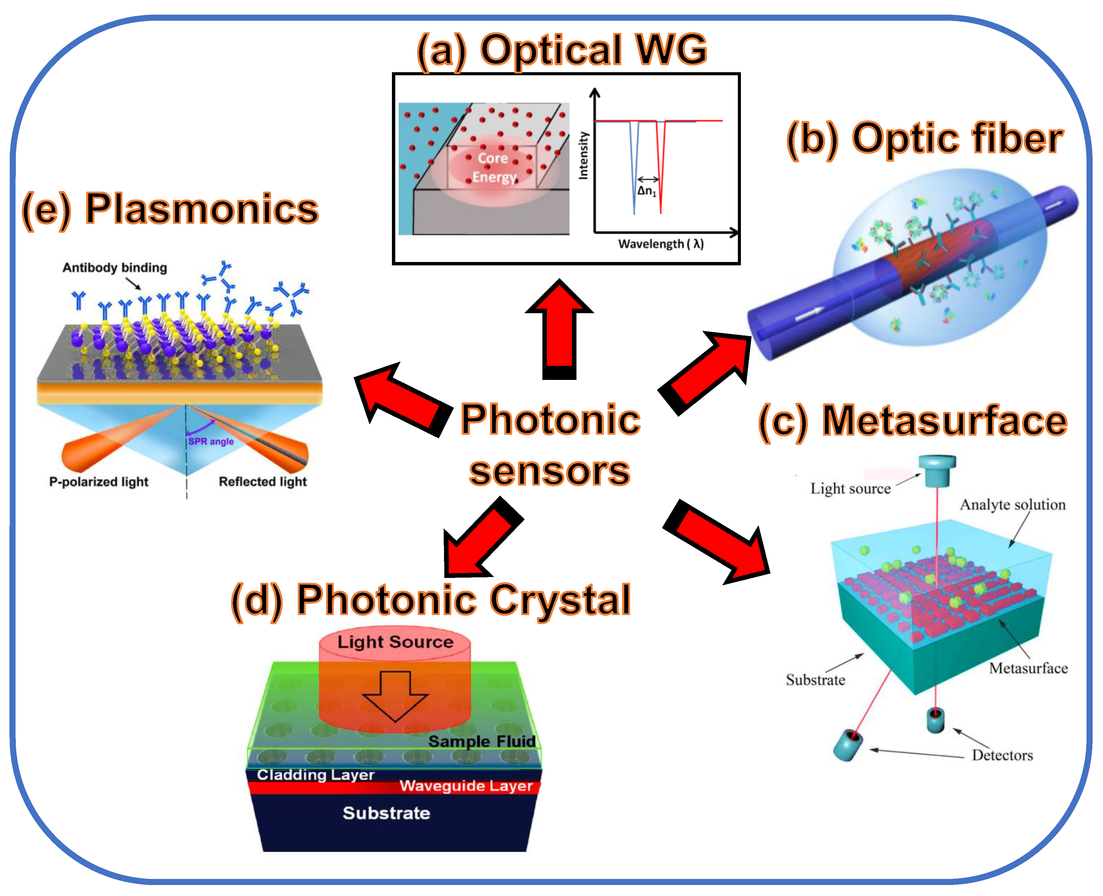
Submitted:
28 April 2023
Posted:
28 April 2023
You are already at the latest version
Abstract
Keywords:
1. Introduction
2. Optical Waveguide-Based Sensors
3. Optical Fiber-Based Sensors
4. Photonic Crystal-Based Sensors
5. Metasurface-Based Sensors
6. Plasmonic Sensors Based on Metal-Insulator-Metal Waveguide
7. Concluding Remarks
Author Contributions
Funding
Acknowledgments
Conflicts of Interest
Abbreviations
References
- Tan, Y.; Dai, D. Silicon microring resonators. J. Opt. 2018, 20, 054004. [Google Scholar] [CrossRef]
- A Butt, M.; Khonina, S.N.; Kazanskiy, N.L. A highly sensitive design of subwavelength grating double-slot waveguide microring resonator. Laser Phys. Lett. 2020, 17, 076201. [Google Scholar] [CrossRef]
- Homola, J. Surface Plasmon Resonance Sensors for Detection of Chemical and Biological Species. Chem. Rev. 2008, 108, 462–493. [Google Scholar] [CrossRef] [PubMed]
- Badri, S.H.; Gilarlue, M.M.; Farkoush, S.G.; Rhee, S.B. Reconfigurable bandpass optical filters based on subwavelength grating waveguides with a Ge 2 Sb 2 Te 5 cavity. JOSA B 2021, 38, 1283–1289. [Google Scholar] [CrossRef]
- Butt, M.A.; Khonina, S.N.; Kazanskiy, N.L. Plasmonic refractive index sensor based on metal–insulator-metal waveguides with high sensitivity. J. Mod. Opt. 2019, 66, 1038–1043. [Google Scholar] [CrossRef]
- Danaie, M.; Kiani, B. Design of a label-free photonic crystal refractive index sensor for biomedical applications. Photon- Nanostructures - Fundam. Appl. 2018, 31, 89–98. [Google Scholar] [CrossRef]
- Panda, A.; Devi, P.P. Photonic crystal biosensor for refractive index based cancerous cell detection. Opt. Fiber Technol. 2020, 54. [Google Scholar] [CrossRef]
- Derbali, J.; AbdelMalek, F.; Obayya, S.S.A.; Bouchriha, H.; Letizia, R. Design of a compact photonic crystal sensor. Opt. Quantum Electron. 2010, 42, 463–472. [Google Scholar] [CrossRef]
- Vijayalakshmi, D.; Manimegalai, C.T.; Ayyanar, N.; Nguyen, T.K.; Kalimuthu, K. Highly sensitive tri-path photonic crystal fiber plasmonic sensor based on hybrid layer of gold/platinum diselenide. Opt. Quantum Electron. 2021, 53, 1–17. [Google Scholar] [CrossRef]
- Islam, M.R.; Iftekher, A.N.M.; Hasan, K.R.; Nayen, J.; Bin Islam, S.; Hossain, A.; Mustafa, Z.; Tahsin, T. Design and numerical analysis of a gold-coated photonic crystal fiber based refractive index sensor. Opt. Quantum Electron. 2021, 53, 1–18. [Google Scholar] [CrossRef]
- Cooper, M.A. Label-free screening of bio-molecular interactions. Anal. Bioanal. Chem. 2003, 377, 834–842. [Google Scholar] [CrossRef]
- Anker, J.N.; Hall, W.P.; Lyandres, O.; Shah, N.C.; Zhao, J.; Van Duyne, R.P. Biosensing with plasmonic nanosensors. Nat. Mater. 2008, 7, 442–453. [Google Scholar] [CrossRef]
- Vollmer, F.; Arnold, S. Whispering-gallery-mode biosensing: label-free detection down to single molecules. Nat. Methods 2008, 5, 591–596. [Google Scholar] [CrossRef]
- Daniels, J.S.; Pourmand, N. Label-Free Impedance Biosensors: Opportunities and Challenges. Electroanalysis 2007, 19, 1239–1257. [Google Scholar] [CrossRef]
- Länge, K.; Rapp, B.E.; Rapp, M. Surface acoustic wave biosensors: a review. Anal. Bioanal. Chem. 2008, 391, 1509–1519. [Google Scholar] [CrossRef] [PubMed]
- Mandal, S.; Goddard, J.M.; Erickson, D. A multiplexed optofluidic biomolecular sensor for low mass detection. Lab A Chip 2009, 9, 2924–2932. [Google Scholar] [CrossRef] [PubMed]
- Martin, A.L.; Armani, D.K.; Yang, L.; Vahala, K.J. Replica-molded high-Q polymer microresonators. Opt. Lett. 2004, 29, 533–535. [Google Scholar] [CrossRef] [PubMed]
- Myers, F.B.; Lee, L.P. Innovations in optical microfluidic technologies for point-of-care diagnostics. Lab Chip 2008, 8, 2015–2031. [Google Scholar] [CrossRef]
- Butt, M.A.; Khonina, S.N.; Kazanskiy, N.L. Hybrid plasmonic waveguide-assisted Metal–Insulator–Metal ring resonator for refractive index sensing. J. Mod. Opt. 2018, 65, 1135–1140. [Google Scholar] [CrossRef]
- Mancuso, M.; Goddard, J.M.; Erickson, D. Nanoporous polymer ring resonators for biosensing. Opt. Express 2011, 20, 245–255. [Google Scholar] [CrossRef] [PubMed]
- Chiavaioli, F.; Baldini, F.; Tombelli, S.; Trono, C.; Giannetti, A. Biosensing with optical fiber gratings. Nanophotonics 2017, 6, 663–679. [Google Scholar] [CrossRef]
- Rodionov, S.; Remnev, M.; Klimov, V. Refractive index sensor based on all-dielectric gradient metasurface. Sens. Bio-Sens. Res. 2019, 22, 100263. [Google Scholar] [CrossRef]
- https://spie.org/news/wearable-photonics?SSO=1".
- Khan, Y.; Butt, M.A.; Kazanskiy, N.L.; Khonina, S.N. Numerical Study of Fabrication-Related Effects of the Structural-Profile on the Performance of a Dielectric Photonic Crystal-Based Fluid Sensor. Materials 2022, 15, 3277. [Google Scholar] [CrossRef]
- Ouyang, Q.; Zeng, S.; Jiang, L.; Hong, L.; Xu, G.; Dinh, X.-Q.; Qian, J.; He, S.; Qu, J.; Coquet, P.; et al. Sensitivity Enhancement of Transition Metal Dichalcogenides/Silicon Nanostructure-based Surface Plasmon Resonance Biosensor. Sci. Rep. 2016, 6, 28190. [Google Scholar] [CrossRef]
- Butt, M.A. , Nguyen, H.D., Ródenas, A., Romero, C., Moreno, P., de Aldana, J.R.V., Aguiló, M., Solé, R.M., Pujol, M.C. and Díaz, F. Low-repetition rate femtosecond laser writing of optical waveguides in KTP crystals: analysis of anisotropic refractive index changes. Opt. Express 2015, 23, 15343–15355. [Google Scholar] [CrossRef] [PubMed]
- Belt, M.; Bovington, J.; Moreira, R.; Bauters, J.F.; Heck, M.J.R.; Barton, J.S.; Bowers, J.E.; Blumenthal, D.J. Sidewall gratings in ultra-low-loss Si_3N_4 planar waveguides. Opt. Express 2013, 21, 1181–1188. [Google Scholar] [CrossRef]
- Albert, J.; Lit, J.W.Y. Full modeling of field-assisted ion exchange for graded index buried channel optical waveguides. Appl. Opt. 1990, 29, 2798–2804. [Google Scholar] [CrossRef] [PubMed]
- Butt, M.A. , Khonina, S.N. and Kazanskiy, N.L. Modelling of Rib channel waveguides based on silicon-on-sapphire at 4.67 μm wavelength for evanescent field gas absorption sensor. Optik 2018, 168, 692–697. [Google Scholar] [CrossRef]
- Butt, M.A.; Khonina, S.N.; Kazanskiy, N.L. Silicon on silicon dioxide slot waveguide evanescent field gas absorption sensor. J. Mod. Opt. 2017, 65, 174–178. [Google Scholar] [CrossRef]
- Kazanskiy, N.L.; Butt, M.A.; Khonina, S.N. Optical Computing: Status and Perspectives. Nanomaterials 2022, 12, 2171. [Google Scholar] [CrossRef]
- Zwerver, A.M.J.; Krähenmann, T.; Watson, T.F.; Lampert, L.; George, H.C.; Pillarisetty, R.; Bojarski, S.A.; Amin, P.; Amitonov, S.V.; Boter, J.M.; et al. Qubits made by advanced semiconductor manufacturing. Nat. Electron. 2022, 5, 184–190. [Google Scholar] [CrossRef]
- Alexoudi, T.; Kanellos, G.T.; Pleros, N. Optical RAM and integrated optical memories: a survey. Light. Sci. Appl. 2020, 9, 1–16. [Google Scholar] [CrossRef] [PubMed]
- Washburn, A.L. and Bailey, R.C. Photonics-on-a-chip: recent advances in integrated waveguides as enabling detection elements for real-world, lab-on-a-chip biosensing applications. Analyst 2011, 136, 227–236. [Google Scholar] [CrossRef]
- Tai, H. , Tanaka, H. and Yoshino, T. Fiber-optic evanescent-wave methane-gas sensor using optical absorption for the 3.392-μm line of a He–Ne laser. Optics letters 1987, 12, 437–439. [Google Scholar]
- Sekimoto, S.; Nakagawa, H.; Okazaki, S.; Fukuda, K.; Asakura, S.; Shigemori, T.; Takahashi, S. A fiber-optic evanescent-wave hydrogen gas sensor using palladium-supported tungsten oxide. Sens. Actuators B: Chem. 2000, 66, 142–145. [Google Scholar] [CrossRef]
- Huang, Y. , Kalyoncu, S. K., Zhao, Q., Torun, R. and Boyraz, O. Silicon-on-sapphire waveguides design for mid-IR evanescent field absorption gas sensors. Optics Communications 2014, 313, 186–194. [Google Scholar]
- Khonina, S.N.; Kazanskiy, N.L.; Butt, M.A. Evanescent Field Ratio Enhancement of a Modified Ridge Waveguide Structure for Methane Gas Sensing Application. IEEE Sens. J. 2020, 20, 8469–8476. [Google Scholar] [CrossRef]
- Kazanskiy, N.L. , Butt, M. A. and Kaźmierczak, A. Why slot and hybrid plasmonic waveguides are ideal candidates for sensing applications?. Optoelectronics and Advanced Materials Rapid Communications 2021, 15, 195–206. [Google Scholar]
- Pelli, S.; Righini, G.C.; Scaglione, A.; Guglielmi, M.; Martucci, A. Direct laser writing of ridge optical waveguides in silica-titania glass sol-gel films. Opt. Mater. 1996, 5, 119–126. [Google Scholar] [CrossRef]
- Butt, M.A. , Khonina, S. N. and Kazanskiy, N.L.. Ultrashort inverted tapered silicon ridge-to-slot waveguide coupler at 1.55 µm and 3.392 µm wavelength. Applied Optics 2020, 59, 7821–7828. [Google Scholar]
- Tayoub, H.; Hocini, A.; Harhouz, A. HIGH-SENSITIVE MID-INFRARED PHOTONIC CRYSTAL SENSOR USING SLOTTED-WAVEGUIDE COUPLED-CAVITY. Prog. Electromagn. Res. M 2021, 105, 45–54. [Google Scholar] [CrossRef]
- Yuan, D.; Dong, Y.; Liu, Y.; Li, T. Mach-Zehnder Interferometer Biochemical Sensor Based on Silicon-on-Insulator Rib Waveguide with Large Cross Section. Sensors 2015, 15, 21500–21517. [Google Scholar] [CrossRef] [PubMed]
- Heinsalu, S.; Isogai, Y.; Matsushima, Y.; Ishikawa, H.; Utaka, K. Record-high sensitivity compact multi-slot sub-wavelength Bragg grating refractive index sensor on SOI platform. Opt. Express 2020, 28, 28126–28139. [Google Scholar] [CrossRef] [PubMed]
- Prabhathan, P.; Murukeshan, V.M.; Jing, Z.; Ramana, P.V. Compact SOI nanowire refractive index sensor using phase shifted Bragg grating. Opt. Express 2009, 17, 15330–15341. [Google Scholar] [CrossRef] [PubMed]
- Kehl, F. , Bischof, D. , Michler, M., Keka, M. and Stanley, R. Design of a label-free, distributed Bragg grating resonator based dielectric waveguide biosensor. Photonics 2015, 2, 124–138. [Google Scholar]
- Sahu, S.; Ali, J.; Singh, G. Refractive index biosensor using sidewall gratings in dual-slot waveguide. Opt. Commun. 2017, 402, 408–412. [Google Scholar] [CrossRef]
- Liu, L.; Hu, Z.; Ye, M.; Yu, Z.; Ma, C.; Li, J. On-Chip Refractive Index Sensor With Ultra-High Sensitivity Based on Sub-Wavelength Grating Racetrack Microring Resonators and Vernier Effect. IEEE Photon- J. 2022, 14, 1–7. [Google Scholar] [CrossRef]
- De Leonardis, F.; Campanella, C.E.; Troia, B.; Perri, A.G.; Passaro, V.M.N. Performance of SOI Bragg Grating Ring Resonator for Nonlinear Sensing Applications. Sensors 2014, 14, 16017–16034. [Google Scholar] [CrossRef]
- Zhao, C.Y.; Zhang, L.; Zhang, C.M. Compact SOI optimized slot microring coupled phase-shifted Bragg grating resonator for sensing. Opt. Commun. 2018, 414, 212–216. [Google Scholar] [CrossRef]
- Guider, R. , Gandolfi, D. , Chalyan, T., Pasquardini, L., Samusenko, A., Pederzolli, C., Pucker, G. and Pavesi, L. Sensitivity and limit of detection of biosensors based on ring resonators. Sensing and bio-sensing research 2015, 6, 99–102. [Google Scholar]
- Di Falco, A. , O’faolain, L. and Krauss, T.F. Chemical sensing in slotted photonic crystal heterostructure cavities. Applied physics letters 2009, 94, 063503. [Google Scholar]
- Claes, T.; Bogaerts, W.; Bienstman, P. Experimental characterization of a silicon photonic biosensor consisting of two cascaded ring resonators based on the Vernier-effect and introduction of a curve fitting method for an improved detection limit. Opt. Express 2010, 18, 22747–22761. [Google Scholar] [CrossRef] [PubMed]
- Chow, E.; Grot, A.; Mirkarimi, L.W.; Sigalas, M.; Girolami, G. Ultracompact biochemical sensor built with two-dimensional photonic crystal microcavity. Opt. Lett. 2004, 29, 1093–1095. [Google Scholar] [CrossRef] [PubMed]
- Butt, M.A. , Khonina, S. N. and Kazanskiy, N.L. Device performance of standard strip, slot and hybrid plasmonic μ-ring resonator: a comparative study. Waves in Random and Complex Media 2021, 31, 2397–2406. [Google Scholar]
- Mirsadeghi, S.H.; Schelew, E.; Young, J.F. Photonic crystal slot-microcavity circuit implemented in silicon-on-insulator: High Q operation in solvent without undercutting. Appl. Phys. Lett. 2013, 102. [Google Scholar] [CrossRef]
- Carlborg, C.F.; Gylfason, K.B.; Kaźmierczak, A.; Dortu, F.; Polo, M.J.B.; Catala, A.M.; Kresbach, G.M.; Sohlström, H.; Moh, T.; Vivien, L.; et al. A packaged optical slot-waveguide ring resonator sensor array for multiplex label-free assays in labs-on-chips. Lab A Chip 2009, 10, 281–290. [Google Scholar] [CrossRef] [PubMed]
- Claes, T.; Molera, J.G.; De Vos, K.; Schacht, E.; Baets, R.; Bienstman, P. Label-Free Biosensing With a Slot-Waveguide-Based Ring Resonator in Silicon on Insulator. IEEE Photon- J. 2009, 1, 197–204. [Google Scholar] [CrossRef]
- Xing, P.; Viegas, J. Broadband CMOS-compatible SOI temperature insensitive Mach-Zehnder interferometer. Opt. Express 2015, 23, 24098–107. [Google Scholar] [CrossRef]
- Wang, C.; Yi, P.; Li, J.; Dong, H.; Chen, C.; Zhang, D.; Shen, H.; Fu, B. Polymer Optical Waveguide Grating-Based Biosensor to Detect Effective Drug Concentrations of Ginkgolide A for Inhibition of PMVEC Apoptosis. Biosensors 2021, 11, 264. [Google Scholar] [CrossRef]
- Wang, X.; Xu, Z.; Lu, N.; Zhu, J.; Jin, G. Ultracompact refractive index sensor based on microcavity in the sandwiched photonic crystal waveguide structure. Opt. Commun. 2008, 281, 1725–1731. [Google Scholar] [CrossRef]
- Hiltunen, M.; Hiltunen, J.; Stenberg, P.; Aikio, S.; Kurki, L.; Vahimaa, P.; Karioja, P. Polymeric slot waveguide interferometer for sensor applications. Opt. Express 2014, 22, 7229–7237. [Google Scholar] [CrossRef] [PubMed]
- Huang, L.; Tian, H.; Zhou, J.; Liu, Q.; Zhang, P.; Ji, Y. Label-free optical sensor by designing a high-Q photonic crystal ring–slot structure. Opt. Commun. 2014, 335, 73–77. [Google Scholar] [CrossRef]
- Butt, M.A.; Kazanskiy, N.L.; Khonina, S.N. Modal Characteristics of Refractive Index Engineered Hybrid Plasmonic Waveguide. IEEE Sens. J. 2020, 20, 9779–9786. [Google Scholar] [CrossRef]
- Ahmadi, L.; Hiltunen, M.; Stenberg, P.; Hiltunen, J.; Aikio, S.; Roussey, M.; Saarinen, J.; Honkanen, S. Hybrid layered polymer slot waveguide Young interferometer. Opt. Express 2016, 24, 10275–85. [Google Scholar] [CrossRef]
- Zhao, C.Y.; Chen, P.Y.; Zhang, L. Numerical analysis of effective refractive index sensor based on slot micro-ring and Bragg grating. Int. J. Mod. Phys. B 2019, 33. [Google Scholar] [CrossRef]
- Butt, M.; Khonina, S.; Kazanskiy, N. Plasmonics: A Necessity in the Field of Sensing-A Review (Invited). Fiber Integr. Opt. 2021, 40, 14–47. [Google Scholar] [CrossRef]
- Mowbray, S.E.; Amiri, A.M. A Brief Overview of Medical Fiber Optic Biosensors and Techniques in the Modification for Enhanced Sensing Ability. Diagnostics 2019, 9, 23. [Google Scholar] [CrossRef]
- Anderson, G.P.; King, K.D.; Gaffney, K.L.; Johnson, L.H. Multi-analyte interrogation using the fiber optic biosensor. Biosens. Bioelectron. 2000, 14, 771–777. [Google Scholar] [CrossRef]
- Butt, M.A.; Kazanskiy, N.L.; Khonina, S.N. Label-free detection of ambient refractive index based on plasmonic Bragg gratings embedded resonator cavity sensor. J. Mod. Opt. 2019, 66, 1920–1925. [Google Scholar] [CrossRef]
- Binfeng, Y.; Guohua, H.; Ruohu, Z.; Yiping, C. Design of a compact and high sensitive refractive index sensor base on metal-insulator-metal plasmonic Bragg grating. Opt. Express 2014, 22, 28662–28670. [Google Scholar] [CrossRef]
- Passaro, V.M.N.; Loiacono, R.; D'Amico, G.; De Leonardis, F. Design of Bragg Grating Sensors Based on Submicrometer Optical Rib Waveguides in SOI. IEEE Sens. J. 2008, 8, 1603–1611. [Google Scholar] [CrossRef]
- Klimov, N.N.; Mittal, S.; Berger, M.; Ahmed, Z. On-chip silicon waveguide Bragg grating photonic temperature sensor. Opt. Lett. 2015, 40, 3934–3936. [Google Scholar] [CrossRef] [PubMed]
- Hill, K.; Meltz, G. Fiber Bragg grating technology fundamentals and overview. J. Light. Technol. 1997, 15, 1263–1276. [Google Scholar] [CrossRef]
- Hill, K.O.; Fujii, Y.; Johnson, D.C.; Kawasaki, B.S. Photosensitivity in optical fiber waveguides: Application to reflection filter fabrication. Appl. Phys. Lett. 1978, 32, 647–649. [Google Scholar] [CrossRef]
- Kersey, A.D. , Davis, M. A., Patrick, H.J., LeBlanc, M., Koo, K.P., Askins, C.G., Putnam, M.A. and Friebele, E.J. Fiber grating sensors. Journal of lightwave technology 1997, 15, 442–1463. [Google Scholar]
- H. Alemohammad, R. H. Alemohammad, R. Liang, D. Yilman, A. Azhari, K. Mathers, C. Chang, B. Chan and M. Pope, "Fiber optic sensors for harsh environments: Environmental, hydrogeological, and chemical sensing applications," in 26th International Conference on Optical Fiber Sensors, Lausanne Switzerland, 24-. 28 September.
- Qiao, X.; Shao, Z.; Bao, W.; Rong, Q. Fiber Bragg Grating Sensors for the Oil Industry. Sensors 2017, 17, 429. [Google Scholar] [CrossRef] [PubMed]
- H. Linzi, Z. H. Linzi, Z. Wu, X. Zhang, F. Qiangqiang, X. Jian, T. Yong, G. Tuan and G. Bai-Ou, "High sensitive thrombin protein detection by plasmonic tilted fiber grating biosensor," in Proceedings of the Workshop on Specialty Optical Fibers and their applications, Hong Kong, China, 4-. 6 November.
- Arghir, I.; Spasic, D.; Verlinden, B.E.; Delport, F.; Lammertyn, J. Improved surface plasmon resonance biosensing using silanized optical fibers. Sens. Actuators B: Chem. 2015, 216, 518–526. [Google Scholar] [CrossRef]
- Coelho, L.; de Almeida, J.M.M.M.; Santos, J.L.; Jorge, P.A.d.S.; Martins, M.C.L.; Viegas, D.; Queirós, R.B. Aptamer-based fiber sensor for thrombin detection. J. Biomed. Opt. 2016, 21, 087005–087005. [Google Scholar] [CrossRef]
- Zhou, Z.; Xu, Y.; Qiao, C.; Liu, L.; Jia, Y. A novel low-cost gas sensor for CO2 detection using polymer-coated fiber Bragg grating. Sens. Actuators B: Chem. 2021, 332, 129482. [Google Scholar] [CrossRef]
- Xu, Y.; Lu, P.; Gao, S.; Xiang, D.; Mihailov, S.; Bao, X. Optical fiber random grating-based multiparameter sensor. Opt. Lett. 2015, 40, 5514–5517. [Google Scholar] [CrossRef]
- Maaskant, R.; Alavie, T.; Measures, R.; Tadros, G.; Rizkalla, S.; Guha-Thakurta, A. Fiber-optic Bragg grating sensors for bridge monitoring. Cem. Concr. Compos. 1997, 19, 21–33. [Google Scholar] [CrossRef]
- Kretschmann, E. and Raether, H. Radiative decay of non radiative surface plasmons excited by light. Zeitschrift für Naturforschung A 1968, 23, 2135–2136. [Google Scholar]
- Otto, A. Excitation of nonradiative surface plasma waves in silver by the method of frustrated total reflection. Zeitschrift für Physik A Hadrons and nuclei 1968, 216, 398–410. [Google Scholar] [CrossRef]
- Pevec, S.; Donlagic, D. Miniature fiber-optic Fabry-Perot refractive index sensor for gas sensing with a resolution of 5x10⁻⁹ RIU. Opt. Express 2018, 26, 23868–23882. [Google Scholar] [CrossRef] [PubMed]
- Skorobogatiy, M.; Kabashin, A.V. Photon crystal waveguide-based surface plasmon resonance biosensor. Appl. Phys. Lett. 2006, 89. [Google Scholar] [CrossRef]
- Piliarik, M.; Homola, J.; Manı́ková, Z.; Čtyroký, J. Surface plasmon resonance sensor based on a single-mode polarization-maintaining optical fiber. Sens. Actuators B: Chem. 2003, 90, 236–242. [Google Scholar] [CrossRef]
- Gupta, B.; Sharma, A.K. Sensitivity evaluation of a multi-layered surface plasmon resonance-based fiber optic sensor: a theoretical study. Sens. Actuators B: Chem. 2005, 107, 40–46. [Google Scholar] [CrossRef]
- Jorgenson, R.C.; Yee, S.S. A fiber-optic chemical sensor based on surface plasmon resonance. Sens. Actuators B Chem. 1993, 12, 213–220. [Google Scholar] [CrossRef]
- Lin, Y.-C. Comparison of Transmission-Type and Reflection-Type Surface Plasmon Resonance Based Fiber-Optic Sensor. 2016 International Symposium on Computer, Consumer and Control (IS3C). LOCATION OF CONFERENCE, ChinaDATE OF CONFERENCE; pp. 436–438.
- Singh, S.; Mishra, S.K.; Gupta, B.D. Sensitivity enhancement of a surface plasmon resonance based fibre optic refractive index sensor utilizing an additional layer of oxides. Sens. Actuators A: Phys. 2013, 193, 136–140. [Google Scholar] [CrossRef]
- Fontana, E.; Dulman, H.; Doggett, D.; Pantell, R. Surface plasmon resonance on a single mode optical fiber. IEEE Trans. Instrum. Meas. 1998, 47, 168–173. [Google Scholar] [CrossRef]
- Mao, P.; Luo, Y.; Chen, X.; Fang, J.; Huang, H.; Chen, C.; Peng, S.; Zhang, J.; Tang, J.; Lu, H.; et al. Design and optimization of multimode fiber sensor based on surface plasmon resonance. 14th International Conference on Numerical Simulation of Optoelectronic Devices (NUSOD 2014). LOCATION OF CONFERENCE, SpainDATE OF CONFERENCE; pp. 119–120.
- Hoseinian, M.S.; Bolorizadeh, M.A. Design and Simulation of a Highly Sensitive SPR Optical Fiber Sensor. Photon- Sens. 2018, 9, 33–42. [Google Scholar] [CrossRef]
- Xie, T.; He, Y.; Yang, Y.; Zhang, H.; Xu, Y. Highly Sensitive Surface Plasmon Resonance Sensor Based on Graphene-Coated U-shaped Fiber. Plasmonics 2020, 16, 205–213. [Google Scholar] [CrossRef]
- Verma, R.K. and Gupta, B. D. Theoretical modelling of a bi-dimensional U-shaped surface plasmon resonance based fibre optic sensor for sensitivity enhancement. Journal of Physics D: Applied Physics 2008, 41, 095106. [Google Scholar]
- Yu, H.; Chong, Y.; Zhang, P.; Ma, J.; Li, D. A D-shaped fiber SPR sensor with a composite nanostructure of MoS2-graphene for glucose detection. Talanta 2020, 219, 121324. [Google Scholar] [CrossRef] [PubMed]
- Arasu, P.T.; Al-Qazwini, Y.; Onn, B.I.; Noor, A.S.M. Fiber Bragg grating based surface plasmon resonance sensor utilizing FDTD for alcohol detection applications. 2012 IEEE 3rd International Conference on Photonics (ICP). LOCATION OF CONFERENCE, MalaysiaDATE OF CONFERENCE; pp. 93–97.
- Kim, Y.-C.; Peng, W.; Banerji, S.; Booksh, K.S. Tapered fiber optic surface plasmon resonance sensor for analyses of vapor and liquid phases. Opt. Lett. 2005, 30, 2218–2220. [Google Scholar] [CrossRef] [PubMed]
- Navarrete, M.-C.; Díaz-Herrera, N.; González-Cano, A.; Esteban. Surface plasmon resonance in the visible region in sensors based on tapered optical fibers. Sens. Actuators B: Chem. 2014, 190, 881–885. [Google Scholar] [CrossRef]
- Choi, W.J.; Jeon, D.I.; Ahn, S.-G.; Yoon, J.-H.; Kim, S.; Lee, B.H. Full-field optical coherence microscopy for identifying live cancer cells by quantitative measurement of refractive index distribution. Opt. Express 2010, 18, 23285–23295. [Google Scholar] [CrossRef] [PubMed]
- Yasli, A. Cancer detection with surface plasmon resonance-based photonic crystal fiber biosensor. Plasmonics 2021, 16, 1605–1612. [Google Scholar] [CrossRef]
- Mollah, A.; Yousufali; Ankan, I. M.; Rahman, M.; Sarker, H.; Chakrabarti, K. Twin core photonic crystal fiber refractive index sensor for early detection of blood cancer. Sens. Bio-Sens. Res. 2020, 29, 100344. [Google Scholar] [CrossRef]
- Ayyanar, N.; Raja, G.T.; Sharma, M.; Kumar, D.S. Photonic Crystal Fiber-Based Refractive Index Sensor for Early Detection of Cancer. IEEE Sens. J. 2018, 18, 7093–7099. [Google Scholar] [CrossRef]
- Mishra, G.P.; Kumar, D.; Chaudhary, V.S.; Murmu, G. Cancer cell detection by a heart-shaped dual-core photonic crystal fiber sensor. Appl. Opt. 2020, 59, 10321–10329. [Google Scholar] [CrossRef]
- Buczynski, R.J.A.P.P.S.A. Photonic crystal fibers. Acta Physica Polonica A 2004, 106, 141–167. [Google Scholar] [CrossRef]
- Shuai, B.; Xia, L.; Zhang, Y.; Liu, D. A multi-core holey fiber based plasmonic sensor with large detection range and high linearity. Opt. Express 2012, 20, 5974–5986. [Google Scholar] [CrossRef] [PubMed]
- Zhao, L.; Han, H.; Luan, N.; Liu, J.; Song, L.; Hu, Y. A Temperature Plasmonic Sensor Based on a Side Opening Hollow Fiber Filled with High Refractive Index Sensing Medium. Sensors 2019, 19, 3730. [Google Scholar] [CrossRef] [PubMed]
- Han, H.; Hou, D.; Zhao, L.; Luan, N.; Song, L.; Liu, Z.; Lian, Y.; Liu, J.; Hu, Y. A Large Detection-Range Plasmonic Sensor Based on An H-Shaped Photonic Crystal Fiber. Sensors 2020, 20, 1009. [Google Scholar] [CrossRef]
- Li, C.; Li, Z.; Li, S.; Zhang, Y.; Sun, B.; Yu, Y.; Ren, H.; Jiang, S.; Yue, W. LSPR optical fiber biosensor based on a 3D composite structure of gold nanoparticles and multilayer graphene films. Opt. Express 2020, 28, 6071–6083. [Google Scholar] [CrossRef] [PubMed]
- Yunianto, M.; Permata, A.N.; Eka, D.; Ariningrum, D.; Wahyuningsih, S.; Marzuki, A. Design of a Fiber Optic Biosensor for Cholesterol Detection in Human Blood. 2017, 176, 012014. [CrossRef]
- Cheng, Y.; Wang, Y.; Song, Z.; Lei, J. High-sensitivity optical fiber temperature sensor based on a dual-loop optoelectronic oscillator with the Vernier effect. Opt. Express 2020, 28, 35264–35271. [Google Scholar] [CrossRef]
- Cao, H. , Li, D. , Zhou, K. and Chen, Y. Demonstration of a ZnO-nanowire-based nanograting temperature sensor. Photonic Sensors 2023, 13, 230123. [Google Scholar]
- Zhang, H.; Xie, Z.; Yan, H.; Li, P.; Wang, P.; Han, D. High sensitivity and large measurement range magnetic field micro-nano fiber sensor based on Mach-Zehnder interference. Opt. Laser Technol. 2022, 156. [Google Scholar] [CrossRef]
- Selvendran, S.; Susheel, A.; Tarun, P.V.; Muthu, K.E.; Raja, A.S. A novel surface plasmon based photonic crystal fiber sensor. Opt. Quantum Electron. 2020, 52, 1–12. [Google Scholar] [CrossRef]
- Melo, A.A.; Santiago, M.F.; Silva, T.B.; Moreira, C.S.; Cruz, R.M. Investigation of a D-Shaped Optical Fiber Sensor with Graphene Overlay. IFAC-Pap. 2018, 51, 309–314. [Google Scholar] [CrossRef]
- Tien, C.-L.; Lin, H.-Y.; Su, S.-H. High Sensitivity Refractive Index Sensor by D-Shaped Fibers and Titanium Dioxide Nanofilm. Adv. Condens. Matter Phys. 2018, 2018, 1–6. [Google Scholar] [CrossRef]
- Larrión, B.; Hernáez, M.; Arregui, F.J.; Goicoechea, J.; Bravo, J.; Matías, I.R. Photonic Crystal Fiber Temperature Sensor Based on Quantum Dot Nanocoatings. J. Sens. 2009, 2009, 1–6. [Google Scholar] [CrossRef]
- Haque, E.; Hossain, A.; Ahmed, F.; Namihira, Y. Surface Plasmon Resonance Sensor Based on Modified $D$ -Shaped Photonic Crystal Fiber for Wider Range of Refractive Index Detection. IEEE Sens. J. 2018, 18, 8287–8293. [Google Scholar] [CrossRef]
- Wu, T.; Shao, Y.; Wang, Y.; Cao, S.; Cao, W.; Zhang, F.; Liao, C.; He, J.; Huang, Y.; Hou, M.; et al. Surface plasmon resonance biosensor based on gold-coated side-polished hexagonal structure photonic crystal fiber. Opt. Express 2017, 25, 20313–20322. [Google Scholar] [CrossRef]
- Paul, A.K. Design and analysis of photonic crystal fiber plasmonic refractive Index sensor for condition monitoring of transformer oil. OSA Continuum 2020, 3, 2253–2263. [Google Scholar] [CrossRef]
- Shafkat, A.; Rashed, A.N.Z.; El-Hageen, H.M.; Alatwi, A.M. Design and analysis of a single elliptical channel photonic crystal fiber sensor for potential malaria detection. J. Sol-Gel Sci. Technol. 2021, 98, 202–211. [Google Scholar] [CrossRef]
- Shen, H.; Wang, Z.; Wu, Y.; Yang, B. One-dimensional photonic crystals: fabrication, responsiveness and emerging applications in 3D construction. RSC Adv. 2015, 6, 4505–4520. [Google Scholar] [CrossRef]
- A Butt, M.; Kazanskiy, N.L. Two-dimensional photonic crystal heterostructure for light steering and TM-polarization maintaining applications. Laser Phys. 2021, 31, 036201. [Google Scholar] [CrossRef]
- Butt, M.; Khonina, S.; Kazanskiy, N. 2D-Photonic crystal heterostructures for the realization of compact photonic devices. Photon- Nanostructures - Fundam. Appl. 2021, 44. [Google Scholar] [CrossRef]
- Yu, S.-P.; Muniz, J.A.; Hung, C.-L.; Kimble, H.J. Two-dimensional photonic crystals for engineering atom–light interactions. Proc. Natl. Acad. Sci. 2019, 116, 12743–12751. [Google Scholar] [CrossRef] [PubMed]
- Chen, C.-W.; Hou, C.-T.; Li, C.-C.; Jau, H.-C.; Wang, C.-T.; Hong, C.-L.; Guo, D.-Y.; Wang, C.-Y.; Chiang, S.-P.; Bunning, T.J.; et al. Large three-dimensional photonic crystals based on monocrystalline liquid crystal blue phases. Nat. Commun. 2017, 8, 1–8. [Google Scholar] [CrossRef]
- Wang, Z.; Liu, D. Special kind of photonic crystals with omnidirectional bandgaps. J. Opt. Soc. Am. B 2006, 23, 2601–2604. [Google Scholar] [CrossRef]
- Zu, P.; Chan, C.C.; Jin, Y.; Gong, T.; Zhang, Y.; Chen, L.H.; Dong, X. A Temperature-Insensitive Twist Sensor by Using Low-Birefringence Photonic-Crystal-Fiber-Based Sagnac Interferometer. IEEE Photon- Technol. Lett. 2011, 23, 920–922. [Google Scholar] [CrossRef]
- Dinodiya, S.; Suthar, B.; Bhargava, A. Photonic crystal sensors: Physics and applications. 2ND INTERNATIONAL CONFERENCE ON CONDENSED MATTER AND APPLIED PHYSICS (ICC 2017). LOCATION OF CONFERENCE, IndiaDATE OF CONFERENCE; p. 060016.
- Taverne, M.P.C.; Ho, Y.-L.D.; Zheng, X.; Chen, L.; Fang, C.-H.N.; Rarity, J. Strong light confinement in rod-connected diamond photonic crystals. Opt. Lett. 2018, 43, 5202–5205. [Google Scholar] [CrossRef]
- Scullion, M.; Di Falco, A.; Krauss, T. Slotted photonic crystal cavities with integrated microfluidics for biosensing applications. Biosens. Bioelectron. 2011, 27, 101–105. [Google Scholar] [CrossRef] [PubMed]
- Zlatanovic, S.; Mirkarimi, L.W.; Sigalas, M.M.; Bynum, M.A.; Chow, E.; Robotti, K.M.; Burr, G.W.; Esener, S.; Grot, A. Photonic crystal microcavity sensor for ultracompact monitoring of reaction kinetics and protein concentration. Sens. Actuators B: Chem. 2009, 141, 13–19. [Google Scholar] [CrossRef]
- Sharma, V.; Kalyani, V.L. Design Two Dimensional Nanocavity Photonic Crystal Biosensor Detection in Malaria. Int. J. Emerg. Res. Manag. Technol. 2018, 6, 16–20. [Google Scholar] [CrossRef]
- Bendib, S. and Bendib, C. Photonic crystals for malaria detection. J. Biosens. Bioelectron 2018, 9, 1000257. [Google Scholar]
- Kassa-Baghdouche, L.; Cassan, E. Mid-infrared gas sensor based on high-Q/V point-defect photonic crystal nanocavities. Opt. Quantum Electron. 2020, 52, 1–13. [Google Scholar] [CrossRef]
- Jágerská, J.; Zhang, H.; Diao, Z.; Le Thomas, N.; Houdré, R. Refractive index sensing with an air-slot photonic crystal nanocavity. Opt. Lett. 2010, 35, 2523–2525. [Google Scholar] [CrossRef] [PubMed]
- Zhao, H.-J. High sensitivity refractive index gas sensing enhanced by surface plasmon resonance with nano-cavity antenna array. Chin. Phys. B 2012, 21, 087104. [Google Scholar] [CrossRef]
- Wang, L. , Sang, T. , Li, J., Zhou, J., Wang, B. and Wang, Y. High-sensitive transmission type of gas sensor based on guided-mode resonance in coupled gratings. Journal of Modern optics 2018, 65, 1601–1608. [Google Scholar]
- Chen, Y.; Dong, J.; Liu, T.; Zhu, Q.; Chen, W. Refractive index sensing performance analysis of photonic crystal containing graphene based on optical Tamm state. Mod. Phys. Lett. B 2016, 30. [Google Scholar] [CrossRef]
- Wang, G.; Lu, Y.; Duan, L.; Yao, J. A Refractive Index Sensor Based on PCF With Ultra-Wide Detection Range. IEEE J. Sel. Top. Quant. Electron. 2021, 27, 1–8. [Google Scholar] [CrossRef]
- Singh, S.; Prajapati, Y.K. Highly sensitive refractive index sensor based on D-shaped PCF with gold-graphene layers on the polished surface. Appl. Phys. A 2019, 125, 437. [Google Scholar] [CrossRef]
- Qin, W. , Li, S. G., Xue, J.R., Xin, X.J. and Zhang, L. Numerical analysis of a photonic crystal fiber based on two polarized modes for biosensing applications. Chinese Physics B 2013, 22, 074213. [Google Scholar]
- Shakya, A.K.; Singh, S. Design of dual polarized tetra core PCF based plasmonic RI sensor for visible-IR spectrum. Opt. Commun. 2020, 478, 126372. [Google Scholar] [CrossRef]
- Paul, A.K.; Sarkar, A.K.; Rahman, A.B.S.; Khaleque, A. Twin Core Photonic Crystal Fiber Plasmonic Refractive Index Sensor. IEEE Sens. J. 2018, 18, 5761–5769. [Google Scholar] [CrossRef]
- Fu, Y.-L.; Deng, C.-S.; Ma, S.-S. Design and analysis of refractive index sensors based on slotted photonic crystal nanobeam cavities with sidewall gratings. Appl. Opt. 2020, 59, 896–903. [Google Scholar] [CrossRef]
- Fan, Z. Surface plasmon resonance refractive index sensor based on photonic crystal fiber covering nano-ring gold film. Opt. Fiber Technol. 2019, 50, 194–199. [Google Scholar] [CrossRef]
- Rifat, A.A. , Mahdiraji, G. A., Shee, Y.G., Shawon, M.J. and Adikan, F.M. A novel photonic crystal fiber biosensor using surface plasmon resonance. Procedia engineering 2016, 140, 1–7. [Google Scholar]
- Li, D.; Zhang, W.; Liu, H.; Hu, J.; Zhou, G. High Sensitivity Refractive Index Sensor Based on Multicoating Photonic Crystal Fiber With Surface Plasmon Resonance at Near-Infrared Wavelength. IEEE Photon- J. 2017, 9, 1–8. [Google Scholar] [CrossRef]
- Otupiri, R. , Akowuah, E. K., Haxha, S., Ademgil, H., AbdelMalek, F. and Aggoun, A. A novel birefrigent photonic crystal fiber surface plasmon resonance biosensor. IEEE Photonics Journal 2014, 6, 1–11. [Google Scholar]
- Olyaee, S.; Najafgholinezhad, S.; Banaei, H.A. Four-channel label-free photonic crystal biosensor using nanocavity resonators. Photon- Sens. 2013, 3, 231–236. [Google Scholar] [CrossRef]
- Kurt, H.; Erim, M.N.; Erim, N. Various photonic crystal bio-sensor configurations based on optical surface modes. Sens. Actuators B: Chem. 2012, 165, 68–75. [Google Scholar] [CrossRef]
- Dündar, M.A.; Ryckebosch, E.C.; Nötzel, R.; Karouta, F.; van Ijzendoorn, L.J.; van der Heijden, R.W. Sensitivities of InGaAsP photonic crystal membrane nanocavities to hole refractive index. Opt. Express 2010, 18, 4049–4056. [Google Scholar] [CrossRef]
- Kang, P.; Schein, P.; Serey, X.; O’dell, D.; Erickson, D. Nanophotonic detection of freely interacting molecules on a single influenza virus. Sci. Rep. 2015, 5, 12087. [Google Scholar] [CrossRef]
- Baker, J.E.; Sriram, R.; Miller, B.L. Recognition-mediated particle detection under microfluidic flow with waveguide-coupled 2D photonic crystals: towards integrated photonic virus detectors. Lab A Chip 2017, 17, 1570–1577. [Google Scholar] [CrossRef]
- Lee, M.R.; Fauchet, P.M. Two-dimensional silicon photonic crystal based biosensing platform for protein detection. Opt. Express 2007, 15, 4530–4535. [Google Scholar] [CrossRef]
- Cheng, F.; Yang, X.; Gao, J. Ultrasensitive detection and characterization of molecules with infrared plasmonic metamaterials. Sci. Rep. 2015, 5, 14327. [Google Scholar] [CrossRef]
- Lupu, A.; Dubrovina, N.; Ghasemi, R.; Degiron, A.; de Lustrac, A. Metal-dielectric metamaterials for guided wave silicon photonics. Opt. Express 2011, 19, 24746–24761. [Google Scholar] [CrossRef]
- Silva, A.; Monticone, F.; Castaldi, G.; Galdi, V.; Alù, A.; Engheta, N. Performing Mathematical Operations with Metamaterials. Science 2014, 343, 160–163. [Google Scholar] [CrossRef] [PubMed]
- Zhang, Y.; Tong, Y.W. An ultrathin metasurface carpet cloak based on the generalized sheet transition conditions. Opt. Commun. 2021, 483, 126590. [Google Scholar] [CrossRef]
- Valentine, J.; Zhang, S.; Zentgraf, T.; Ulin-Avila, E.; Genov, D.A.; Bartal, G.; Zhang, X. Three-dimensional optical metamaterial with a negative refractive index. Nature 2008, 455, 376–379. [Google Scholar] [CrossRef] [PubMed]
- Ziolkowski, R.W. Propagation in and scattering from a matched metamaterial having a zero index of refraction. Phys. Rev. E 2004, 70, 046608. [Google Scholar] [CrossRef]
- Pimenov, A.; Loidl, A. Experimental demonstration of artificial dielectrics with a high index of refraction. Phys. Rev. B 2006, 74, 193102. [Google Scholar] [CrossRef]
- Mandal, P. Polarization insensitive plasmonic stacked multilayer metasurface with deep nanohole cavity as multi-band absorber. Optik 2021, 241, 166959. [Google Scholar] [CrossRef]
- Li, Z.; Li, B.; Zhao, Q.; Zhou, J. A metasurface absorber based on the slow-wave effect. AIP Adv. 2020, 10, 045311. [Google Scholar] [CrossRef]
- Butt, M.A. and Kazansky, N. L. Narrowband perfect metasurface absorber based on impedance matching. Photonics letters of Poland 2020, 12, 88–90. [Google Scholar]
- Kazanskiy, N.L.; Butt, M.A.; Khonina, S.N. Carbon Dioxide Gas Sensor Based on Polyhexamethylene Biguanide Polymer Deposited on Silicon Nano-Cylinders Metasurface. Sensors 2021, 21, 378. [Google Scholar] [CrossRef]
- Zhang, S. , Wong, C. L., Zeng, S., Bi, R., Tai, K., Dholakia, K. and Olivo, M. Metasurfaces for biomedical applications: imaging and sensing from a nanophotonics perspective. Nanophotonics 2020, 10, 259–293. [Google Scholar]
- Ee, H.-S.; Agarwal, R. Tunable Metasurface and Flat Optical Zoom Lens on a Stretchable Substrate. Nano Lett. 2016, 16, 2818–2823. [Google Scholar] [CrossRef]
- Ma, Q.; Bai, G.D.; Jing, H.B.; Yang, C.; Li, L.; Cui, T.J. Smart metasurface with self-adaptively reprogrammable functions. Light. Sci. Appl. 2019, 8, 1–12. [Google Scholar] [CrossRef]
- Butt, M.; Khonina, S.; Kazanskiy, N.; Piramidowicz, R. Hybrid metasurface perfect absorbers for temperature and biosensing applications. Opt. Mater. 2021, 123, 111906. [Google Scholar] [CrossRef]
- Wang, Y.; Chang, B.; Xue, J.; Cao, X.; Xu, H.; He, H.; Cui, W.; He, Z. Sensing and slow light applications based on graphene metasurface in terahertz. Diam. Relat. Mater. 2022, 123, 108881. [Google Scholar] [CrossRef]
- Lu, X. Narrowband Absorption Platform Based on Graphene and Oblique Incidence in the Infrared Range. J. Light. Technol. 2020, 39, 1530–1536. [Google Scholar] [CrossRef]
- Lan, G.; Jin, Z.; Nong, J.; Luo, P.; Guo, C.; Sang, Z.; Dong, L.; Wei, W. Narrowband Perfect Absorber Based on Dielectric-Metal Metasurface for Surface-Enhanced Infrared Sensing. Appl. Sci. 2020, 10, 2295. [Google Scholar] [CrossRef]
- Khonina, S.N.; A Butt, M.; Kazanskiy, N.L. Numerical investigation of metasurface narrowband perfect absorber and a plasmonic sensor for a near-infrared wavelength range. J. Opt. 2021, 23, 065102. [Google Scholar] [CrossRef]
- Lu, X.; Zhang, T.; Wan, R.; Xu, Y.; Zhao, C.; Guo, S. Numerical investigation of narrowband infrared absorber and sensor based on dielectric-metal metasurface. Opt. Express 2018, 26, 10179–10187. [Google Scholar] [CrossRef]
- Agarwal, P.; Kishor, K.; Sinha, R.K. Ultrasensitive dual-band terahertz metasurface sensor based on all InSb resonator. Opt. Commun. 2022, 522. [Google Scholar] [CrossRef]
- Hoang, T.T.; Pham, T.S.; Nguyen, X.B.; Nguyen, H.T.; Le, K.Q.; Ngo, Q.M. High contrast and sensitive near-infrared refractive index sensors based on metal-dielectric-metal plasmonic metasurfaces. Phys. B: Condens. Matter 2021, 631, 413469. [Google Scholar] [CrossRef]
- Patel, S.K.; Parmar, J. Highly sensitive and tunable refractive index biosensor based on phase change material. Phys. B: Condens. Matter 2021, 622, 413357. [Google Scholar] [CrossRef]
- Shen, H.; Liu, C.; Liu, F.; Jin, Y.; Guo, B.; Wei, Z.; Wang, F.; Tan, C.; Huang, X.; Meng, H. Multi-band plasmonic absorber based on hybrid metal-graphene metasurface for refractive index sensing application. Results Phys. 2021, 23, 104020. [Google Scholar] [CrossRef]
- Zhang, H.; Cheng, Y.; Chen, F. Quad-band plasmonic perfect absorber using all-metal nanostructure metasurface for refractive index sensing. Optik 2021, 229, 166300. [Google Scholar] [CrossRef]
- Islam, M.; Sultana, J.; Biabanifard, M.; Vafapour, Z.; Nine, M.; Dinovitser, A.; Cordeiro, C.; Ng, B.-H.; Abbott, D. Tunable localized surface plasmon graphene metasurface for multiband superabsorption and terahertz sensing. Carbon 2019, 158, 559–567. [Google Scholar] [CrossRef]
- Cheng, Y.; Chen, F.; Luo, H. Triple-Band Perfect Light Absorber Based on Hybrid Metasurface for Sensing Application. Nanoscale Res. Lett. 2020, 15, 1–10. [Google Scholar] [CrossRef]
- Kashyap, R.; Nemova, G. Surface Plasmon Resonance-Based Fiber and Planar Waveguide Sensors. J. Sens. 2009, 2009, 1–9. [Google Scholar] [CrossRef]
- Anwar, R.S.; Ning, H.; Mao, L. Recent advancements in surface plasmon polaritons-plasmonics in subwavelength structures in microwave and terahertz regimes. Digit. Commun. Netw. 2018, 4, 244–257. [Google Scholar] [CrossRef]
- Ahmed, K.; Jabin, A.; Paul, B.K. Surface plasmon resonance-based gold-coated biosensor for the detection of fuel adulteration. J. Comput. Electron. 2019, 19, 321–332. [Google Scholar] [CrossRef]
- Ahmed, K. , Haque, M. J., Jabin, M.A., Paul, B.K., Amiri, I.S. and Yupapin, P. Tetra-core surface plasmon resonance based biosensor for alcohol sensing. Physica B: Condensed Matter 2019, 570, 48–52. [Google Scholar]
- Stewart, M.E.; Anderton, C.R.; Thompson, L.B.; Maria, J.; Gray, S.K.; Rogers, J.A.; Nuzzo, R.G. Nanostructured Plasmonic Sensors. Chem. Rev. 2008, 108, 494–521. [Google Scholar] [CrossRef]
- Mejía-Salazar, J.R. and Oliveira Jr, O. N. Plasmonic biosensing: Focus review. Chemical reviews 2018, 118, 10617–10625. [Google Scholar]
- Weiss, M.N.; Srivastava, R.; Groger, H.; Lo, P.; Luo, S.-F. A theoretical investigation of environmental monitoring using surface plasmon resonance waveguide sensors. Sens. Actuators A: Phys. 1996, 51, 211–217. [Google Scholar] [CrossRef]
- Balbinot, S.; Srivastav, A.M.; Vidic, J.; Abdulhalim, I.; Manzano, M. Plasmonic biosensors for food control. Trends Food Sci. Technol. 2021, 111, 128–140. [Google Scholar] [CrossRef]
- Wang, Z. , Chen, J. , Khan, S.A., Li, F., Shen, J., Duan, Q., Liu, X. and Zhu, J. Plasmonic metasurfaces for medical diagnosis applications: A review. Sensors 2021, 22, 133. [Google Scholar]
- Liu, Y.; Ma, Y. One-Dimensional Plasmonic Sensors. Front. Phys. 2020, 8. [Google Scholar] [CrossRef]
- https://www.news-medical.net/health/Types-of-Telemedicine.aspx".
- https://www.axiomtek.com/".
- https://www.helsesmart.no/rontgen-thorax/".
- https://phys.org/news/2020-09-virus-based-colorimetric-sensor-true-airborne.html".
- Deng, X.; Li, L.; Enomoto, M.; Kawano, Y. Continuously Frequency-Tuneable Plasmonic Structures for Terahertz Bio-sensing and Spectroscopy. Sci. Rep. 2019, 9, 3498. [Google Scholar] [CrossRef] [PubMed]
- Wang, Y.; Gao, B.; Zhang, K.; Yuan, K.; Wan, Y.; Xie, Z.; Xu, X.; Zhang, H.; Song, Q.; Yao, L.; et al. Refractive Index Sensor Based on Leaky Resonant Scattering of Single Semiconductor Nanowire. ACS Photon- 2017, 4, 688–694. [Google Scholar] [CrossRef]
- Teng, C.; Yu, F.; Ding, Y.; Zheng, J. Refractive index sensor based on multi-mode plastic optical fiber with long period grating. SPIE Optics + Optoelectronics. LOCATION OF CONFERENCE, Czech RepublicDATE OF CONFERENCE; p. 102311.
- Xu, D.-X.; Vachon, M.; Densmore, A.; Ma, R.; Janz, S.; Delâge, A.; Lapointe, J.; Cheben, P.; Schmid, J.H.; Post, E.; et al. Real-time cancellation of temperature induced resonance shifts in SOI wire waveguide ring resonator label-free biosensor arrays. Opt. Express 2010, 18, 22867–22879. [Google Scholar] [CrossRef]
- TalebiFard, S.; Schmidt, S.; Shi, W.; Wu, W.; Jaeger, N.A.F.; Kwok, E.; Ratner, D.M.; Chrostowski, L. Optimized sensitivity of Silicon-on-Insulator (SOI) strip waveguide resonator sensor. Biomed. Opt. Express 2017, 8, 500–511. [Google Scholar] [CrossRef]
- Khonina, S.; Kazanskiy, N.; Butt, M.A.; Kazmierczak, A.; Piramidowicz, R. Plasmonic sensor based on metal-insulator-metal waveguide square ring cavity filled with functional material for the detection of CO2 gas. Opt. Express 2021, 29, 16584–16594. [Google Scholar] [CrossRef] [PubMed]
- Butt, M.; Khonina, S.; Kazanskiy, N. An array of nano-dots loaded MIM square ring resonator with enhanced sensitivity at NIR wavelength range. Optik 2019, 202, 163655. [Google Scholar] [CrossRef]
- Kazanskiy, N.; Butt, M.; Khonina, S. Nanodots decorated MIM semi-ring resonator cavity for biochemical sensing applications. Photon- Nanostructures - Fundam. Appl. 2020, 42, 100836. [Google Scholar] [CrossRef]
- Huang, Y.-X.; Xie, Y.-Y.; Zhao, W.-L.; Che, H.-J.; Xu, W.-H.; Li, X.; Li, J.-C. A plasmonic refractive index sensor based on a MIM waveguide with a side-coupled nanodisk resonator. 2014 IEEE 20th International Conference on Embedded and Real-Time Computing Systems and Applications (RTCSA). LOCATION OF CONFERENCE, ChinaDATE OF CONFERENCE; pp. 1–5.
- Hu, F.; Chen, F.; Zhang, H.; Sun, L.; Yu, C. Sensor based on multiple Fano resonances in MIM waveguide resonator system with silver nanorod-defect. Optik 2020, 229, 166237. [Google Scholar] [CrossRef]
- Harhouz, A.; Hocini, A. Highly sensitive plasmonic temperature sensor based on Fano resonances in MIM waveguide coupled with defective oval resonator. Opt. Quantum Electron. 2021, 53, 1–11. [Google Scholar] [CrossRef]
- Rahmatiyar, M.; Afsahi, M.; Danaie, M. Design of a Refractive Index Plasmonic Sensor Based on a Ring Resonator Coupled to a MIM Waveguide Containing Tapered Defects. Plasmonics 2020, 15, 2169–2176. [Google Scholar] [CrossRef]
- Yang, X.; Hua, E.; Wang, M.; Wang, Y.; Wen, F.; Yan, S. Fano Resonance in a MIM Waveguide with Two Triangle Stubs Coupled with a Split-Ring Nanocavity for Sensing Application. Sensors 2019, 19, 4972. [Google Scholar] [CrossRef]
- Zhang, Y.; Cui, M. Refractive Index Sensor Based on the Symmetric MIM Waveguide Structure. J. Electron. Mater. 2018, 48, 1005–1010. [Google Scholar] [CrossRef]
- Zhao, X.; Zhang, Z.; Yan, S. Tunable Fano Resonance in Asymmetric MIM Waveguide Structure. Sensors 2017, 17, 1494. [Google Scholar] [CrossRef]
- Kazanskiy, N.L.; Khonina, S.N.; Butt, M.A.; Kaźmierczak, A.; Piramidowicz, R. A Numerical Investigation of a Plasmonic Sensor Based on a Metal-Insulator-Metal Waveguide for Simultaneous Detection of Biological Analytes and Ambient Temperature. Nanomaterials 2021, 11, 2551. [Google Scholar] [CrossRef] [PubMed]
- Zhu, J.; Lou, J. Ultrasensitive and Multifunction Plasmonic Temperature Sensor with Ethanol-Sealed Asymmetric Ellipse Resonators. Molecules 2018, 23, 2700. [Google Scholar] [CrossRef]
- Zhu, J. and Lou, J. High-sensitivity Fano resonance temperature sensor in MIM waveguides coupled with a polydimethylsiloxane-sealed semi-square ring resonator. Results in physics 2020, 18, 103183. [Google Scholar]
- Kong, Y.; Wei, Q.; Liu, C.; Wang, S. Nanoscale temperature sensor based on Fano resonance in metal–insulator–metal waveguide. Opt. Commun. 2017, 384, 85–88. [Google Scholar] [CrossRef]
- Xie, Y.; Huang, Y.; Xu, W.; Zhao, W.; He, C. A Plasmonic Temperature-Sensing Structure Based on Dual Laterally Side-Coupled Hexagonal Cavities. Sensors 2016, 16, 706. [Google Scholar] [CrossRef] [PubMed]
- Butt, M.; Kazanskiy, N.; Khonina, S. On-chip symmetrically and asymmetrically transformed plasmonic Bragg grating formation loaded with a functional polymer for filtering and CO2 gas sensing applications. Measurement 2022, 201. [Google Scholar] [CrossRef]
- Tathfif, I.; Hassan, F.; Rashid, K.S.; Yaseer, A.A.; Sagor, R.H. A highly sensitive plasmonic refractive index sensor based on concentric triple ring resonator for cancer biomarker and chemical concentration detection. Opt. Commun. 2022, 519. [Google Scholar] [CrossRef]
- Yan, S.; Liu, P.; Chen, Z.; Liu, J.; Shen, L.; Zhang, X.; Cui, J.; Li, T.; Cui, Y.; Ren, Y. High-Property Refractive Index and Bio-Sensing Dual-Purpose Sensor Based on SPPs. Micromachines 2022, 13, 846. [Google Scholar] [CrossRef]
- Butt, M.A.; Khonina, S.N.; Kazanskiy, N.L. Simple and Improved Plasmonic Sensor Configuration Established on MIM Waveguide for Enhanced Sensing Performance. Plasmonics 2022, 17, 1305–1314. [Google Scholar] [CrossRef]
- Chen, H.; Qi, Y.; Ding, J.; Yuan, Y.; Tian, Z.; Wang, X. Independently tunable dual resonant dip refractive index sensor based on metal–insulator–metal waveguide with Q-shaped resonant cavity. Chin. Phys. B 2022, 31, 034211. [Google Scholar] [CrossRef]
- Bensalah, H.; Hocini, A.; Bahri, H. DESIGN AND ANALYSIS OF A MID-INFRARED ULTRA-HIGH SENSITIVE SENSOR BASED ON METAL-INSULATOR-METAL STRUCTURE AND ITS APPLICATION FOR TEMPERATURE AND DETECTION OF GLUCOSE. Prog. Electromagn. Res. M 2022, 112, 81–91. [Google Scholar] [CrossRef]
- Butt, M.A. Plasmonic sensor realized on metal-insulator-metal waveguide configuration for refractive index detection. Photon- Lett. Pol. 2022, 14, 1–3. [Google Scholar] [CrossRef]
- Marvi, F.; Jafari, K. A Novel BioNEMS Sensor Based on Tunable Plasmonic Modes of a Grating MIM Structure. IEEE J. Sel. Top. Quantum Electron. 2022, 29, 1–8. [Google Scholar] [CrossRef]
- Chen, F.; Yang, W.X. Pressure sensor based on multiple Fano resonance in metal–insulator–metal waveguide coupled resonator structure. J. Opt. Soc. Am. B 2022, 39, 1716–1722. [Google Scholar] [CrossRef]
- Chau, Y.-F.C.; Ming, T.Y.; Chao, C.-T.C.; Thotagamuge, R.; Kooh, M.R.R.; Huang, H.J.; Lim, C.M.; Chiang, H.-P. Significantly enhanced coupling effect and gap plasmon resonance in a MIM-cavity based sensing structure. Sci. Rep. 2021, 11, 1–17. [Google Scholar] [CrossRef]
- Tathfif, I.; Yaseer, A.A.; Rashid, K.S.; Sagor, R.H. Metal-insulator-metal waveguide-based optical pressure sensor embedded with arrays of silver nanorods. Opt. Express 2021, 29, 32365–32376. [Google Scholar] [CrossRef]
- Palizvan, P.; Olyaee, S.; Seifouri, M. An Optical MIM Pressure Sensor Based on a Double Square Ring Resonator. Photon- Sens. 2018, 8, 242–247. [Google Scholar] [CrossRef]
- Butt, M.; Kazanskiy, N.; Khonina, S. Highly integrated plasmonic sensor design for the simultaneous detection of multiple analytes. Curr. Appl. Phys. 2020, 20, 1274–1280. [Google Scholar] [CrossRef]
- Butt, M.A.; Kazanskiy, N.L.; Khonina, S.N. Highly Sensitive Refractive Index Sensor Based on Plasmonic Bow Tie Configuration. Photon- Sens. 2020, 10, 223–232. [Google Scholar] [CrossRef]
- A Butt, M.; Khonina, S.N.; Kazanskiy, N.L. A multichannel metallic dual nano-wall square split-ring resonator: design analysis and applications. Laser Phys. Lett. 2019, 16, 126201. [Google Scholar] [CrossRef]
- Zhu, J.; Jin, G. Detecting the temperature of ethanol based on Fano resonance spectra obtained using a metal-insulator-metal waveguide with SiO2 branches. Opt. Mater. Express 2021, 11, 2787–2799. [Google Scholar] [CrossRef]
- Xu, D.; Yan, S.; Yang, X.; Su, H.; Wu, X.; Hua, E. A Nanoscale Structure Based on a Ring With Matchstick-Shape Cavity for Glucose Concentration and Temperature Detection. IEEE Sens. J. 2020, 21, 4442–4450. [Google Scholar] [CrossRef]
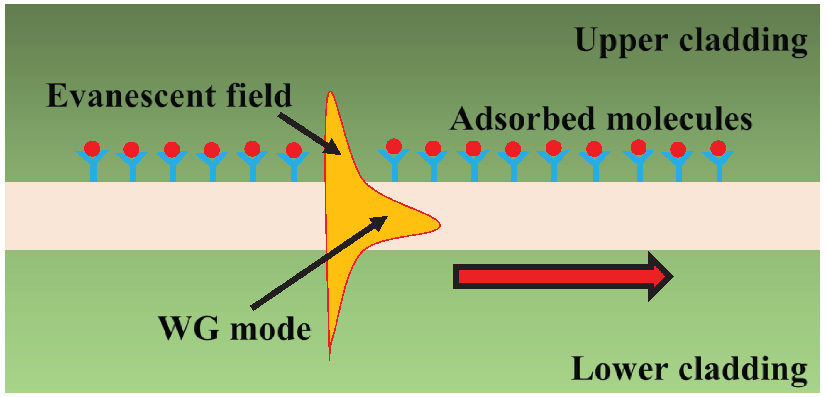
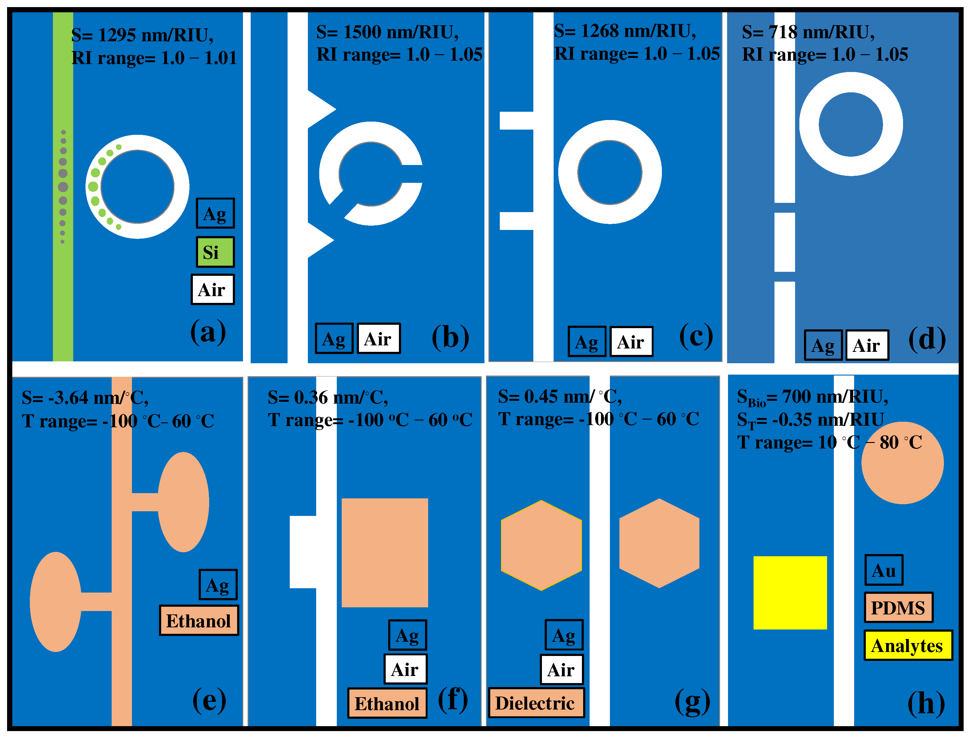
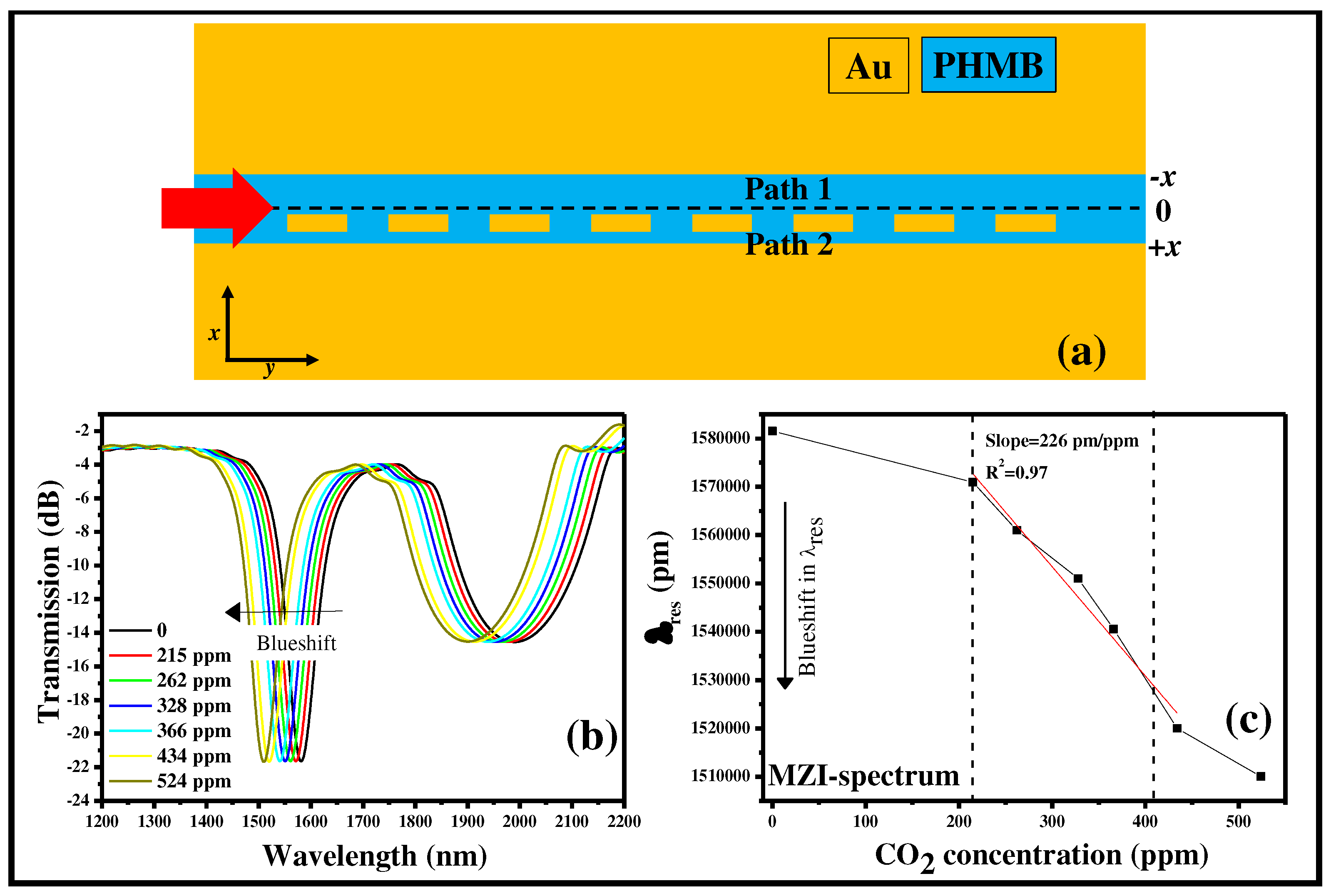
| Device Type | Experiment/ Simulation |
Sensitivity | FOM | Q-factor | LOD | Ref. |
|---|---|---|---|---|---|---|
| RR established on ridge W/G | Experiment | 112 nm/RIU | - | - | 1.6x10⁻⁶ | [51] |
| PC heterostructure cavities | Experiment | 1500 nm/RIU | - | 50000 | 7.8x10⁻⁶ | [52] |
| RR established on ridge W/G | Experiment | 2169 nm/RIU | - | - | 8.3x10⁻⁶ | [53] |
| 2D PC microcavity | Experiment | 200 nm/RIU | - | 400 | 0.002 | [54] |
| RR established on ridge W/G | Simulation | 167 nm/RIU | 49.9 | 561.6 | 2.75x10⁻² | [55] |
| PC slot microcavity | Experiment | 370 nm/RIU | - | 7500 | 2.3x10⁻⁵ | [56] |
| RR established on slot W/G | Experiment | - | - | - | 5x10⁻⁶ | [57] |
| RR established on slot W/G | Experiment | 298 nm/RIU | - | - | 4.2x10⁻⁵ | [58] |
| Mach Zehnder Interferometer | Experiment | 2.5 pm/K | - | - | - | [59] |
| RR established on SWG double slot W/G | Simulation | 840 nm/RIU | 6461.5 | 9246.2 | - | [2] |
| Grating sensor | Experiment | 1606.2 nm/RIU | - | - | 3x10⁻⁵ | [60] |
| PC point defect resonant cavity | Simulation | 330 nm/RIU | - | 3820 | 0.001 | [61] |
| Young Interferometer | Experiment | 2.2 rad/oC | - | - | 6.4x10⁻⁶ | [62] |
| PC ring-slot structure | Simulation | 160 nm/RIU | - | 107 | 8.75x10⁻⁵ | [63] |
| RR established on SWG hybrid plasmonic W/G | Simulation | 1000 nm/RIU | 287.35 | 441.05 | - | [64] |
| Young Interferometer | Experiment | 0.051 | - | - | 1x10⁻⁶ | [65] |
| RR coupled phase-shifted BG resonator | Simulation | 297.13 nm/RIU | - | 2000 | 1.1x10⁻⁴ | [50] |
| Slot RR and BG | Simulation | 211.43 nm/RIU | - | 1720 | 1.26x10⁻³ | [66] |
| RR established on SWG | Simulation | 7061 nm/RIU | - | 15918 | 1.74x10⁻⁵ | [48] |
| Ref. | Fiber Type | Application | Sensitivity | Sensing Mechanism | Year |
|---|---|---|---|---|---|
| [112] | U-shaped MMF | Biosensing | 1251.44 nm/RIU | LSPR | 2020 |
| [113] | Plastic OF | Cholesterol detection | 140 mg/dL to 250 nm/dL | - | 2017 |
| [114] | SMF | Temperature | 210.25 KHz/oC | Vernier effect | 2020 |
| [115] | Fiber tip integrated ZnO-nanowire-nanograting | Temperature | 0.066 nW/oC | Bragg reflection | 2023 |
| [116] | Magnetic field micro-nano fiber | Magnetic field | 69 pm/Gs | Mach-Zehnder interference | 2022 |
| [117] | PC fiber | Biosensing | 12000 nm/RIU and 16000 nm/RIU | SPR | 2020 |
| [118] | D-shaped OF | Biosensing | 5161 nm/RIU | SPR | 2018 |
| [119] | D-shaped OF | Biosensing | 4122 nm/RIU | LMR | 2018 |
| [120] | PC fiber | Temperature | 0.1636 nm/oC | Quantum dot | 2009 |
| [121] | D-shaped PC fiber | Biosensing | 20000 nm/RIU | SPR | |
| [122] | D-shaped PC fiber | Biosensing | 21700 nm/RIU | SPR | 2017 |
| [123] | Octagonal PC fiber | Transformer oil | 31240 RIU-1 (x-pol.), 30830 RIU-1 (y-pol.) |
Plasmonic | 2020 |
| [124] | Elliptical channel PC fiber | Malaria detection | 11428.57 nm/RIU, 9473.68 nm/RIU, 9655.17 nm/RIU | - | 2021 |
| Polarization | RI Range | S (nm/RIU) | Reference |
|---|---|---|---|
| (I) x-polarized mode (II) y-polarized mode |
- | 4156.82 (I) 3703.64 (II) |
[143] |
| y-polarized mode | 1.36-1.40 | 33500 | [144] |
| (I) x-polarized mode (II) y-polarized mode |
1.33-1.45 | 10448.5 (I) 8230.07 (II) |
[145] |
| (I) x-polarized mode (II) y-polarized mode |
1.330-1.370 | 5000 (I) 10000 (II) |
[146] |
| (I) x-polarized mode (II) y-polarized mode |
1.33-1.40 | 9000 (I) 9000 (II) |
[147] |
| x-polarized mode | 1.0-1.05 | 508 | [148] |
| x-polarized mode | - | 510 | [139] |
| y-polarized mode | 1.0-1.0010 | 3200 | [140] |
| y-polarized mode | 1.33-1.43 | 2150 | [149] |
| y-polarized mode | 1.33-1.37 | 1000 | [150] |
| y-polarized mode | 1.4-1.44 | 9180 | [151] |
| (I) x-polarized mode (II) y-polarized mode |
1.33-1.34 | 2000 (I) 1700 (II) |
[152] |
| x-polarized mode | 1.0-1.377 | 160 | [63] |
| x-polarized mode | 1.0-2.0 | 65.7 | [153] |
| y-polarized mode | 1.0-1.8 | 396 | [154] |
| y-polarized mode | 1.0-1.33 | 300 | [155] |
| Ref. | Device Design | Material | Wavelength Range | Application | Sensitivity |
|---|---|---|---|---|---|
| [173] | Square and hollow square meta-atoms | Si-dielectric-metal | NIR | Temperature Biosensing |
-0.18 nm/oC 355 nm/RIU |
| [175] | Nano-trench | Graphene | NIR | Biosensing | 500 nm/RIU to 1000 nm/RIU |
| [176] | Rectangular strip | Dielectric-metal | MIR | Biosensing | 1800 nm/RIU |
| [177] | Square | Si-dielectric-metal | NIR | Biosensing | 460 nm/RIU to 492 nm/RIU |
| [178] | Square | Metal-dielectric | NIR | Biosensing | 840 nm/RIU |
| [179] | Cylinder | InSb | THz | Biosensing | 1800 GHz/RIU to 1900 GHz/RIU |
| [180] | Cylinder | Metal-dielectric-metal | NIR | Biosensing | 1109 nm/RIU to 1290 nm/RIU |
| [181] | C-shape split ring | GST phase changing material | NIR | Biosensing | 1000 nm/RIU |
| [182] | Metal disc | Metal-graphene | FIR | Biosensing | 3.98 μm/RIU to 5.06 μm/RIU |
| [169] | Cylinder | Si-dielectric-metal | NIR | Gas | 17.3 pm/ppm |
| [183] | Vertical strip-ring | Metal | THz | Biosensing | 908 nm/RIU to 4367 nm/RIU |
| [184] | - | Gold-Si-Graphene | THz | Biosensing | 66 GHz/RIU |
| [185] | Cross array | Si-gold | THz | Biosensing | 25.3 THz/RIU to 41.3 THz/RIU |
| Ref. | Application | Sensitivity | FOM | Q-Factor | Year |
|---|---|---|---|---|---|
| [221] | (I) Gas, (II) biochemical |
(I) 3639.79 nm/RIU, (II) 7530.49 nm/RIU |
91.02 | 99.75 | 2022 |
| [220] | Gas | 226 pm/ppm | 0.004 | 24.7 | 2022 |
| [222] | Bio-analytes | 3000 nm/RIU | 9.7 x10⁵ | - | 2022 |
| [215] | Bio-analytes Temperature |
700 nm/RIU, -0.35 nm/oC |
21.9, 0.008 |
- | 2021 |
| [223] | Bio-analytes Temperature |
-0.58 nm/oC and -0.64 nm/oC 1240 nm/RIU and 1350 nm/RIU |
(I) 8.6 and 1955.2, (II) 18.74 and 691 |
- | 2022 |
| [224] | Bio-analytes | 1578 nm/RIU | 175 | - | 2022 |
| [225] | Temperature, Glucose |
1.55 nm/oC, 4074 nm/RIU |
2.45x10⁻⁶ | - | 2022 |
| [226] | Bio-analytes | 825.7 nm/RIU | 13.14 | - | 2022 |
| [227] | Bio-analytes | 7872 nm/RIU | 394 | - | 2022 |
| [228] | Pressure | 10.96 and 10.5 nm/MPa | - | - | 2022 |
| [229] | Bio-analtyes | 2473 nm/RIU | 34.18 | 56.35 | 2021 |
| [230] | Pressure | 25.4 nm/MPa | - | - | 2021 |
| [231] | Pressure | 16.5 nm/MPa | - | - | 2018 |
| [232] | Bio-analytes | 1948.67 nm/RIU | 29.52 | 29.90 | 2020 |
| [233] | Bio-analytes | 2300 nm/RIU | 31.5 | 31.1 | 2020 |
| [205] | Gas | 135.95 pm/ppm | - | - | 2021 |
| [234] | Bio-analytes | 793.3 nm/RIU | 52.9 | 82.1 | 2019 |
| [235] | Bio-analytes Temperature |
1406.25 nm/RIU 0.45 nm/oC |
156.25 | - | 2021 |
| [236] | Temperature Glucose |
1.525 nm/oC 0.45 nm.L/g |
52.73 | - | 2021 |
Disclaimer/Publisher’s Note: The statements, opinions and data contained in all publications are solely those of the individual author(s) and contributor(s) and not of MDPI and/or the editor(s). MDPI and/or the editor(s) disclaim responsibility for any injury to people or property resulting from any ideas, methods, instructions or products referred to in the content. |
© 2023 by the authors. Licensee MDPI, Basel, Switzerland. This article is an open access article distributed under the terms and conditions of the Creative Commons Attribution (CC BY) license (http://creativecommons.org/licenses/by/4.0/).

