1. Introduction
Metal oxides are widely studied with respect to their electrochromic behavior and properties for the applications as display devices and smart windows. To decrease the absorbed heat in buildings, electrochromic films have been used as smart windows for preservation the glass windows from the extra heating [
1]. Electrochromic materials have been applied in energy-effective vitrification, automobile sunroofs, smart windows, and mirrors. Transition metal oxides such as titanium, tungsten, nickel, vanadium, and molybdenum oxides have been considered the most promising electrochromic materials [
2]. The formation of smart window contains a layer of electrochromic material bounded by metal oxide layers. To turn transparent glass opaque and back to the transparent state, low electric current is used. The transmittance can be controlled by modifying the optical properties.
The protection from heat radiation through glass is made by semiconductor metal oxide film coatings on glass, such as TiO
2, WO
3, CrO, NiO, Nb
2O
5, and IrO
2 [
3], MoO
3 [
4,
5].
Typically, nanoscale oxides are considered according to their high thermal conductivity, low thermal expansion coefficient and the insulation. Application of this type of coating gives advanced surface quality. The heat transfer rate and the thermal conductivity have been increased due to the increases in concentration of nano particles. [
6,
7].
Several methods of deposition can be considered: sputtering [
8], sol-gel method [
4], sintering [
9], Atmospheric Pressure Chemical Vapor Deposition (APCVD) [
10], and dipping [
11].
The colored state of pure TiO
2 coatings is gray and this oxide was not used alone in electrochromic devices because its coloration is not very strong [
3]. Titanium oxide films have been sputter-deposited in a non-aqueous medium, spray deposited from reactive sputtering. Chronoamperometric experiments associated with transmittance spectra in LiClO
4-propylene carbonate solutions were carried out and compared with the optical properties of titanium oxide films with different stoichiometries. [
12].
Spectroscopic Ellipsometry (SE) is a high accuracy optical characterization technique [
13]. Many researchers have used SE for pure or combinatorial material investigation [
14,
15,
16,
17,
18,
19,
20,
21].
Combinatorial approach to investigate mixed metal oxides has several advantages. Fried et al. [
22] have used SE (which is fast, cost-effective, and non-destructive method) for investigation and mapping WO
3-MoO
3 mixed layers after sputtering. Different optical models (such as Effective Medium Approximation (EMA) and oscillator-type ones) have been used to achieve the composition map and thickness map of the sample layers.
While TiO
2 was investigated as electrochromic material [
23], SnO
2 or TiO
2-SnO
2 [
24,
25] mixtures were studied only as photocatalytic materials. During this work, reactive magnetron sputtering (in Ar-O
2 plasma) has been used to produce all combinations of TiO
2-SnO
2 mixed layers on silicon wafers. The sample preparation time took 4 hours in the vacuum chamber including the vacuum-preparation time. By using the combinatorial process, all the compositions have been achieved in the same sputtering chamber after one sputtering. Scanning Electron Microscopy (SEM) with Energy-Dispersive X-ray Spectroscopy (EDS) has been used to check the SE results.
The object of this work was to investigate the goodness of TiO2-SnO2 mixed layers as electrochromic materials, and to contrast the 'goodness' of the diverse optical models, and to enhance the electrochromic properties demeanor of mixed metal oxides that were deposited by reactive sputtering. We expected that using different diameter metal atoms in the layer will have a positive effect.
2. Materials and Methods
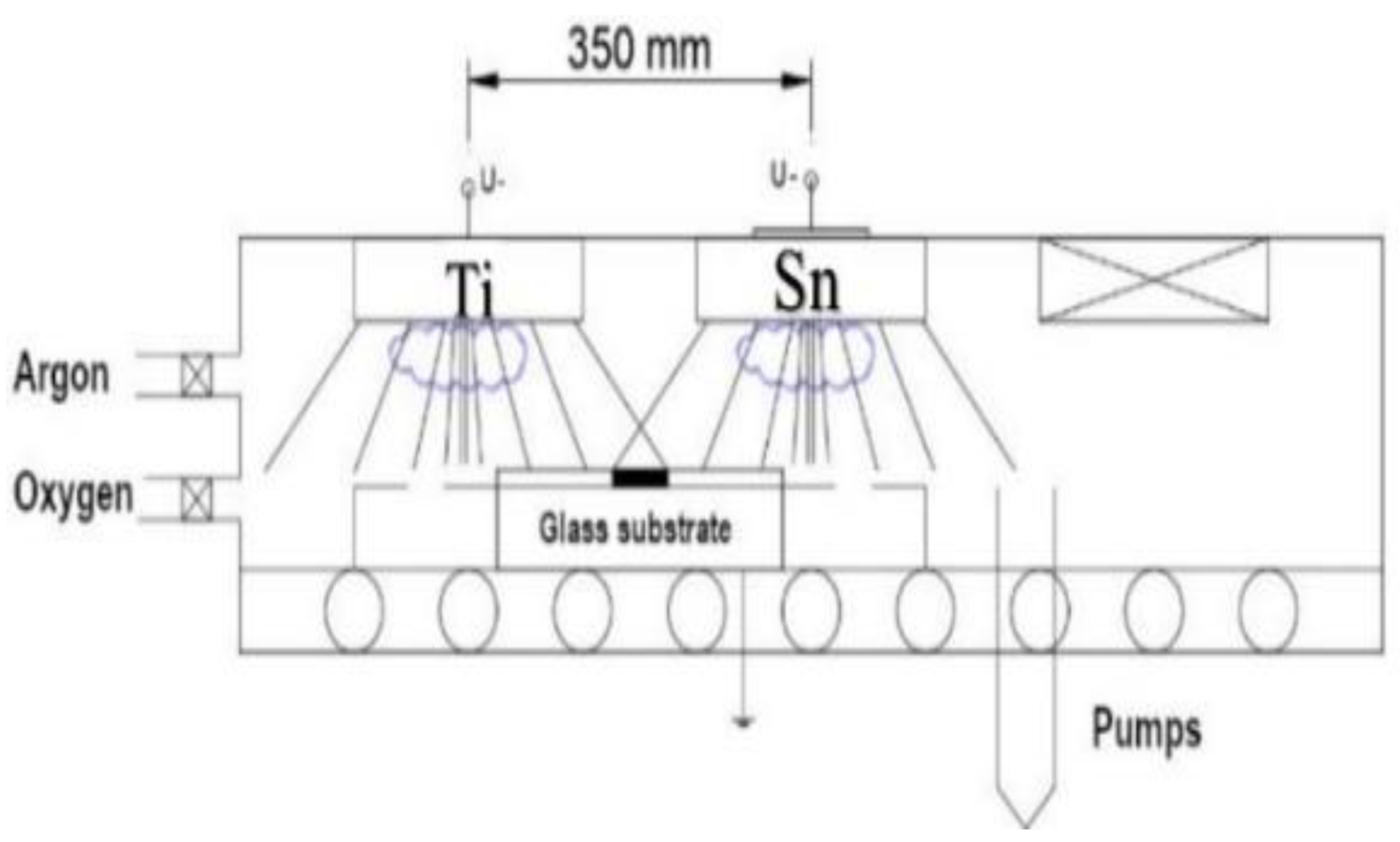
In the chamber of magnetron sputtering, the layers were deposited in a reactive (Ar + O2) gas mixture in ~2 × 10⁻⁶ mbar high vacuum, was the pressure of the process was ~10−3 mbar. 30 sccm/s Ar and 30 sccm/s O2 volumetric flow rate has been applied inside the chamber. The substrates were 4-inch diameter IC-grade and 3-inch diameter highly conductive (0.001 Ωcm) Si-wafers.
The movement speed was 5 cm/s (back and forth) in the geometry which can be seen in
Figure 1. 50-50 % composition can be expected in the middle of the specimen. The Si-wafers and control Si-stripes were placed on a 30 cm × 30 cm glass, see Fig.1. The power of the plasma was in the range of 0.75–1.5 kW for the two targets, and independently controlled. 300 walking cycles were applied with 5 cm/s movement speed.
Figure 1 presents that sputtering targets have been placed at 35 cm from each other. According to the measurements, the two sputtered material fluxes ‘material streams’ are overlapped around the center. The Metal/Oxygen atomic ratio in the layers was 1:2 at the applied Oxygen partial pressure according to the SEM-EDS analysis technique.
The optical mapping [
21] was performed by a Woollam M2000 SE equipment, the measurements were evaluated with the CompleteEASE software [
26]. To obtain the mapping parameters, oscillator functions and compact optical models have been used. The „goodness” of the optical model depends on the value of the Mean Squared Error (MSE), so the lower MSE refers to the better fit because of the difference between curves. [
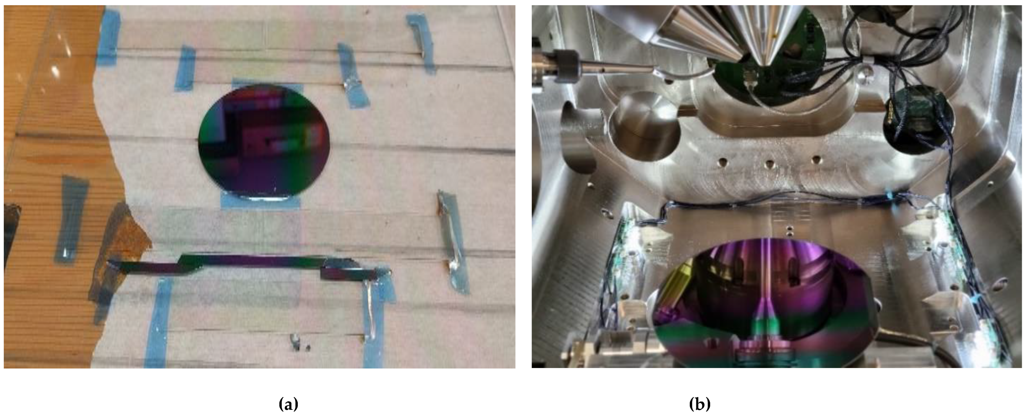
13] The silicon wafers and Si-stripes (
Figure 2a have been used for Scanning Electron Microscopy (SEM, Dual-beam SEM+FIB Thermo Scientific Scios2) with Energy Dispersive Spectroscopy (EDS) measurements, too, see
Figure 2b. The Ti/Sn ratio has been calculated point-by-point to compare and validate the results of the SE evaluation.
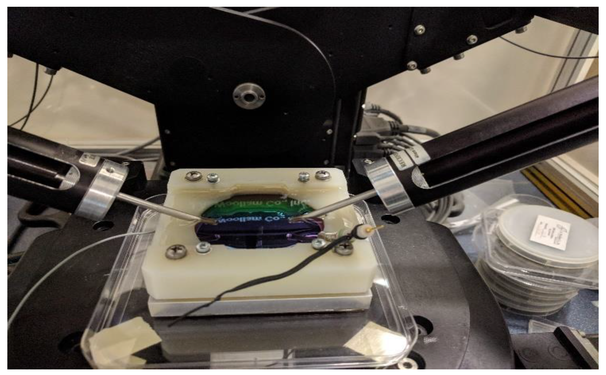
The coloration process was followed point by point of the layer deposited onto the 3-inch diameter highly conductive (0.001 Ωcm) Si-wafer. Electrochemical measurements were performed in a liquid cell filled with 1M lithium perchlorate (LiClO
4) / propylene carbonate electrolyte, and a Pt wire counter electrode was placed into the electrolyte alongside with a reference electrode, see
Figure 3. Controlled current was applied through the cell during a 4 min coloration.
After the coloration process, the whole sample (in dry state) was mapped by SE. The edges were under the Teflon cover (during the coloration process) so only the central 4 cm diameter part is interesting, see
Figure 3.
3. Results
We compared two dispersion relations in our multilayer optical model (Si-substrate/interface-layer/T-L(TiO
2)+T-L(SnO
2)-mixed layer/surface-roughness-layer). In the Bruggeman Effective Medium Approximation (EMA or BEMA [
27]) calculation, the mixed-layer is considered as a physical combination of two distinct phases formed by TiO
2 and SnO
2 with an appropriate volume fraction. The constituents are considered equivalent; neither of the components is considered as a host material.The formula as in equations (1):
where ε is the effective complex dielectric function of the composite layer; f
i and ε
i denote volume fraction and the complex dielectric function of the ith component. In the case of two components, the formula is a complex quadratic equation, where ε (the effective dielectric function) is the unknown and we can choose easily between the two solutions (the wrong one is physically meaningless). The dielectric function of the two constituents were determined from the extreme edges of the Si-stripes where the TiO
2 and SnO
2 are in pure format.
The Tauc-Lorentz (T-L) oscillator model is a combination of the Tauc and Lorentz models [
28]. Tauc-Lorentz (T-L) oscillator model contains four parameters: Transition Amplitude, Broadening coefficient of the Lorentz oscillator, peak position for the Lorentz oscillator, and Bandgap Energy (E
g), which is taken to be the photon energy, where ε
2 (E) reaches zero. When the E photon energy is less than the bandgap energy, E
g, ε
2 (E) is zero. The real part of the dielectric function ε
1 (E) can be obtained from ε
2 (E) through the Kramers-Kronig relation.
In the mixed layers, five fitting parameters have been used: two Amplitudes for each materials (oscillator strengths) and the layer thickness. We used the measurements near the edges of the samples (pure component materials) to determine the fundamental parameters (Bandgap Energies, the Broadenings and the Peak positions) for the two materials.
For the electrochromic measurements, where the light absorption was interesting in the visible wavelength region over 400 nm, we used the simple Cauchy formula to describe the complex refractive as in formula: N = n + ik, where N is the complex refractive index, n is the real part of N, k is the imaginary part (extinction), i is the imaginary unit. Cauchy formula: n(λ) = A+B/λ2+C/λ4, k(λ) = ke U( 1239.84/λ − Eb), where A, B, C, k, and U are fitting parameters. The complex refractive index (N) and complex dielectric function (ε) are equivalents: (ε) = ε1+iε2 = N2, ε1 = n2−k2, ε2 = 2nk.
3.1. Comparison of the optical models
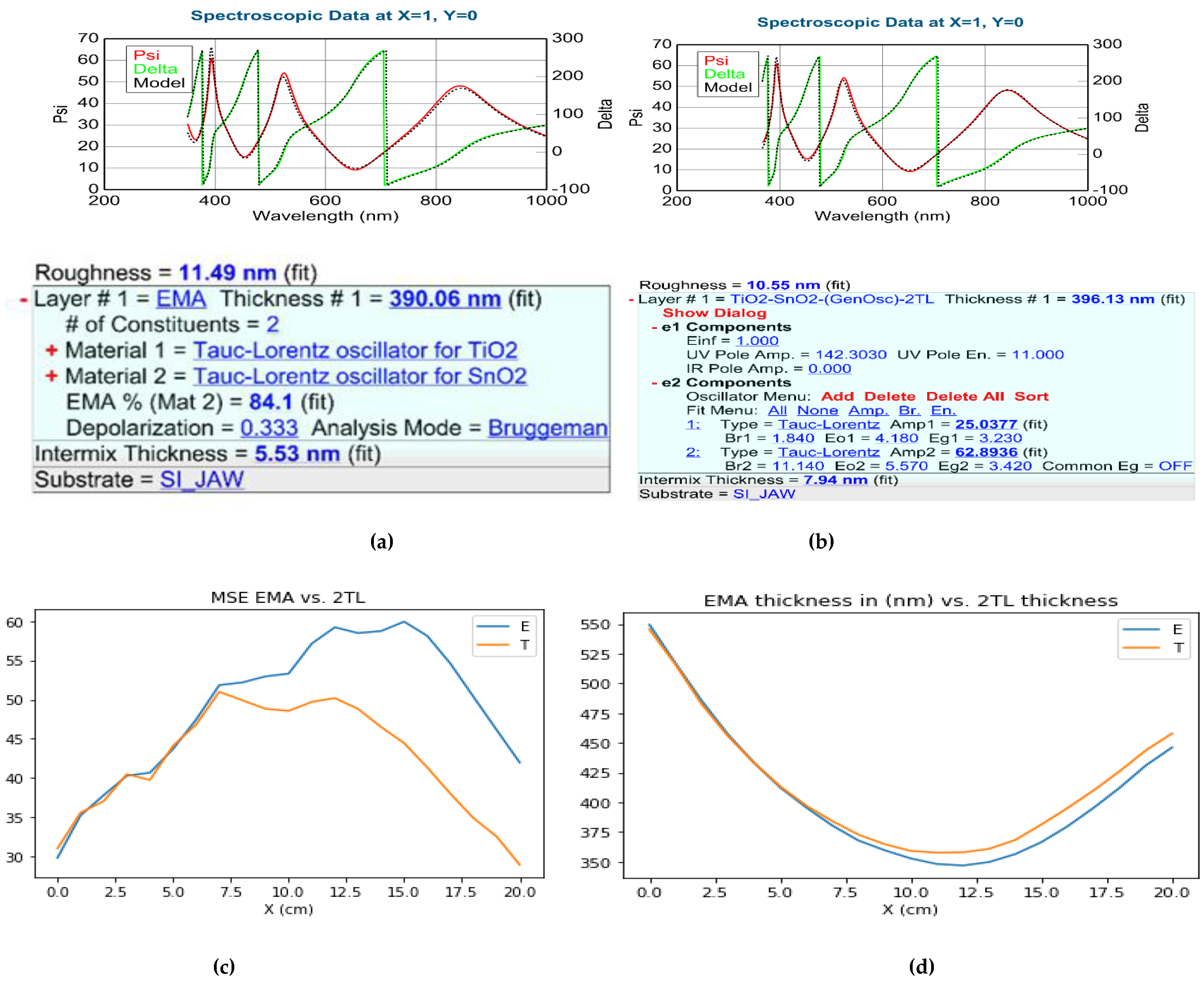
We applied the 2-T-L and the EMA optical model to evaluate the mapping measurements on the Si-stripes (see
Figure 4) and the 4-inch Si-wafer (see
Figure 5). Both modelling process gave good results, see
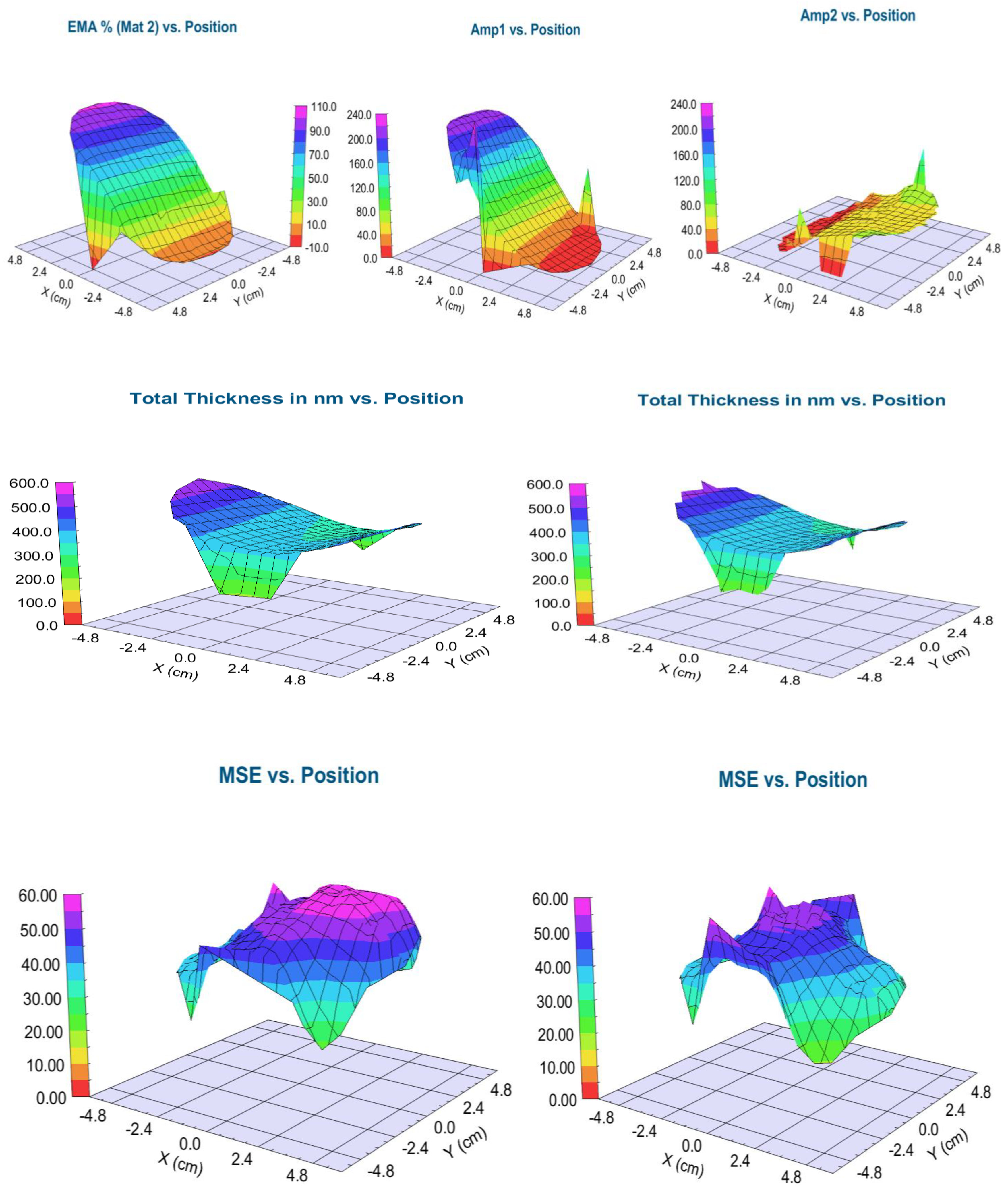
Figure 4 where the measured Psi and Delta spectra are in good agreement with the Model calculations. However, one can see that the MSE (Mean Squared Error) is significantly lower for the 2-T-L model especially around the 50-50 % composition, see
Figure 4c and
Figure 5 lower row. The calculated thickness values are not different significantly, see
Figure 4d and
Figure 5 middle row.
4. Discussion
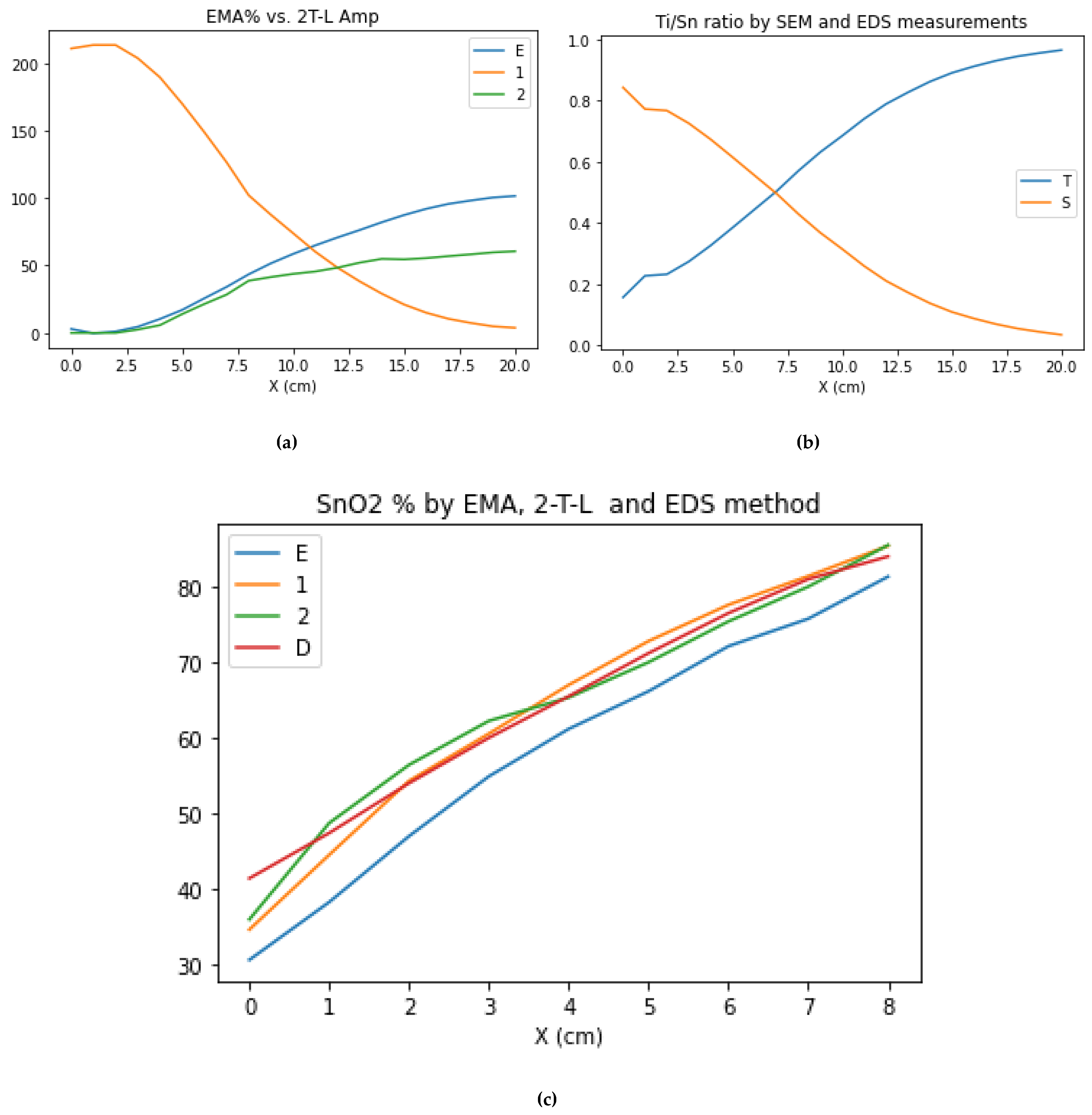
We validated the results of the SE modeling by SEM-EDS measurements, see
Figure 6b.
Figure 6a shows the EMA % (MAT2 - SnO
2 %) values from the EMA model and the Amp1 (TiO
2 oscillator strength) and the Amp2 (SnO
2 oscillator strength) from the 2-Tauc-Lorentz (2-T-L) model.
Figure 6c shows the results together, where we normalized the Amp1 and Amp2 to 100 %. One can see the good agreement between the SEM-EDS and the 2-T-L results.
4.1. Electrochromic measurements
After the validation of the SE method (we can determine the composition of the layer) we performed in-situ electrochromic measurement, see
Figure 3. We could measure only at the central point of the highly conductive 3-inch Si-wafer.
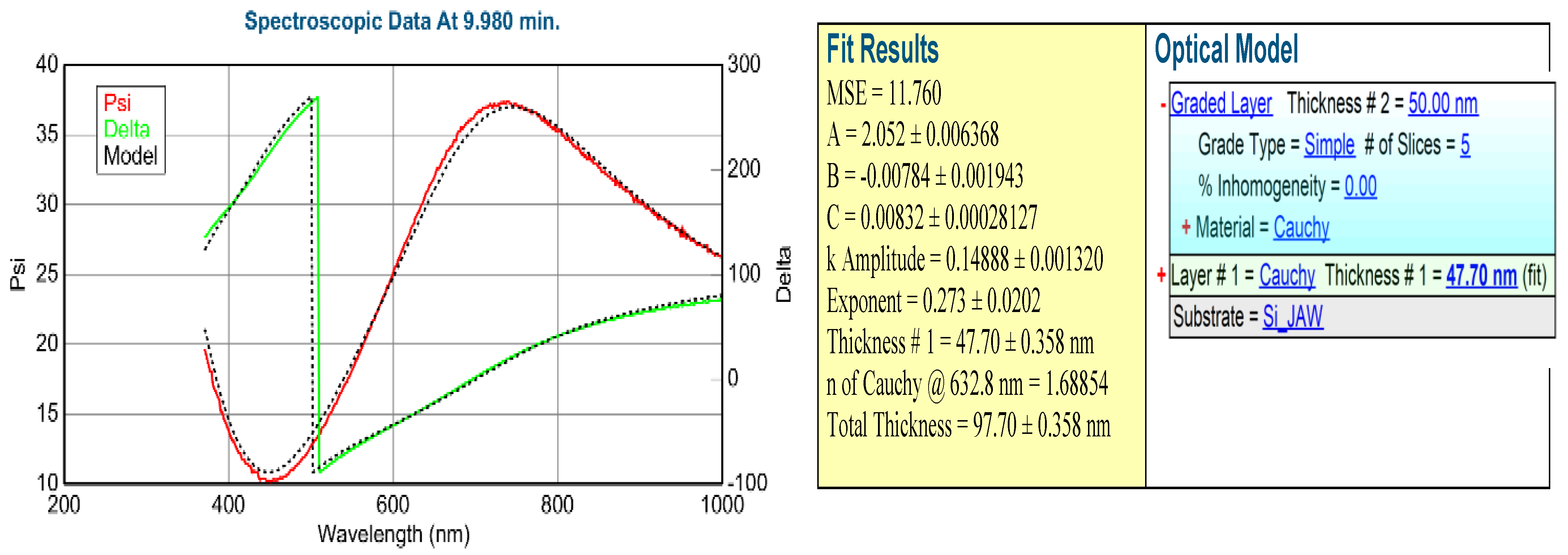
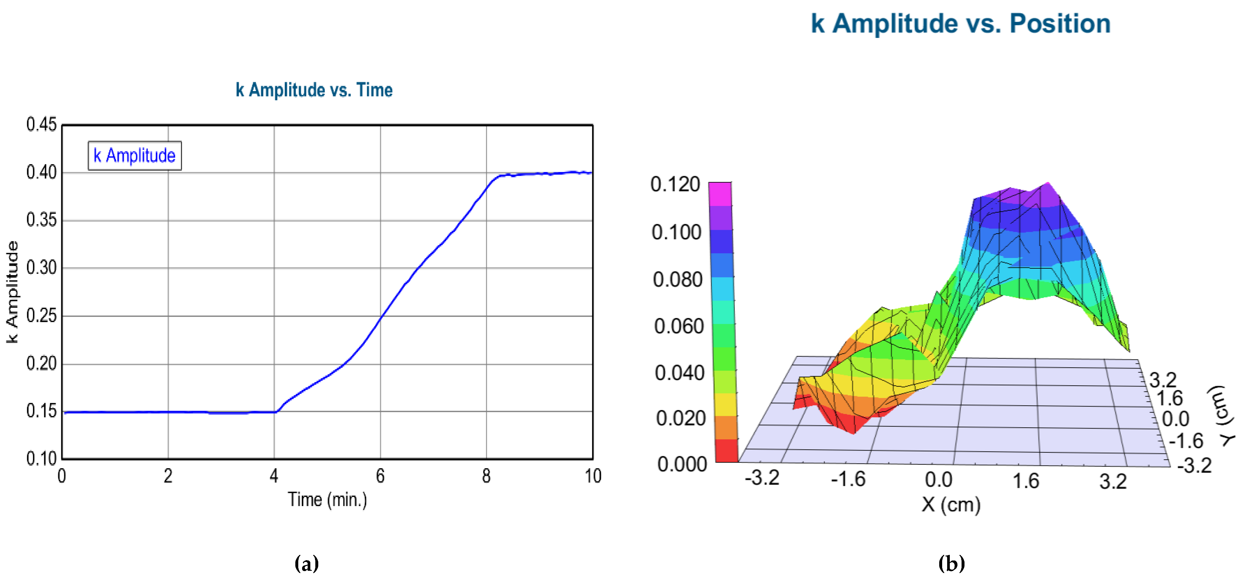
Figure 7 show a typical example of one measured spectra pair with the Model calculation based on the Optical model shown on the right side. Low MSE value shows that the optical model is good. We could follow the process, calculating the change of the k parameter, see
Figure 8a.
After the coloration process, we could map the colorized layer using a simple one-layer Cauchy dispersion optical model. (Note, that this is not the same model as it was used in the in-situ measurement!) We see a maximum value (maximum light absorption) around 0.5 cm. Comparing this results with
Figure 6, we can state that the optimal composition is at TiO
2 0,3-SnO
2 0,7.
5. Conclusions
We could optimize the electrochromic properties of mixed metal oxides deposited by reactive sputtering. We prepared combinatorial samples by magnetron sputtering. These samples have been mapped (composition and thickness maps) by Spectroscopic Ellipsometry which is a fast, cost-effective, and non-destructive method. We can select between suitable optical models (the Bruggeman Effective Medium Approximation, BEMA vs. 2-Tauc-Lorentz oscillator model) according upon the process parameters. We have shown that in case of molecular-level mixed layers 2-Tauc-Lorentz oscillator model is better than the Bruggeman Effective Medium Approximation. We have shown that the optimal composition is at. TiO2 0,3-SnO2 0,7.
Acknowledgments
This research was funded by NKFIH OTKA NN 131269 (VOC-DETECT M-ERA.NET Transnational Call 2018) and NKFIH OTKA K 128319 and 131515 projects. Project TKP2021-EGA-04 has been implemented with the support provided by the Ministry of Innovation and Technology of Hungary from the National Research, Development, and Innovation Fund, financed under the TKP2021 funding scheme. The work in frame of the 20FUN02 ‘‘POLight’’ project has received funding from the EMPIR programme co-financed by the Participating States and from the European Union’s Horizon 2020 research and innovation programme. Noor Taha Ismaeel is grateful for the Stipendium Hungaricum scholarship.
References
- Granqvist, C.G. Handbook of Inorganic Electrochromic Materials. Elsevier, Amsterdam, The Netherlands 1995.
- Yingxi Lu; Liang Liu; Daniel Mandlerb and Pooi See Lee. High switching speed and coloration efficiency of titanium-doped vanadium oxide thin film electrochromic devices. Journal of Materials Chemistry C. October 2013. [CrossRef]
- Livage, J.; Ganguli, D. Sol-gel electrochromic coatings and devices. A review. Sol. Energy Mater. Sol. Cells 2001, pp. 365–381.
- Lin, S.-Y.; Wang, C.-M.; Kao, K.-S.; Chen, Y.-C.; Liu, C.-C. Electrochromic properties of MoO3 thin films derived by a sol–gel process. J. Sol Gel Sci. Technol 2010, pp. 53, 51–58.
- Hsu, C.S.; Chan, C.C.; Huang, H.T.; Peng, C.H.; Hsu, W.C. Electrochromic properties of nanocrystalline MoO3 thin films. Thin Solid Film 2008, pp. 516, 4839–4844. [CrossRef]
- M. I. Kandil; H. S. Jahin; et al. Synthesis and characterization of γ- Al2O3 and α-Al2O3 nanoparticles using a facile, inexpensive autocombustion approach. Egypt. J. Chem. 2021, Volume 64, No.5, pp. 2509 – 2515.
- Kusammanavar Basavaraj; Dr. K Elangovan; Dr. Suneelkumar N Kulkarni; Dr. Shankar S. Effect of Concentration of Al2O3 Nano Particles in Base Fluid on Thermal and Flow Properties to Enhance the Heat Transfer Rate. INTERNATIONAL JOURNAL OF ENGINEERING RESEARCH & TECHNOLOGY (IJERT) 2021, Volume 10, Issue 02.
- Madhavi, V.; Jeevan Kumar, P.; Kondaiah, P.; Hussain, O.M.; Uthanna, S. Effect of molybdenum doping on the electrochromic properties of tungsten oxide thin films by RF magnetron sputtering. Ionics 2014, pp. 20, 1737–1745. [CrossRef]
- Prameelaand, C.; Srinivasarao, K. Characterization of (MoO3)x-(Wo3)1-x composites. International Journal of Applied Engineering Research 2015, pp.10, 9865–9875.
- Ivanova, T.; Gesheva, K.A.; Kalitzova, M.; Hamelmann, F.; Luekermann, F.; Heinzmann, U. Electrochromic mixed films based on WO3 and MoO3 obtained by an APCVD method. J. Optoelectron. Adv. Mater 2009, pp. 11, 1513–1516.
- Novinrooz, A.; Sharbatdaran, M.; Noorkojouri, H. Structural and optical properties of WO3 electrochromic layers prepared by the sol-gel method. Cent. Eur. Sci. J. 2005, pp. 3, 456–466. [CrossRef]
- M.P. Cant; J.I. Cisnero; R.M. Torresib. Electrochromic behavior of sputtered titanium oxide thin films. ELSEVIER, Thin Solid Films 1995, pp. 259, 70-74.
- Hiroyuki Fujiwara. Spectroscopic Ellipsometry Principles and Applications, Publisher: John Wiley & Sons, 2007; ISBN: 0470060182, 9780470060186.
- Zimmer, A.; Gilliot, M.; Broch, L.; Boulanger, C.; Stein, N.; Horwat, D. Morphological and chemical dynamics upon electrochemical cyclic sodiation of electrochromic tungsten oxide coatings extracted by in situ ellipsometry. Appl. Opt. 2020, pp. 59,3766–3772. [CrossRef]
- Hales, J.S.; DeVries, M.; Dworak, B.; Woollam, J.A. Visible and infrared optical constants of electrochromic materials for emissivity modulation applications. Thin Solid Film 1998, pp.313–314, 205. [CrossRef]
- Sauvet, K.; Rougier, A.; Sauques, L. Electrochromic WO3 thin films active in the IR region. Sol. Energy Mater. Sol. Cells 2008, pp. 92, 209–215. [CrossRef]
- Shan, A.; Fried, M.; Juhasz, G.; Major, C.; Polgár, O.; Németh, Á.; Petrik, P.; Dahal, L.R.; Chen, J.; Huang, Z. High-speed imaging/mapping spectroscopic ellipsometry for in-line analysis of roll-to-roll thin-film photovoltaics. IEEE J. Photovolt 2014, pp. 4, 355–361. [CrossRef]
- Koirala, P.; Tan, X.; Li, J.; Podraza, N.J.; Marsillac, S.; Rockett, A.; Collins, R.W. Mapping spectroscopic ellipsometry of CdTe solar cells for property-performance correlations. In Proceedings of the 2014 IEEE 40th Photovoltaic Specialist Conference (PVSC), Denver, CO, USA, pp. 0674–0679, 8–13 June (2014).
- Dahal, L.R.; Li, J.; Stoke, J.A.; Huang, Z.; Shan, A.; Ferlauto, A.S.; Wronski, C.R.; Collins, R.W.; Podraza, N.J. Applications of real-time and mapping spectroscopic ellipsometry for process development and optimization in hydrogenated silicon thin-film photovoltaics technology. Sol. Energy Mater. Sol. Cells 2014, pp. 129, 32–56. [CrossRef]
- Aryal, P.; Pradhan, P.; Attygalle, D.; Ibdah, A.-R.; Aryal, K.; Ranjan, V.; Marsillac, S.; Podraza, N.J.; Collins, R.W. Real-time, in-line, and mapping spectroscopic ellipsometry for applications in Cu (in Ga) Se metrology. IEEE J. Photovolt 2014, pp. 4, 333–339.
- Peter Petrik; Miklos Fried. Mapping and Imaging of Thin Films on Large Surfaces. A review. physica status solidi (a) 2022, Volume 219, 2100800. Published by Wiley-VCH GmbH381. [CrossRef]
- Fried, M.; Bogar, R.; Takacs, D.; Labadi, Z.; Horvath, Z.E.; Zolnai, Z. Investigation of Combinatorial WO3-MoO3 Mixed Layers by Spectroscopic Ellipsometry Using Different Optical Models. Nanomaterials 2022, pp. 12, 2421. [CrossRef]
- Erbil Şilik; Suat Pat; Soner Özen; Reza Mohammadigharehbagh; H. Hakan Yudar; Caner Musaoğlu; Şadan Korkmaz. Electrochromic properties of TiO2 thin films grown by thermionic vacuum arc method. Thin Solid Films 2017, Volume 640, pp. 27-32. [CrossRef]
- Shankar Sharma; Naveen Kumar; Peter R. Makgwane; Nar Singh Chauhan; Kavitha Kumari; Manju Rani; Sanjeev Maken. TiO2/SnO2 nano-composite: New insights in synthetic, structural, optical and photocatalytic aspects, Inorganica Chimica Acta 2022, Volume 529, 120640. [CrossRef]
- Rekha B. Rajput; Shweta N. Jamble; Rohidas B. Kale. A review on TiO2/SnO2 heterostructures as a photocatalyst for the degradation of dyes and organic pollutants. Journal of Environmental Management 2022, Volume 307, 114533. [CrossRef]
- Available online: https://www.jawoollam.com/products/m-2000-ellipsometer (accessed on 2022-07-12).
- Bruggeman, D.A.G. Dielectric constant and conductivity of mixtures of isotropic materials. Ann. Phys. 1935, Volume 24, pp. 636–664. [CrossRef]
- Jellison, G.E., Jr.; Modine, F.A. Parameterization of the optical functions of amorphous materials in the inter band region. Appl. Phys. Lett. 1996, Volume 69, pp. 371–373.
|
Disclaimer/Publisher’s Note: The statements, opinions and data contained in all publications are solely those of the individual author(s) and contributor(s) and not of MDPI and/or the editor(s). MDPI and/or the editor(s) disclaim responsibility for any injury to people or property resulting from any ideas, methods, instructions or products referred to in the content. |
© 2023 by the authors. Licensee MDPI, Basel, Switzerland. This article is an open access article distributed under the terms and conditions of the Creative Commons Attribution (CC BY) license (http://creativecommons.org/licenses/by/4.0/).
