1. Introduction
Transition-metal nitride thin-film materials, such as copper nitride (
), exhibit very attractive and remarkable physical properties, such as optical, electrical and energy-storage properties, which have enable to this particular material to be employed in many technological-application fields [
1,
2]. Consequently, copper nitride has drawn great deal of attention as a new
eco-friendly solar-absorber material, for flexible and lightweight thin-film photovoltaic cells [
3,
4]. This metastable semiconductor material is
non-toxic, made up of earth-abundant elements, and its band-gap energy can be relatively easily tunable, depending upon both the manufacturing conditions, and the deposition techniques. Among the fields of applications, it can be indicated the following: integrated circuits, photo-detectors, optoelectronics, and energy-conversion applications [
5,
6,
7]. Emphasizing again the mentioned specific use of
as a novel
solar absorber thin-layer material for photovoltaic-cell technology [
8]: Its development has caused a notable interest with the goal of being introduced into novel designs, within a future generation of cost-effective solar cells. This recently-gained attention as a
light absorber in solar-cell, is mainly based upon its mentioned clear non-toxicity and significant earth abundance, which produces such an environmentally friendly material. Furthermore, the theoretically-predicted band-gap value for
is approximately
[
9,
10], but its experimentally-obtained values of the indirect and direct band gaps are found to be within the energy ranges from
up to
, and from
up to
, respectively [
10,
11]. These obtained values imply that the
semiconductor can be considered a promising candidate as a next-generation light absorber, that is, a realistic candidate in order to fully substitute the more conventional silicon in PV industry.
Such a large reported differences found in the band gap can be explained as a possible difference in the stoichiometry of the Cu-N binary system, and also due to the existence of oxygen impurities into the crystal lattice. This material, on the other hand, possesses interestingly an extremely high absorption coefficient larger than
above approximately
[
12], as will be accurately found in this work, which underlines once more the above-mentioned potential role as an solar-light absorber for photovoltaic-cell technologies.
In the present investigation, the complex index of refraction of the
thin films is determined via variable-angle spectroscopic ellipsometry (VASE) measurements [
13], which were conducted at three different angles of incidence,
,
, and
, respectively, to obtain the two ellipsometric parameters psi,
, and delta,
, respectively. In order to achieve an excellent fit with the measured values of
and
, it is of paramount importance to construct a valid optical model. In our particular case, a one-dimensional
graded-index model throughout the whole layer, from the bottom to the top, combined with a mixture of one Tauc-Lorentz (TL) oscillator [
14,
15,
16,
17,
18], and up to four Gaussian (Gau) oscillators, are successfully adopted to account for the
bulk copper-nitride layer, whereas a Bruggeman-effective-medium approximation (BEMA) model [
19], with
-air-void, is selected in order to describe the existing surface-roughness layer. As a result, the optical constants of the
thin films are accurately determined in the measured wavelength range of 300 to
. Our constructed optical model for extracting the optical constants of
thin layers is similar to the optical model suggested by Yan
et al. [
20,
21,
22], for the particular case of cesium-lead-bromide (
) thin films, where they also adopted a similar combination of several TL and Gau oscillators, and the front-rough-superficial layer was included in the model, as well.
Finally, it must be pointed out that there is generally very inconsistent and ambiguous information about the optical properties of copper-nitride thin films, which is most likely to be caused by the existing differences in the particular synthesis technology employed in each case. Hence, it is particularly relevant and clarifying the present spectro-ellipsometric study of the refractive index, n, extinction coefficient, k, and absorption coefficient, , in the UV/visible/NIR spectral range, carried out in this work.
2. Experimental procedure: materials and methods
The growth of the
thin films was performed by employing a commercial MVSystem LLC (Golden, CO, USA), single-chamber sputtering system, where the gun was radio-frequency (RF) operated, and it was vertically movable. The transparent substrates employed were Corning glass 1737F (Corning Inc, USA). The 3-in diameter and 6-mm-thick target was manufactured by Lesker Company (St. Leonards-on-Sea, UK), and it had a
purity. The glass substrate, on the other hand, was cleaned by an ultrasonic bath with ethanol and deionized water during 10 min, and it was lastly immersed in isopropyl alcohol; next, all the used glass substrates were carefully dried by blowing nitrogen on them. The RF-sputtering-process chamber was pumped down to a base pressure of
, and the deposition process was performed in an environment with the total working gas pressure set to
Pa, and it was controlled by using a butterfly-type valve. The target-to-substrate distance was always set to a conveniently selected nearly
. The RF power was set to
, and the corresponding grown time was 60 and 90 min. All the thin-film depositions were carried out at
room temperature. The complete set of growth conditions of our specimens are listed in
Table 1.
The atomic structure, morphology, and chemical composition of the CuN thin films were analyzed by X-ray diffraction (XRD), atomic force microscopy (AFM), and energy-dispersive X-ray spectroscopy (EDX), respectively. The polycrystalline structure of the CuN samples were studied by the corresponding XRD diffraction patterns, measured with a PANalytical power diffractometer, model X’Pert MPD/MRD, by using radiation (Å). The scanned -range was 10-, at a step size of . The topography of the CuN film surface was measured by using a standard AFM microscope (Dimension Icon, Bruker, USA), in peakForce tapping mode, and with Bruker SeanAsyst-Air probes (radius ). The surface roughness of the thin-film samples was estimated by its root-mean-square value. Finally, the optical transmission spectra were measured at normal incidence, by using a UV/visible/NIR, double-beam, Perkin-Elmer Lambda-1050 spectrophotometer, and also with a single-beam VASE spectroscopic ellipsometer.
CuN thin-layer thickness, profile texture, and surface topography of the material were characterized via scanning electron microscopy (SEM). As a first step, the samples were mechanically cleaved in order to obtain SEM micrographs from cross-section profiles along the growth direction, which allowed determining the average thickness of each CuN layer. Afterwards, gold thin layers were deposited on all samples surfaces to avoid charging effects, due to the interaction between the electron beam and the non-conductive sample. This was achieved by using a magnetron deposition process, via plasma, in a 208HR-Cressington Sputter Coater (Cressington Scientific Instruments, UK).
The spectro-ellipsometric spectra
and
, respectively, were measured over the spectral range of 300-
with steps of
, at room temperature, by making use of a Woollam V-VASE spectroscopic ellipsometer. It is essentially a rotating analyzing ellipsometer, with a Berek computer-controlled, adjustable
-waveplate retarder (the so-called
automatic retarder), which is used to very-accurately introduce a beam path delay, over a wide spectral range. This variable retarder allows to adjust the input polarization in order to provide a reflected beam, which is always close to circular polarization, and thus the system will measure
accurately over the entire angular range of 0-
. Moreover, the
autoretarder-ellipsometer configuration permits the measurement of the ‘%-depolarization’, which can be correlated with thickness nonuniformities of the studied samples, enabling a better fitting of the two ellipsometric angles
and
, respectively, in these particular cases. The data analysis was systematically performed with the WVASE32 software, from J.A. Woollam [
23].
3. Preliminary structural and morphological characterizations
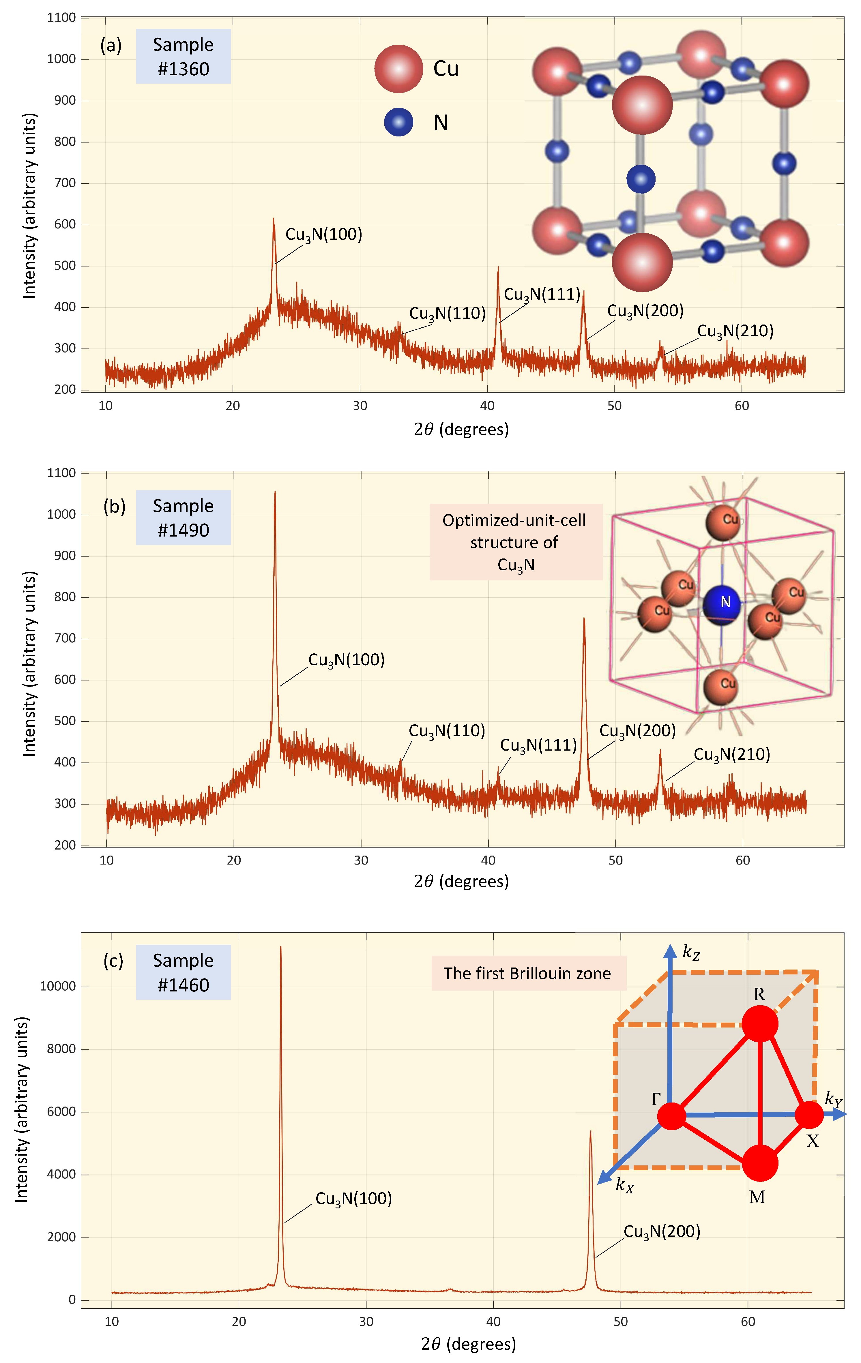
XRD patterns of three as-deposited
thin films are shown in
Figure 1. The main diffraction peaks identified as the
,
, and
crystallographic planes, represent a
polycrystalline film (card number 00-047-1088), in
cubic,
anti-
structure (space group P
, number 221, first reported by Juza and Hahn [
24]). No evidence whatsoever for Cu-phase and CuO formation was found in the present XRD diagrams.
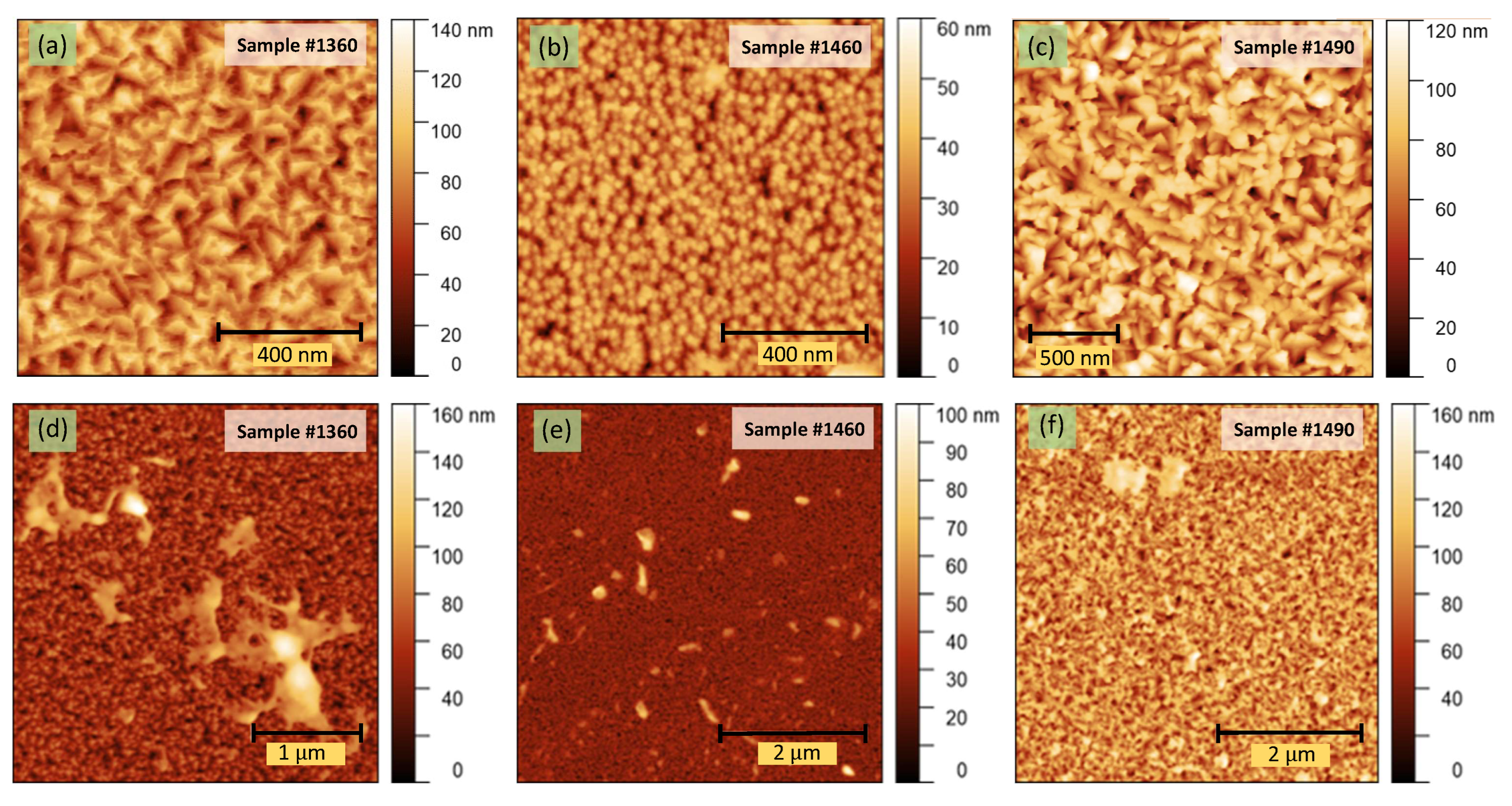
As it was previously said, the surface morphology of the
thin-film samples was carefully analyzed by AFM microscopy.
Figure 2 displays the
and
bi-dimensional AFM micrographs of the three
layers, sputtered all of them at a
total gas pressure of
.
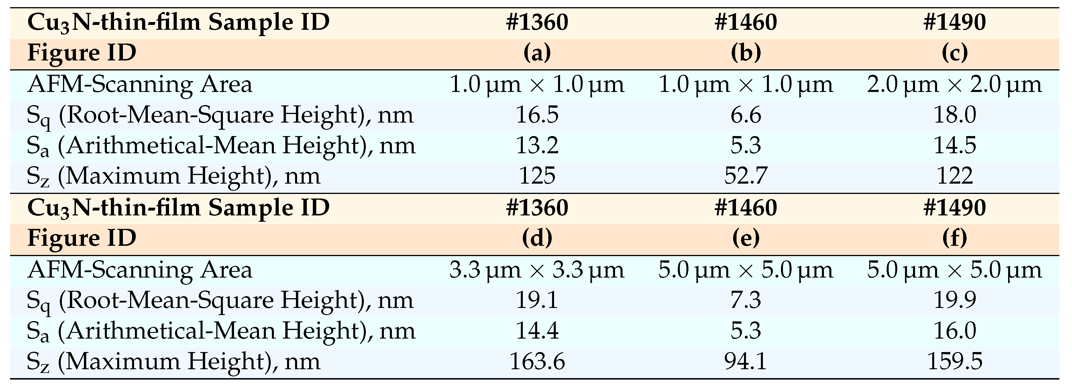
Table 2 indicates the values of the three considered surface-roughness parameters, S
q, S
a, and S
z, respectively, determined with the help of the software connected with this device, and by using 2D-AFM images displayed in
Figure 2. It should be stressed that all these calculations led to an estimated uncertainty of less than around
. According to the three measured surface roughness parameters, S
q, S
a, and S
z, respectively, the
as-deposited thin-layer samples under study do certainly exhibit a
relatively large surface roughness.
It is reasonable therefore that the corresponding obtained values by the ellipsometric models for the BEMA surface-roughness layer,
(see
Table 3), be
larger than those determined by the
and
AFM images. That is, taking into account the fact that the size of the light-spot of the spectroscopic ellipsometer is very much bigger than that of the previous AFM images, it is indeed likely to occur that
is larger than the three parameters
,
, and
, respectively.
Figure 3, on the other hand, shows cross-sectional-view SEM images of the as-grown
thin layers, deposited in a
environment (
Figure 3a), in the particular case of the sample
, and without Ar in the case of sample
. The SEM-measured values of the film thickness clearly confirm the excellent accuracy of the layer thickness calculated by UV/visible/NIR spectroscopic ellipsometry, as will be shown in detail below. The SEM images also corroborated that film surface were not extremely rough and nonuniform, and are mainly made up of typical
columnar grains, typical of the present sputtering deposition technique [
27]. Importantly, all the results found by the SEM microscopy are certainly consistent with those obtained from the previous AFM-microscopy analysis.
Also, in order to register SEM images revealing the CuN layer texture, micrometric trenches were made transversely to the surface. This was carried out using -ion beam, via a focused ions beam (FIB) module. SEM images were recorded by using secondary electron detectors, 5-kV accelerating voltages, and working distances ranging from 6 to . Furthermore, the chemical composition of the layers were found by using an electron dispersive X-ray spectroscopy module, attached to the electron microscope. EDX spectra were obtained by using electron probes accelerated at 30-kV voltages.
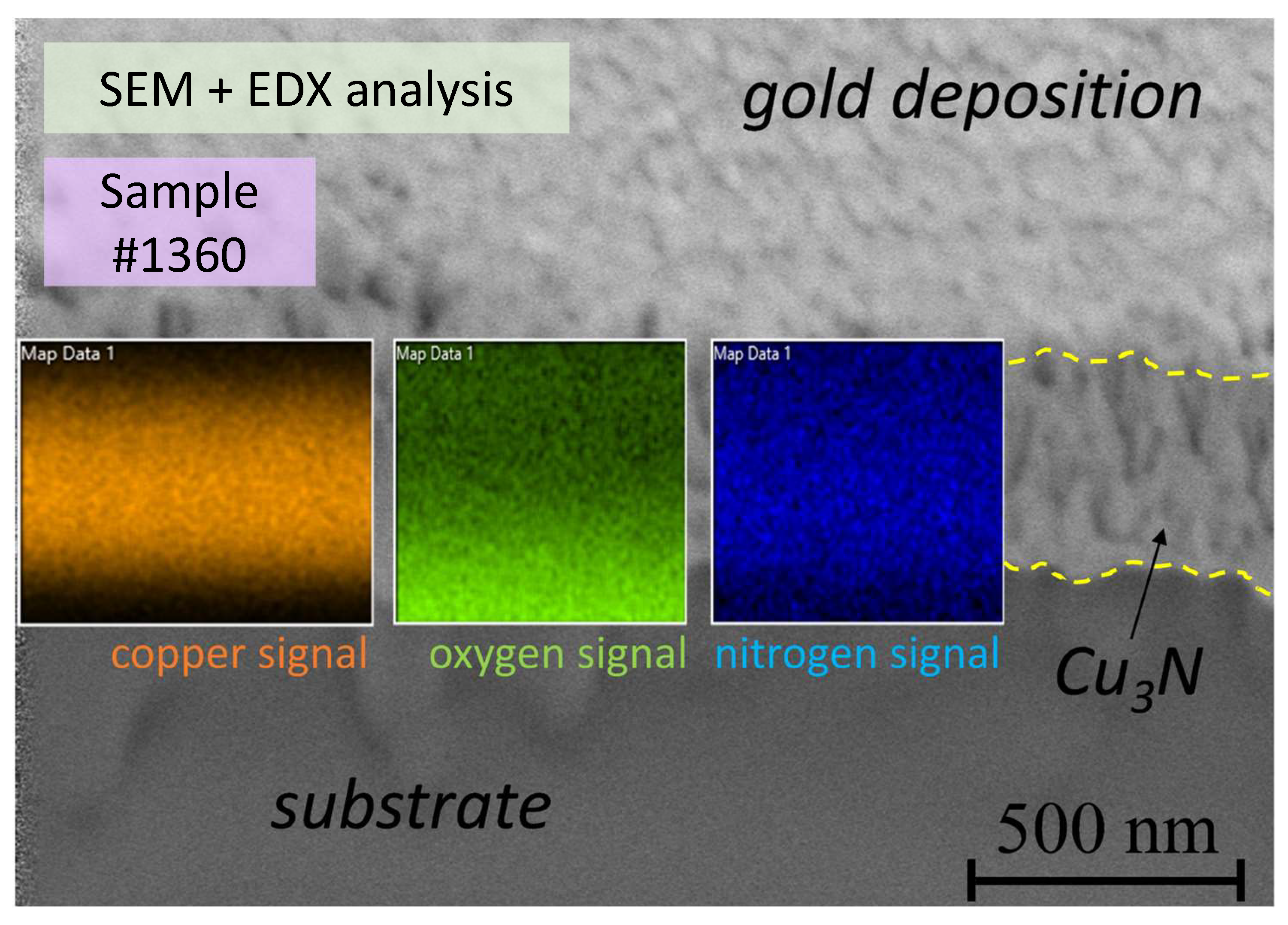
We performed the conventional FIB sample-preparation procedures, before undertaking the EDX analysis. In our EDX study of the present
thin-film specimens (see the measured EDX maps displayed in
Figure 4), oxygen and nitrogen, as light elements, were
not detected with high sensitivity, but it can be observed that the oxygen signal is, indeed, more intense near the glass-substrate region (the glass having both silica and alumina). The nitrogen signal, on the other hand, notably decreases near the
-glass interface, and increases, on the contrary, in the
bulk layer. However, it must be pointed out that an increase of oxygen content and a decrease of nitrogen content near the surface of the film is
not seen. Significantly, from the present EDX maps (
Figure 4), it is
not reasonable to speculate with the existence of a very-thin-copper-oxide layer, at the surface of the
thin film.
4. WVASE®-model ellipsometric fitting
In order to determine the optical constants,
n and
k, of the
thin films, a commercial software package (WVASE32 version 3.774, J.A.Woollam), is used to construct a suitable model in order to fit the ellipsometric data
and
, respectively. It is certainly well-known that an
ideal thin film must be homogeneous and have a perfect flat surface, and that very infrequently happens in reality. The most-usually found cases are obviously
non-ideal thin films, with a surface roughness at top, thickness non-uniformity, and a optical-constant variation from the top, down to the bottom, through the whole thin-film thickness [
23].
The two ellipsometric parameters
and
, respectively, are related to the ratio of the Fresnel reflection coefficients,
and
, for p- and s-polarized light, respectively, as expressed in Eq.(1):
The ratio,
, of the two values is measured by the VASE technique, and, as consequence, the obtained values are very accurate and reproducible [
23]. For the present thin-film sample under study (a
thin film onto a thick-transparent-glass substrate), the Sellmeier dispersion function is employed in order to describe the optical properties of the transparent glass substrate. In the optical model for the
thin film, such a film is divided into two equivalent parts.
One of them is a
bulk planar
layer, and its corresponding bulk thickness is denoted by
. The other one is a surface-roughness layer consisting of a mixture of air void and
material; the thickness of the vertical surface roughness is denoted by
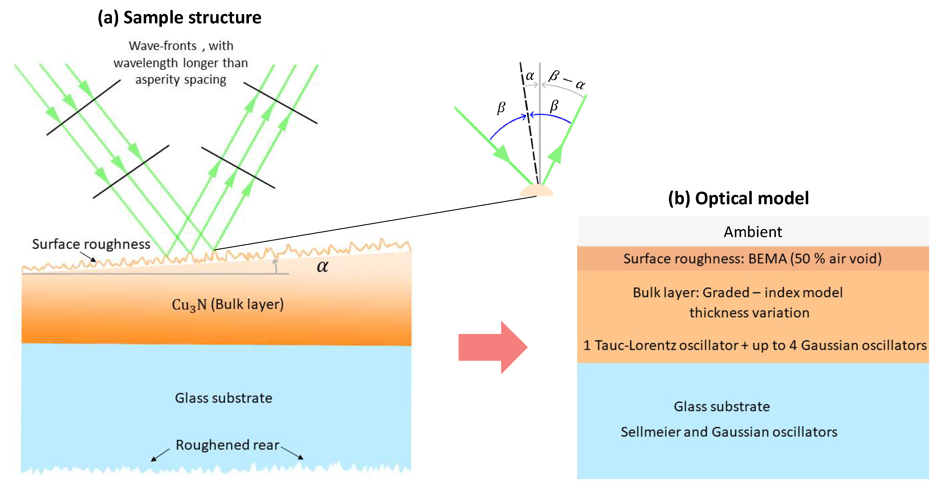
. To clearly illustrate the proposed model, a schematic sketch of this model is shown in
Figure 5. For the surface-roughness layer, a Bruggeman-effective-medium approximation is commonly appropriate, whereby the medium consists of the mixture of
of air void and
material, and where it is verified that
. For the
layer (with thickness
), the Tauc-Lorentz (TL) and Gaussian (Gau) oscillators were successfully adopted to accurately described the complex dielectric function of the
material [
22,
28]. The ‘TL’ and ‘Gau’ oscillator functions are given by Eqs. (2)-(5), respectively [
23]:
where
and
In Eqs. (2) and (3), the subscript ‘T-L’ encompasses the fact that this particular dispersion model is based upon the Tauc joint density of states, and the Lorentz oscillator. The four fitting parameters are: , , and , respectively, and where these parameters are all of them expressed in eV. Here, stands for the Cauchy principal value of the two previous integrals.
The ‘Gau’ oscillator function, on the other hand, is given by the following expression:
where
and
and, finally,
The three fitting parameters that are employed for the WVASE® fitting in this particular case are , where the corresponding unit is dimensionless, , where the unit is eV, and , where the unit is also eV.
Another ellipsometric model which will be employed in this analysis is the aforementioned BEMA model. This model makes the
self-consistent choice of the
host-material complex dielectric function equals to the final
effective complex dielectric function of the multi-constituent material. The BEMA model requires the numerical solution of the following equation, for two constituents A and B, respectively:
For the glass substrate the expression for the dielectric function is as follows:
It is the so-called Pole or Sellmeir term, which corresponds to a Lorentz oscillator with zero broadening. Some gaussian oscillators will also be added in order to complete the accurate description of the Corning® transparent glass substrate used.
It is worth pointing out that several studies have reported that the variation of the two optical constants,
n and
k, respectively, of a thin film along the normal direction to the film, is most frequently owing to the drifting of the deposition-process parameters [
27]. This fact suggest that the optical model with an one-dimensional graded index, along the normal direction to the thin layer, can reasonably be adopted in the present case.
Graded layers work by introducing a series of homogeneous layers, whose optical constants slightly-and-gradually change in each of the successive layers.
Figure 5a displays a very detailed and realistic schematic of a
thin film onto a bare transparent glass substrate.
Figure 5b, on the other hand, is the suggested model to accurately fit the measured
and
parameters, where a BEMA model with 50-%-of-air-void is employed in order to give an account for the effect of the existing
rough surface; a one-dimensional graded-index model throughout the whole film, from the bottom to the top, combined with one T-L oscillator and up to four Gau oscillators are employed in order to fully describe the three
-bulk-flat layers under study. Furthermore, two zero-width oscillators, and two additional Gau oscillators are adopted in order to accurately describe the Corning
®-glass transparent substrate employed in our RF-magnetron-sputtering depositions.
Next, we must first define some convenient statistical quantity, which is called a
maximum likelihood estimator. We will elaborate now a little bit more about that aspect by stating that the principle of maximum likelihood assumes that the population sample is a fair representation of the whole population, and selects a correct estimator that maximizes the probability density function (in continuous cases), or the probability mass function (in discrete cases). This particular choice represents the level of accuracy in correctly matching the data obtained from the
constructed optical model, to our experimentally-measured data [
29]. It has to be mentioned that the parameters of the particular oscillators were all appropriately varied in the process. This maximum-likelihood estimator must be necessarily positive, and go down to zero (or, at least, go down to an
absolute minimum), when the model-generated data
exactly matches the experimentally-measured data. The present Woollam WVASE32 software employs the following mean-square error (MSE) estimator:
where
N is the number of (
) ellipsometric-angle pairs,
M is the total number of
free fitting parameters in the adopted optical model, and the introduced values of
are the corresponding standard deviations associated to all the collected, measured data points. Another very common estimator, the so-called
chi-square,
, is introduced in Eq.
11, for the sake of illustration.
The measured and simulated values of
and
, at the three selected angles of incidence of
,
, and
, respectively, in the UV/Visible/NIR wavelength range from 300 up to
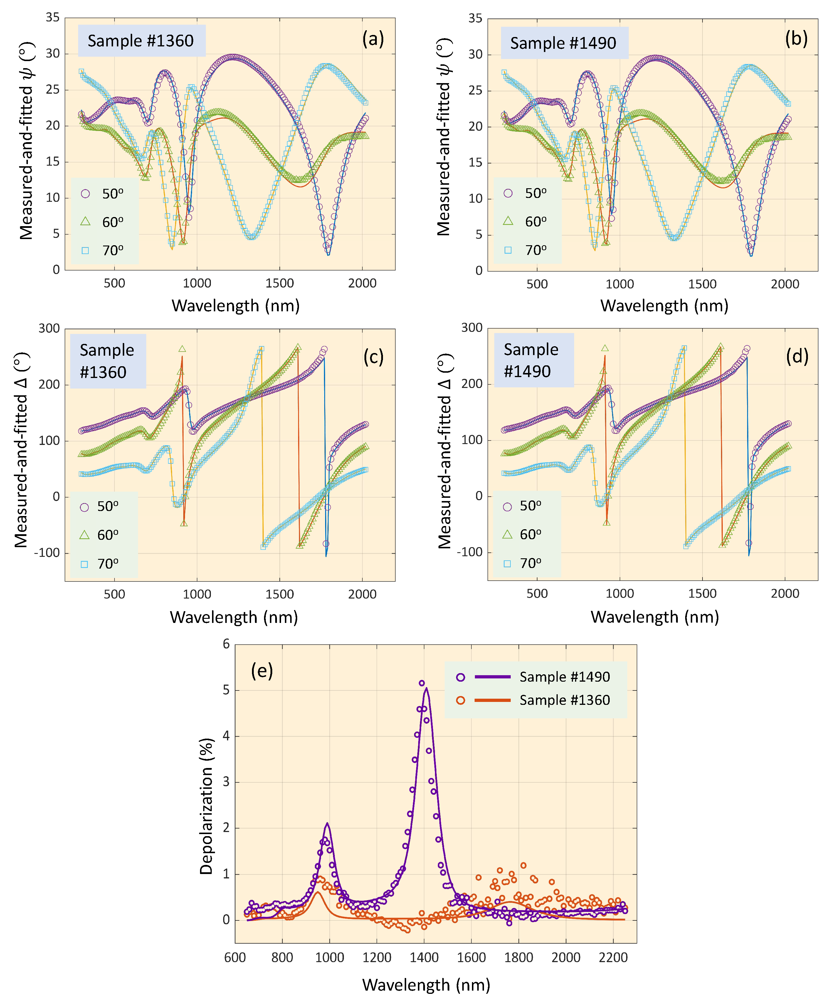
, are depicted in
Figure 6a-d. It can clearly be noticed that excellent fitting results are obtained for both ellipsometric parameters,
and
, respectively. By the optimization process carried out, it is found that the best fitting results are achieved with: (
i) a graded-index variation from bottom to top of aproximately
to
, and (
ii) thicknesses of the
bulk layer and surface-roughness layer,
and
, of around 310 to
and close to 20 to
, respectively, all of them in close agreement with those estimated values from the independent SEM and AFM measurements (see
Figure 2 and
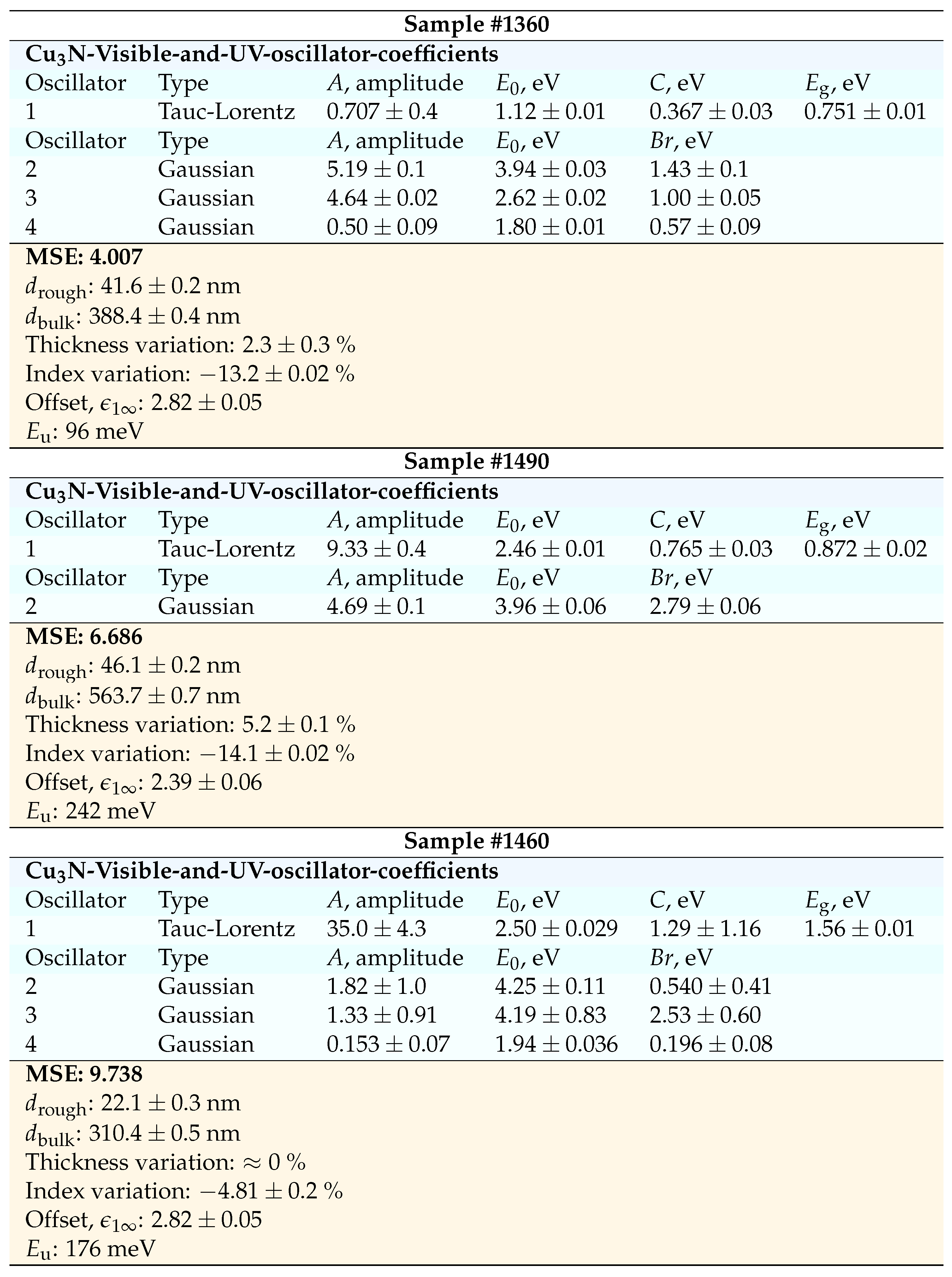
Figure 3). Lastly, the calculated parameters belonging to the best fit for each Cu
N sample, and those experimentally-measured values, are all of them listed in
Table 3. It has also been found that, if either the adopted graded-index model was
not included, or all the oscillators are fully-chosen T-L oscillator, the associated fitting results are notably worsened, causing an incorrect derivation of the optical constants. Contrarily, if all the oscillators are adopted Gau oscillators, the resulting optical constants are just slightly affected.
It is next shown that a measurable
depolarization effect has clearly been observed in all the specimens. To begin with, it must be said that depolarization does occur if the reflected beam contains multiple polarization states. In the case of
isotropic samples —as we assume in our case of the copper-nitride thin films— depolarization,
D, can be calculated from the values of the two ellipsometric angles,
and
, respectively, as follows:
Depolarization spectra of the
samples were measured by also employing the Woollam VASE ellipsometer, in the spectral range of 300-
; some of these spectra are shown in
Figure 6e. Evaluation of the depolarization spectra was also performed with the WVASE32 software.
6. Conclusions
(i) In the present investigation, polycrystalline CuN thin films were deposited by making use of RF-magnetron sputtering, at room-temperature, a total pressure of , and by using two different gaseous environments of and , respectively. The XRD patterns showed that the thin films exhibited an anti- structure. In order to enrich the depth of the analysis of the semiconductor material, AFM, SEM (by using FIB sample preparation), and EDX measurements, were systematically performed in all the RF-sputtered thin layers.
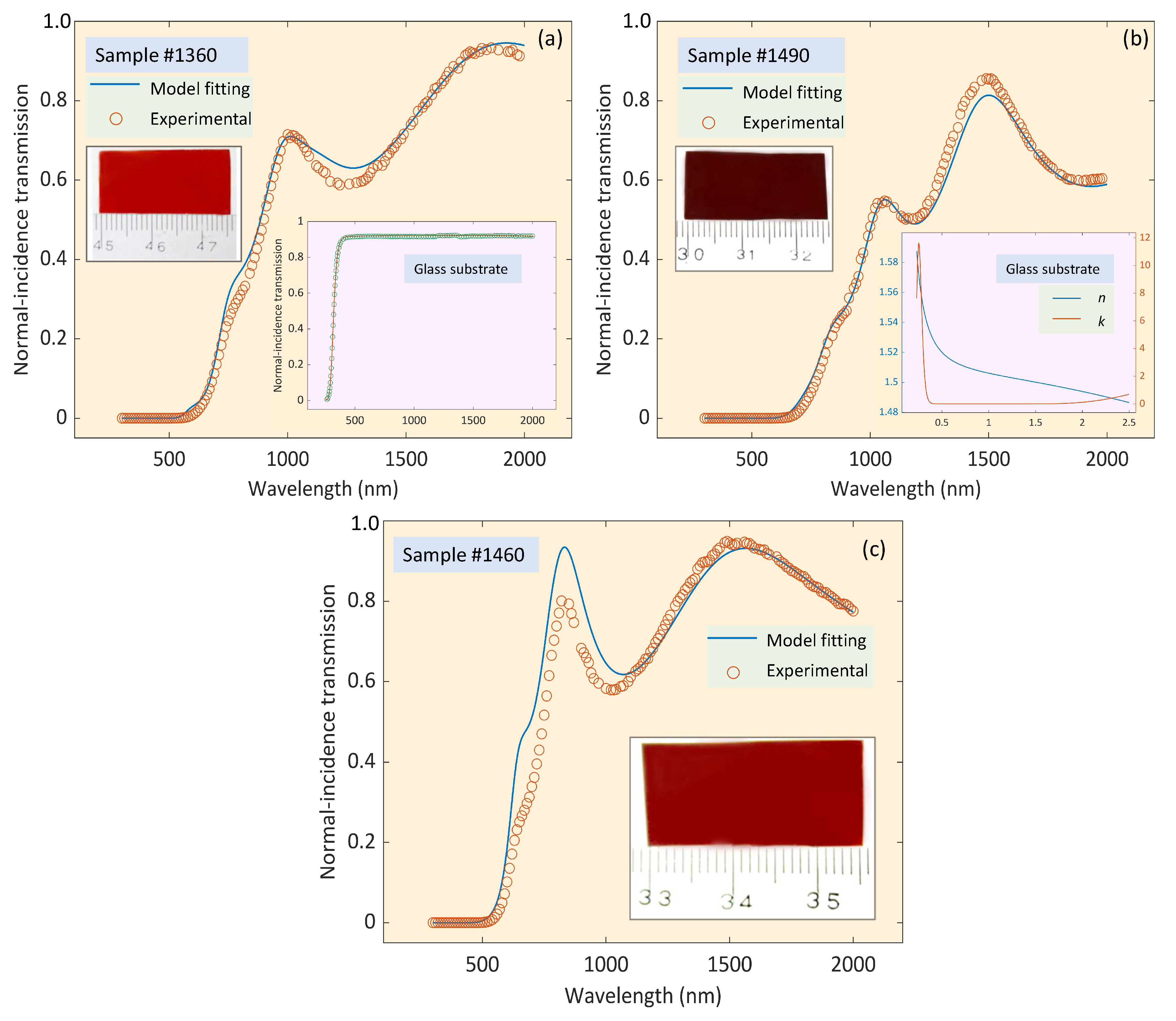
(ii) The complex refractive index of the RF-sputtered thin films was accurately determined via VASE measurements, at three angles of incidence, , , and , respectively. The constructed ellipsometric model consisted of a one-dimensional graded-index plus a BEMA model with -air-void, in order to describe both, the bulk layer and the rough surface. The experimentally-measured, normal-incidence transmission spectrum, and the predicted transmission spectrum based upon the obtained ellipsometric results, show a reasonably good agreement in all the cases. The calculated optical constants allow to be able to design and simulate a potential photovoltaic electronic device. The absorption strength, on the other hand, reaches a magnitude of from approximately , suggesting a very promising potential for solar-cell applications. The lower Urbach energy value, for the case of the sample #1360 with a gaseous environment of , is associated with the presence of much lower level of defects in its atomic structure, in comparison with the samples of a gaseous environment of just N.
(iii) Last but not the least, the investigated material with the corresponding values of can unambiguously be considered satisfactory for use as a solar-light absorber material. The specific aspect of the solar-cell technology that could certainly benefit the most from the use of the CuN thin-film material would be that related to the photovoltaic electronic devices, as they provide a flexible texture, and are relatively inexpensive in order to be manufactured.
Figure 1.
X-ray diffraction (XRD) patterns of the three copper nitride thin films, deposited onto glass substrates, and corresponding specifically to (a) specimen
, (b) specimen
, and (c) specimen
. The 3D cubic structure of Cu
3N is clearly illustrated as an inset in
Figure 1b. This cubic structure of the
unit cell contains six Cu atoms, and their fractional coordinates are the following:
,
, and
. The fractional coordinate of the N atom is
, which is in the center position of the present Cu molecules[
25].
First Brillouin zone of Cu
3N, with the high-symmetry points
, M
, R
, and X
, labeled and joined by red lines [
26], shown as an inset in
Figure 1c.
Figure 2.
The two-dimensional AFM images of thin-filmS: (a) and (d) Sample #1360, (b) and (e) Sample #1460, (c) and (f) Sample #1490, respectively.
Figure 2.
The two-dimensional AFM images of thin-filmS: (a) and (d) Sample #1360, (b) and (e) Sample #1460, (c) and (f) Sample #1490, respectively.
Figure 3.
High-magnification cross-sectional SEM images of the studied in (a) , (specimen ), and (b) pure (specimen ) environments.
Figure 3.
High-magnification cross-sectional SEM images of the studied in (a) , (specimen ), and (b) pure (specimen ) environments.
Figure 4.
Cross-sectional energy-dispersive-X-ray (EDX) spectroscopy elemental mapping, by using scanning electron microscopy (SEM) of copper nitride thin films, grown by RF-magnetron sputtering, on transparent glass substrates, at room temperature. We have previously performed the FIB sample preparation, before making the EDX measurements.
Figure 5.
(a) Schematic diagram of the sample structure under study, consisting of a copper nitride thin film onto a transparent glass substrate, with the rear surface roughened. (b) Adopted model for the fitting carried out in the present ellipsometric analysis.
Figure 5.
(a) Schematic diagram of the sample structure under study, consisting of a copper nitride thin film onto a transparent glass substrate, with the rear surface roughened. (b) Adopted model for the fitting carried out in the present ellipsometric analysis.
Figure 6.
(a) and (b) the measured-and-fitted -values at the three angles of incidence of , , and , in the wavelength range from up to . (c) and (d), the measured-and-fitted -values at the same previous angles and in the same previous experimental spectral range.(e) Depolarization spectra of the two representative copper nitride thin films at the angle of incidence of . The curve fitted by employing the ellipsometric method described in-depth in the text; is also presented with a solid line. The depolarization has been modeled with and thickness nonuniformity in the cases of sample and , respectively.
Figure 7.
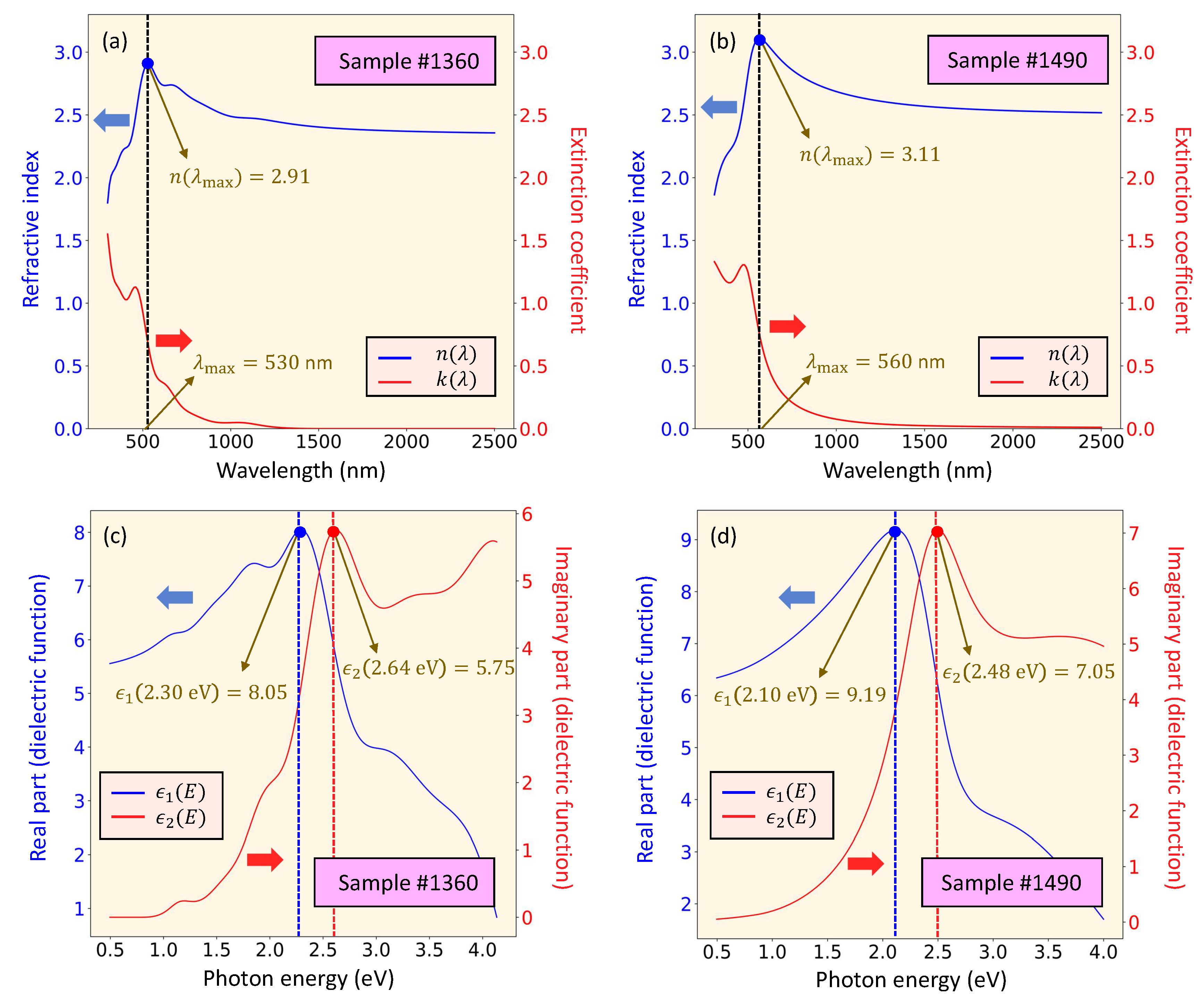
(a) Real part of the complex refractive index, n, and (b) imaginary part of the complex refractive index, k, of the thin layers. (b) The real, , and imaginary, , parts of the complex dielectric function.
Figure 7.
(a) Real part of the complex refractive index, n, and (b) imaginary part of the complex refractive index, k, of the thin layers. (b) The real, , and imaginary, , parts of the complex dielectric function.
Figure 8.
Experimentally-measured optical-transmission intensity data, acquired by using the varied-angle spectroscopic ellipsometer, and the computationally-predicted values of transmittance in the studied spectral range: (a) sample #1360, (b) sample #1490, and (c) sample #1460.
Figure 8.
Experimentally-measured optical-transmission intensity data, acquired by using the varied-angle spectroscopic ellipsometer, and the computationally-predicted values of transmittance in the studied spectral range: (a) sample #1360, (b) sample #1490, and (c) sample #1460.
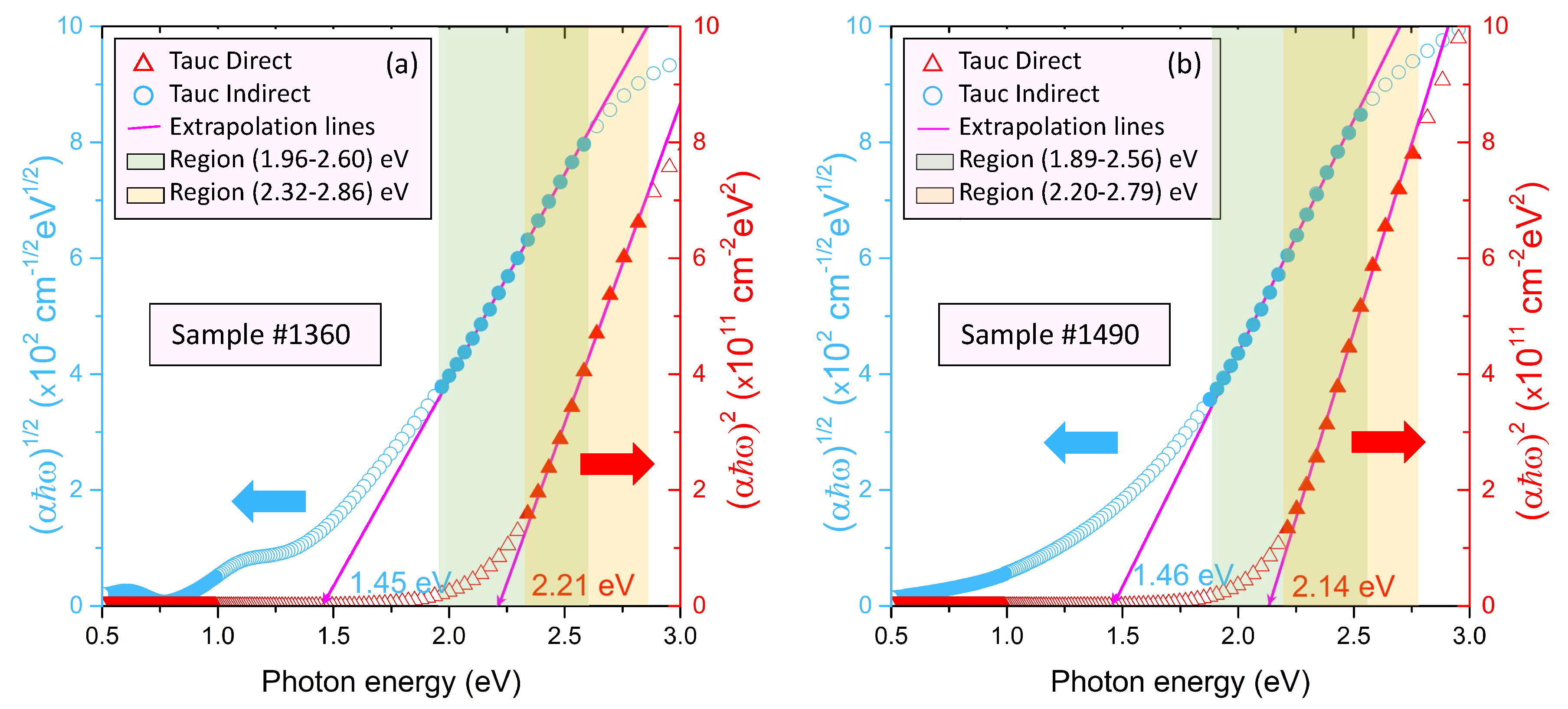
Figure 9.
versus plot for the determination of the indirect energy-band gap, and versus plot for the calculation of the direct energy-band gap, for the samples (a) #1360, and (b) #1490, respectively.
Figure 9.
versus plot for the determination of the indirect energy-band gap, and versus plot for the calculation of the direct energy-band gap, for the samples (a) #1360, and (b) #1490, respectively.
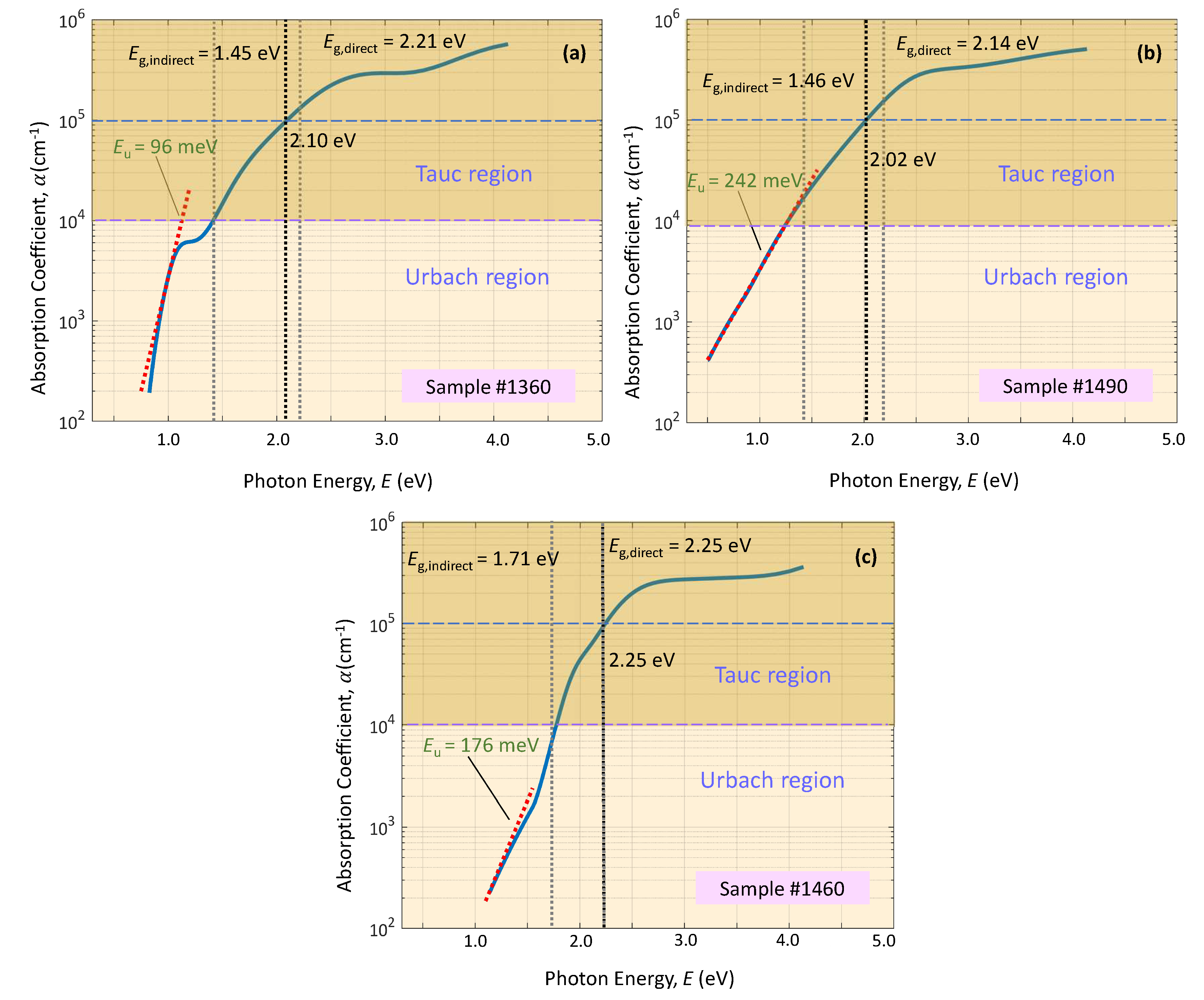
Figure 10.
A semilogarithmic plot of the absorption coefficient as a function of incident photon energy for copper nitride thin films grown on glass substrates. The exponential dependence is valid in the near band-edge region. The slope of the linear fit is used to calculate the Urbach-energy parameter, .
Table 1.
Deposition conditions for the growth of CuN by RF-magnetron-sputtering deposition.
Table 1.
Deposition conditions for the growth of CuN by RF-magnetron-sputtering deposition.
Table 2.
Surface-roughness parameters determined from AFM and images of the copper nitride thin layer, grown by RF-magnetron sputtering on glass substrates.Values of the root-mean-square height, Sq, the arithmetical-mean height, Sa, and the maximum height, Sz, corresponding to the two representative thin-film samples.
Table 3.
Deposition conditions of the layers. The values of best-fit parameters obtained by employing the VASE ellipsometer (J.A.Woollam Co.), and their corresponding experimental uncertainties.
Table 3.
Deposition conditions of the layers. The values of best-fit parameters obtained by employing the VASE ellipsometer (J.A.Woollam Co.), and their corresponding experimental uncertainties.
