Preprint
Communication

Transition From Screw Type to Edge Type Misfit Dislocations at InGaN/GaN Heterointerfaces

Altmetrics

Downloads

147

Views

68

Comments

0

A peer-reviewed article of this preprint also exists.

Submitted:

24 May 2023

Posted:

25 May 2023

You are already at the latest version

Alerts
Abstract
We have investigated the interfacial dislocations in InxGa1–xN/GaN (0 ≤ x ≤ 0.20) heterostructures using diffraction contrast analysis in a transmission electron microscopy. The analysis indicate that the structural properties of the interface dislocations depend on the indium composition. For lower indium composition up to x = 0.09, we observed that the screw-type dislocations and dislocation half loops occurred at the interface even though the former do not contributes toward elastic relaxation of the misfit strain in the InGaN layer. With the increase of indium composition (0.13 ≤ x ≤ 0.17), in addition to the network of screw-type dislocations, edge-type misfit dislocations were found generated with their density gradually increasing. For higher indium composition (0.18 ≤ x ≤ 0.20), all the interfacial dislocations are transformed into a network of straight misfit dislocations along the <10-10> directions leading to partially relaxation of the InGaN epilayer. The presence of dislocation half loops may be explained by slip on the basal plane, the formation of misfit dislocations are attributed to punch-out mechanism.
Keywords: 
Subject: Chemistry and Materials Science  -   Materials Science and Technology

1. Introduction

The direct bandgap of InGaN alloys has been attracting tremendous research attentions due to their excellent emission properties for light-emitting diodes and laser diodes [1,2]. However, several critical issues related to epitaxial growth remain unsolved [3]. This is mainly due to large lattice mismatch of up to ~11% between GaN and InN, which results in compositional instability in InGaN [4]. Therefore, solving the lattice mismatch has become an important prerequisite for the high-quality InGaN epilayer growth, and it is urgently needed to achieve high efficiency and high luminescence in green light emitting devices [3]. During the heteroepitaxial growth of InGaN thin films on GaN buffers, large lattice mismatches lead to huge strains, resulting in plastic relaxation of misfit strain. This has been evidenced as occurrence of parallel networks of straight misfit dislocations aligned along with <10-10> orientations in compressively strained InGaN/GaN [5,6,7,8,9] as well as in tensile strained AlGaN/GaN [10] heterostructures. III-nitride epilayers grown on (0001) substrates suffer from the absence of primary gliding planes due to the lack of resolved shear stress, and possible plastic strain relaxation needs the activation of secondary glide planes. The origin of the misfit dislocations is ascribed to internal and external factors, for example, growth surface steps [11,12], use of ELOG GaN substrates [5], from pre-existing threading dislocations in the substrate as reported by Mathews [13,14,15,16]. Different theoretical models based on force-equilibrium [17] or energy-balance equations [18] including that of Matthews-Blakeslee and Fischer [13,19] are used to account for the generation of misfit dislocations via glide process. Formation of misfit dislocations is first attributed to its nucleation at the surface, followed by its glide to the heterointerface on {11-22} pyramidal planes [5]. In this study, we have found that in the strain relaxation process only a part of the heterostructure is fully strained, while the other parts are partially relaxed. In this paper, we have investigated transition from screw type to edge type misfit dislocations in the InxGa1-xN/GaN heterostructures grown on (0001) sapphire substrates with indium composition in the range of 0 to 20%.

2. Materials and Methods

A series of metal organic vapor phase epitaxy grown InGaN/GaN heterostructures with varying indium composition was used in this study. The InGaN layers were grown at temperatures between 700 oC and 730 oC. The varying indium composition of InGaN epilayers was determined by high-resolution X-ray diffraction technique. The thickness of corresponding InGaN epilayers was measured between 40 and 110 nm by the cross-sectional transmission electron microscopy (TEM) imaging. Structural properties of interface dislocations were investigated by dark-field TEM diffraction contrast analysis and by High-resolution TEM. Here, plan-view specimens used in the TEM analysis were prepared by a two-step process: tripod wedge mechanical polishing of the specimens to 12 µm, followed by ion milling (Gatan PIPS) at -40 oC with 5 keV Ar+ gun incident at 5o angle to the specimen surface until the electron transparency was reached. The observations along [0001] zone axis were performed in the TEM operating at an accelerating voltage of 200 kV.

3. Results and Discussions

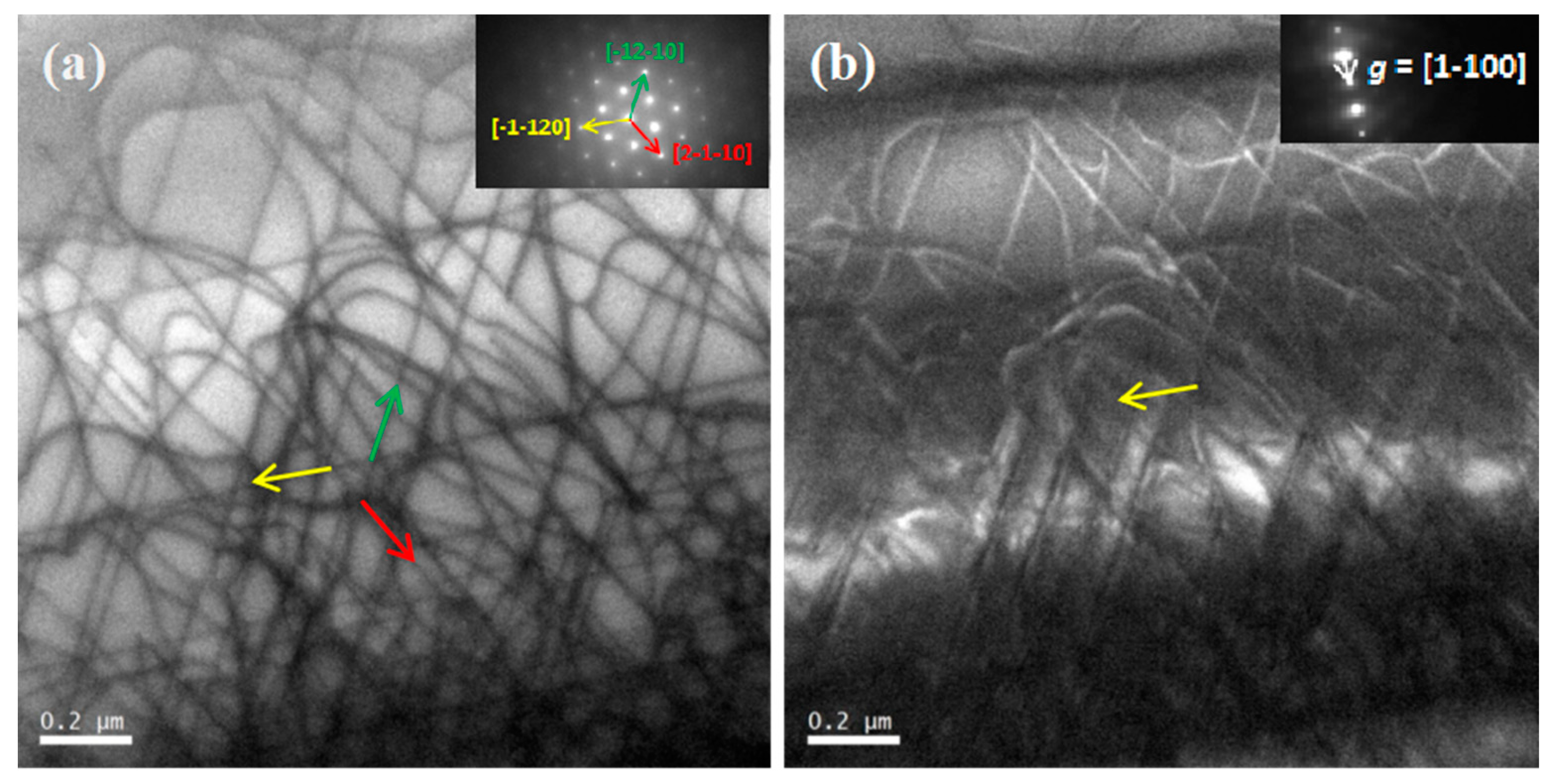
Without indium composition, no defects were found in plan-view samples (not shown here). Figure 1a,b exhibit [0001] zone axis and [1–100] dark field plan-view TEM images of In0.09Ga0.91N/GaN heterostructure, respectively. A network of straight dislocation lines and dislocation half loops at the interface can be observed in Figure 1a. These dislocation lines extend over several micrometers in the entire observable area with an average inter-line spacing of 100 nm. The three sets of dislocation lines are aligned along with the <11-20> directions, which can be assessed from the selected area diffraction pattern for zone axis [0001] in the inset of Figure 1a. The Burgers vectors of these dislocations can be identified by TEM diffraction contrast analysis [20]. As shown in the dark field image (see Figure 1b) taken under g = [1–100] diffraction condition from the same area, we observe that only those set of dislocation lines along [–1–120] direction (yellow arrow) disappears, indicating that these dislocations satisfy the invisibility criterion g . b = 0. Therefore, the Burgers vector b of this set of dislocations is a = 1/3[-1-120], which is parallel to the dislocation line orientation, and are identified as screw ones. The other two sets of dislocations are also verified as screw ones according to the same method. Thus, all the interface dislocations in In0.09Ga0.91N/GaN heterostructures are identified as pure screw dislocations with b = a. The occurrence of screw dislocations is unusual as it well known that the screw dislocations cannot relax the strain of the film.
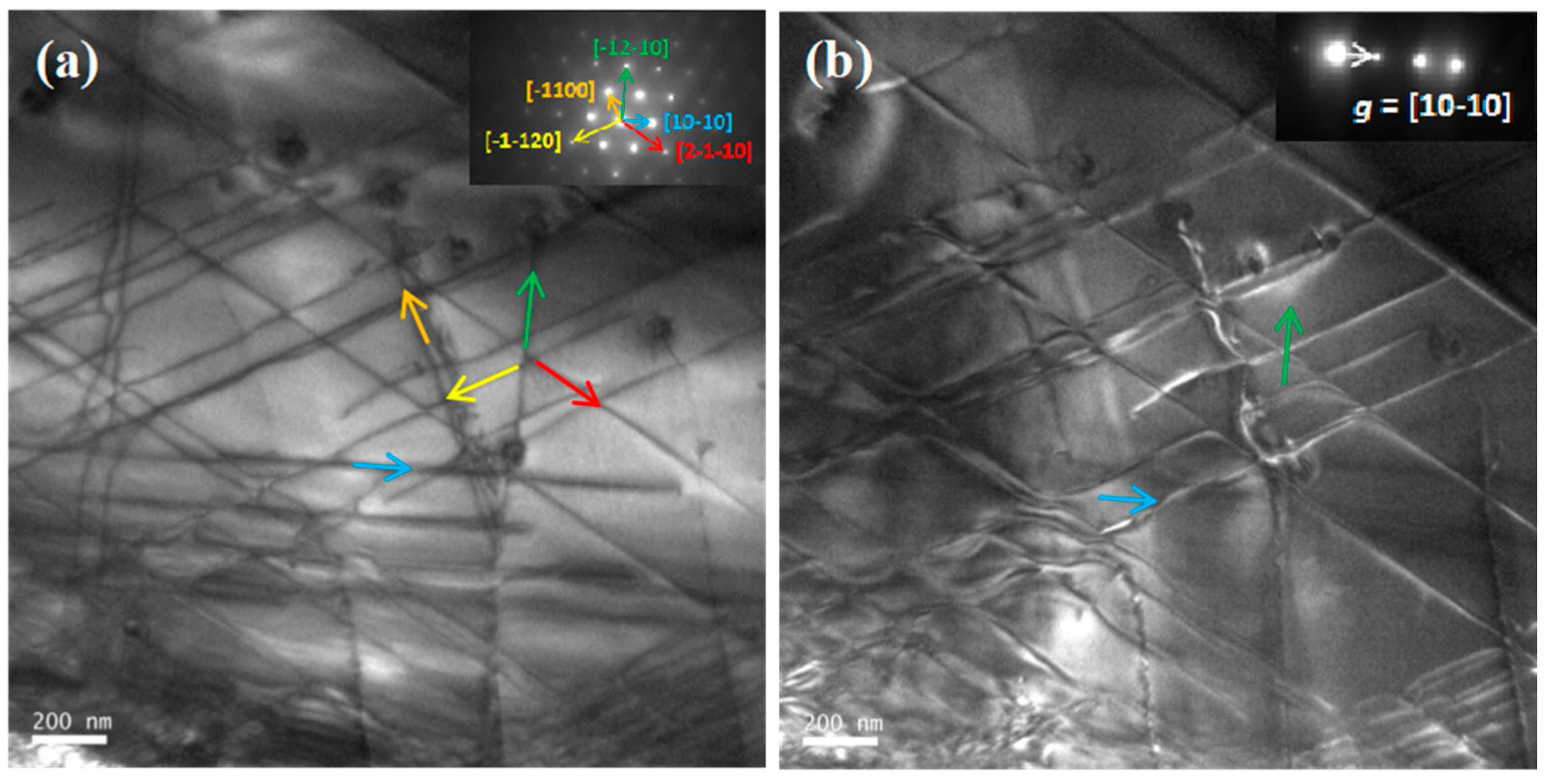
Also for higher In-content of 17%, a network of dislocation lines with an average interline spacing of 200 nm can be seen in the dark-field images obtained at g = [10-10] (see Figure 2a). The three sets of dislocation lines are aligned along with the <11-20> directions and two sets of dislocation lines are along with the <10-10> directions. The dark field image for g = [10-10] of the same area (Figure 2b) shows that one set of dislocation lines along [-12-10] direction (green arrow) disappears. Hence, b = a = 1/3[-12-10] for these dislocations in the direction parallel to the dislocation line. These dislocations are again identified as screw ones. Similarly, the other two sets of dislocations (yellow and red arrows) along the equivalent <11-20> directions are also verified as screw-type ones. We also found that one set of dislocation lines that are along [10-10] direction (blue arrow) also become invisible under this beam condition, which means its b = a = 1/3[-12-10], i.e. perpendicular to the dislocation line direction. Hence, this set of dislocations are identified as edge-type dislocations, i.e., misfit dislocations (MDs). The other set of dislocation (orange arrow) along equivalent <10-10> direction is also verified as MDs. Thus, for In = 17%, all the observed dislocations have Burgers vector of a, with most of them are screw dislocations along <11-20> and the remaining are MDs along <10-10> directions.
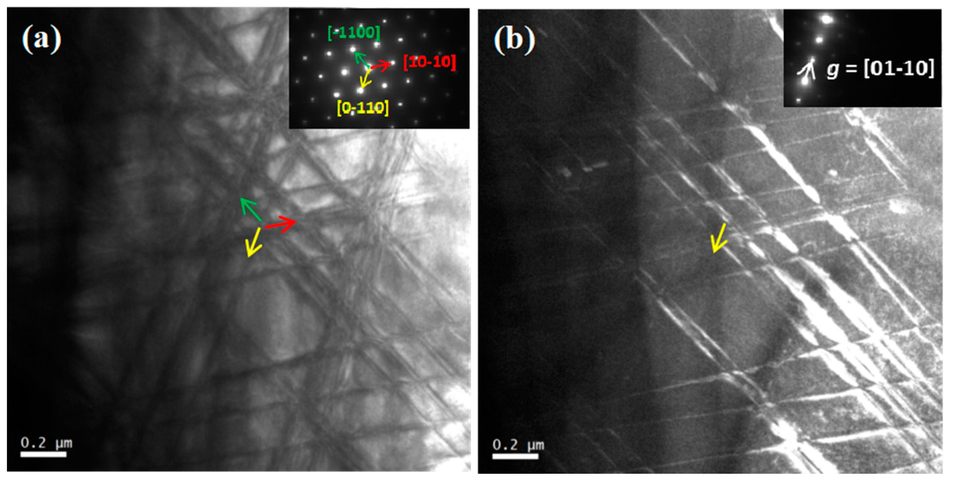
When we go further higher in In-content (In = 20%), unlike the previous two cases only one type of network of dislocation lines can be observed in bright filed TEM image (see Figure 3a). The three sets of dislocation lines are aligned along the <10-10> directions with average interline spacing of ~200 nm. In Figure 3b, we observe that one set of dislocation lines along [0-110] direction (yellow arrow) become invisible in the dark field image obtained g = [01-10]. Thus, b = a = 1/3[2-1-10] for these dislocations, which is perpendicular to its line direction, again classifying them as MDs. The other two sets of dislocations (green and red arrows) are also verified as MDs. Thus, all the observed dislocations are pure MDs, which contributes toward relaxation of the lattice mismatch strain. Some of the dislocations were found to dissociate into two separate dislocations which meanders along the same <10-10> direction as shown in Figure 3. Diffraction analysis displayed that the latter were also a-type dislocations. This dissociation indicates that the MDs in such heterostructures could exist with Burgers vector of both a and 2a as reported by Liu and Li et al. [6,8].
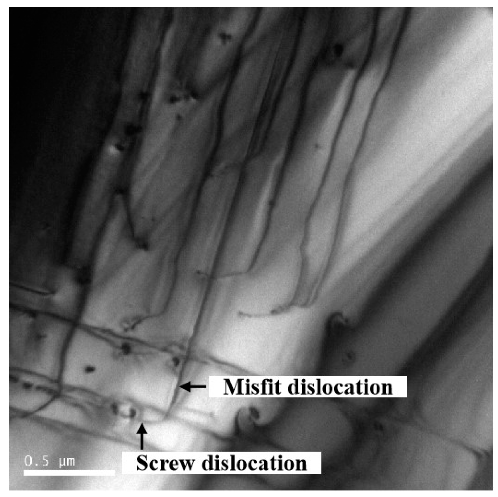
One can realize a particular trend in the occurrence of dislocations from Figure 1, Figure 2 and Figure 3, as the lattice mismatch increases with indium composition from 9% to 20%, the interface dislocations transform from entirely screw dislocations into entirely misfit dislocations. In sample In0.13Ga0.87N/GaN heterostructure, this transformation process is well captured. Figure 4 shows a bright field plan-view TEM image, which exhibits clearly this transformation process of the dislocations from screw type to edge type, detailed analysis is shown in a schematic diagram below. This implies plastic relaxation of the layers gradually replaces elastic relaxation process.
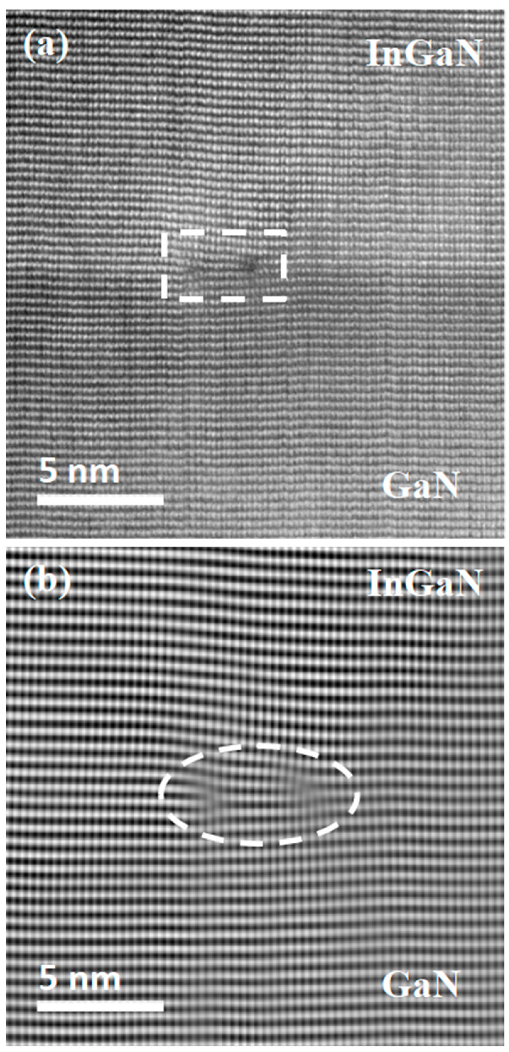
To determine the dislocations in the plan-view TEM images are interfacial dislocations, a high resolution TEM (HRTEM) image of InGaN/GaN heterostructure was taken under [1010] zone axis, as shown in Figure 5a. It can be seen that the plan-view dislocations exist at the heterointerface (marked with the dashed line). Due to the large misfit strain and the presence of indium, the atomic arrangement in the heterostructure cannot be observed clearly in the HRTEM image. In order to facilitate the observa tion of {1120} lattice fringes, we acquired the Fourier filter ing image using in-plane Fourier spots. Figure 5b is a Fou rier filtering image of Figure 5a. We clearly observed in Figure 5b that extra half plane of atoms lie at the interface, therefore these interfacial dislocations are MDs (see the dashed line).
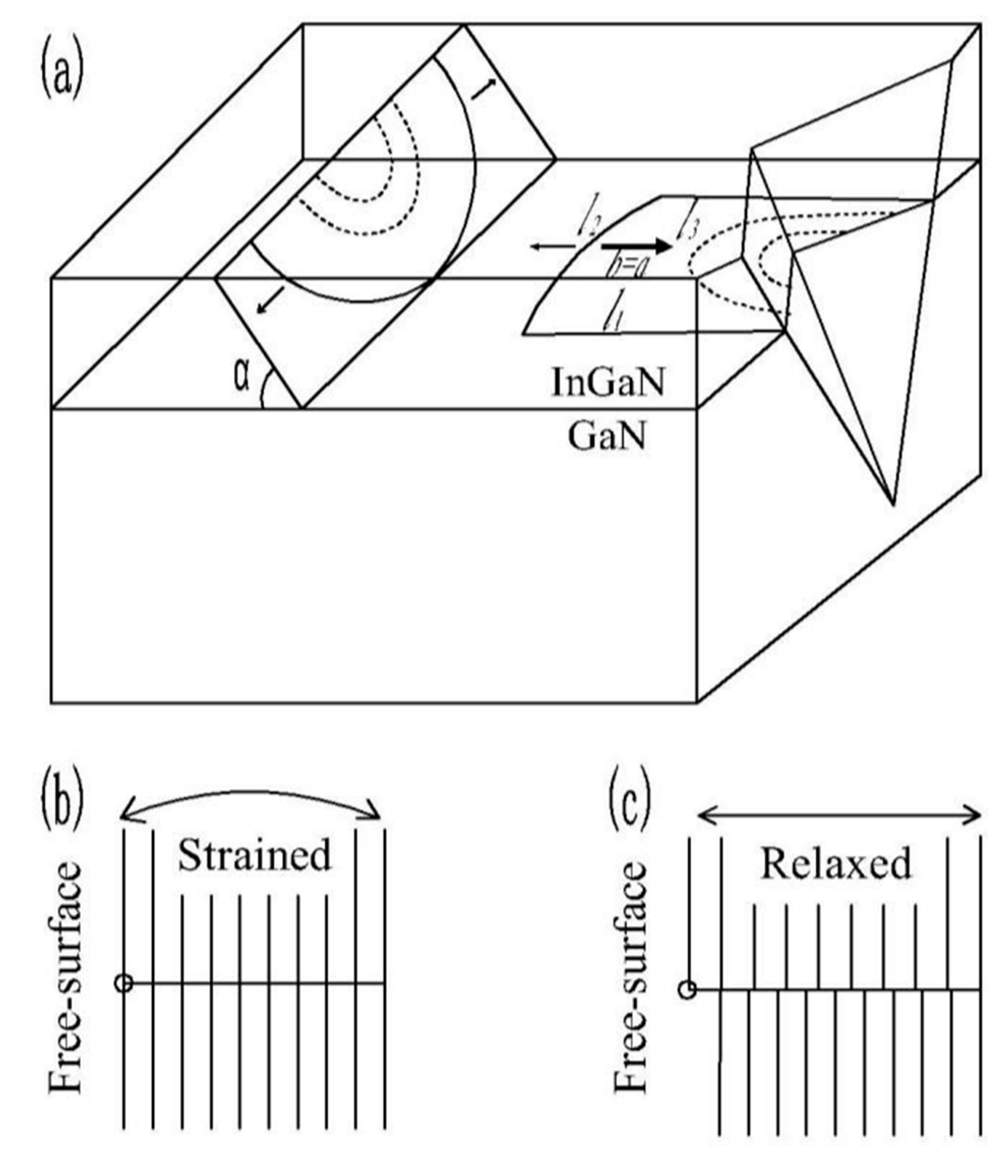
It is commonly understood that the strain occurring due to lattice mismatch between epitaxial layers and substrates is eased to an extent either by elastic relaxation or by plastic relaxation. The mechanisms for strain relaxation observed in the InGaN/GaN system have been reported by Liu et al. [21], as shown in Figure 6. Figure 6a shows a schematic diagram illustrating the formation process of these dislocation half loops and misfit dislocation network. The dislocation half loop can be divided into three line segments: l1, l2 and l3 (right portion of Figure 6a). The Burgers vector (b = a) of the dislocation half loop is parallel to the propagation direction, thus, l1 and l3 are screw dislocations (elastic relaxation) and l2 is an edge dislocation (plastic relaxation), namely, a misfit dislocation (ignoring the curvature of the segment). Nucleation and propagation of the dislocation half loop happens at the corner of the pit in the process that is driven by the misfit stress. This mechanism is illustrated by schematic diagrams as shown in Figure 6b,c. At the intersection between the heterointerface and the free surface, the atomic bonding is rearranged because of the misfit shear stress, forming a ledge at the free surface, and an edge type misfit dislocation. Further relief of the misfit strain happens by continuous generation of misfit dislocations. The Burgers vector is in the slip plane, therefore propagation of the dislocation half loops occurs by glide on the basal plane.
Due to a lack of primary gliding planes in the absence of resolved shear stress in InGaN layers grown on GaN (0001), plastic strain relaxation requires activation of secondary glide planes, primary pyramidal ones. As explained by Srinivasan et al. [5], only three of the pyramidal plane systems allows for non-zero resolved shear stress: {1-102}<1-101>, {11-22}<11-23> and {1-101}<11-23>. As they glide within one of the slip systems, three main forces are exerted on them: the lattice misfit stress Fm is the driving force, the line tension Fl and the Peierls force Fp are the resisting forces [22,23,24]. The net driving force for dislocation half loop glide is given by Fnet = Fm FlFp. The first of the three pyramidal planes cannot contribute to dislocation glide due to high Peierls force, while the {11-22}<11-23> slip system is more favorable than {1-101}<11-23> because of large net driving force. It is reported that straight misfit dislocation lines can be generated at InGaN/GaN heterointerface, via slip or punch-out mechanism [6,8], as shown in left portion of Figure 6a. Nucleation and injection of the misfit dislocation network take place in slip system of {11-22}<11-23> [5,6]. The driving force Fd of the process is the resolved shear stress in the inclined {11-22} plane, Fd = Fm cosα. Since the driving force for generating dislocation half loops is larger, Fd = Fm cos0 = Fm. The resisting force for the formation and glide of dislocations on the basal plane is smaller than that for {11-22} planes, namely, the bond density between the basal planes is the lowest. Thus, plastic relaxation via dislocation half loops introduced at the heterointerface is easier than from the growth surface. Whereas interfacial dislocation half loops are restrained by the large dislocation line tension, because the ends of the half loops are pinned at the edge of the pit. The ends of the dislocation half loops are free to move on the growth surface, therefore the dislocation half loops can easily propagate along {11-22}<11-23> slip system and form misfit dislocation network at the interface.
4. Conclusions

We have observed the generation of interface dislocations in InxGa1-xN/GaN heterostructures grown on (0001) sapphire substrates for 0 ≤ x ≤ 0.20. Without indium composition, no defects are found in plan-view samples. For x = 0.09, a network of screw dislocations and dislocation half loops are observed at the heterointerface. For 0.13 ≤ x ≤ 0.17, both the network of the screw dislocations and misfit dislocations are observed with the density of the misfit dislocations increasing gradually. As the indium composition (0.18 ≤ x ≤ 0.20) increases further, all the screw dislocations transform into misfit dislocations with their lines along <10-10> directions. The generation of screw dislocations and misfit dislocations is due to glide of dislocation half loops on the basal plane, the dislocation half loops were introduced from the free surface intersecting the heterointerface. At higher indium composition (x ≥ 0.20), the straight misfit dislocation lines were generated by the punch-out mechanism.

Author Contributions

Conceptualization, Q. T. L. and P. R.; methodology, Q. T. L. and P. R.; software, Q. T. L.; validation, Q. T. L. and Z. M. L.; formal analysis, C. G. and J. T. W.; investigation, Y. B.; resources, P. R. and Q. T. L.; data curation, Q. T. L. and C. G. H.; writing-original draft preparation, Q. T. L.; writing-review and editing, A. M., Y. Z. L. and C. A. W.; visualization, S. L. H. and X. M. G.; supervision, Z. M. L. and P. R.; project administration, Q. T. L.; funding acquisition, Z. M. L. and Q. T. L. All authors have read and agreed to the published version of the manuscript.

Funding

This work was supported by Key-Area Research and Development Program of Guangdong Province (No. 2020B0101320002), the GDAS’ Project of Science and Technology Development (No. 2021GDASYL-20210103074)

Data Availability Statement

Not applicable.

Acknowledgments

The authors thank the GDAS’ Project of Science and Technology Development (No. 2020GDASYL-20200102024, 2021GDASYL-20210103077, 2019GDASYL-0103070 and 2022GDASZH-2022010111), the National Natural Science Foundation of China (No. 62101143 and 62104050). Key Area R&D Program of Guangzhou (No. 202103030002), Guangdong Basic and Applied Basic Research Foundation (No. 2021B1515120022 and 2022A1515110515), Science and Technology Program of Guangzhou (No. 201904020032). The authors would like to gratefully acknowledge the use of facilities at Centre de Recherche sur les Ions, les Matériaux et la Photonique at CNRS.

Conflicts of Interest

The authors declare no conflflict of interest.

References

  1. Nakamura, S.; Mukai, T.; Senoh, M. Candela-class high-brightness InGaN/AlGaN double-heterostructure blue-light-emitting diodes. Appl. Phys. Lett. 1994, 64, 1687. [Google Scholar] [CrossRef]
  2. Ponce, F.A.; Bour, D.P. Nitride-based semiconductors for blue and green light-emitting devices. Nature 1997, 386, 351–359. [Google Scholar] [CrossRef]
  3. Ponce, F.A.; Srinivasan, S.; Bell, A.; Geng, L.; Liu, R.; Stevens, M.; Cai, J.; Omiya, H.; Marui, H.; Tanaka, S. Microstructure and electronic properties of InGaN alloys. Phys. Status solidi (b) 2003, 240, 273–284. [Google Scholar] [CrossRef]
  4. Ho, I.-H.; Stringfellow, G.B. Solid phase immiscibility in GaInN. Appl. Phys. Lett. 1996, 69, 2701–2703. [Google Scholar] [CrossRef]
  5. Srinivasan, S.; Geng, L.; Liu, R.; Ponce, F.A.; Narukawa, Y.; Tanaka, S. Slip systems and misfit dislocations in InGaN epilayers. Appl. Phys. Lett. 2003, 83, 5187–5189. [Google Scholar] [CrossRef]
  6. Liu, R.; Mei, J.; Srinivasan, S.; Omiya, H.; Ponce, F.A.; Cherns, D.; Narukawa, Y.; Mukai, T. Misfifit Dislocation Generation in InGaN Epilayers on Free-Standing GaN. Jpn. J. Appl. Phys. 2006, 45, L549. [Google Scholar] [CrossRef]
  7. Iwaya, M.; Yamamoto, T.; Iida, D.; Kondo, Y.; Sowa, M.; Matsubara, H.; Ishihara, K.; Takeuchi, T.; Kamiyama, S.; Akasaki, I. Relationship between misfit-dislocation formation and initial threading-dislocation density in GaInN/GaN heterostructures. Jpn. J. Appl. Phys. 2015, 54, 115501. [Google Scholar] [CrossRef]
  8. Li, Q.T.; Minj, A.; Chauvat, M.P.; Chen, J.; Ruterana, P. Interface dislocations in InxGa1–xN/GaN heterostructures. Phys. Status Solidi A 2017, 214, 1600442. [Google Scholar] [CrossRef]
  9. Moneta, J.; Siekacz, M.; Grzanka, E.; Schulz, T.; Markurt, T.; Albrecht, M.; Smalc-Koziorowska, J. Peculiarities of plastic relaxation of (0001) InGaN epilayers and their consequences for pseudo-substrate application. Appl. Phys. Lett. 2018, 113, 031904. [Google Scholar] [CrossRef]
  10. Floro, J.A.; Follstaedt, D.M.; Provencio, P.; Hearne, S.J.; Lee, S.R. Misfit dislocation formation in the AlGaN∕GaN heterointerface. J. Appl. Phys. 2004, 96, 7087–7094. [Google Scholar] [CrossRef]
  11. Ichimura, M.; Narayan, J. Role of surface step on misfit dislocation nucleation and critical thickness in semiconductor heterostructures. Mater. Sci. Eng. B 1995, 31, 299–303. [Google Scholar] [CrossRef]
  12. Andrews, A.M.; Romanov, A.E.; Speck, J.S.; Bobeth, M.; Pompe, W. Development of cross-hatch morphology during growth of lattice mismatched layers. Appl. Phys. Lett. 2000, 77, 3740–3742. [Google Scholar] [CrossRef]
  13. Matthews, J.; Blakeslee, A. Defects in epitaxial multilayers: I. Misfit dislocations. J. Cryst. Growth 1974, 27, 118–125. [Google Scholar] [CrossRef]
  14. Lü, W.; Li, D.B.; Li, C.R.; Zhang, Z. Generation and behavior of pure-edge threading misfit dislocations in InxGa1−xN∕GaN multiple quantum wells. J. Appl. Phys. 2004, 96, 5267–5270. [Google Scholar] [CrossRef]
  15. Hsu, P.S.; Young, E.C.; Romanov, A.E.; Fujito, K.; DenBaars, S.P.; Nakamura, S.; Speck, J.S. Misfit dislocation formation via pre-existing threading dislocation glide in (112¯2) semipolar heteroepitaxy. Appl. Phys. Lett. 2011, 99, 081912. [Google Scholar] [CrossRef]
  16. Hossain, M.A.; Hasan, M.M.; Islam, M.R. Strain Relaxation via Misfit Dislocation in Step-Graded InGaN Heteroepitaxial Layers Grown on Semipolar (11-22) and (1-101) GaN. Int. J. Appl. Phys. Math. 2012, 2, 49. [Google Scholar] [CrossRef]
  17. Leyer, M.; Stellmach, J.; Meissner, C.; Pristovsek, M.; Kneissl, M. The critical thickness of InGaN on (0001)GaN. J. Cryst. Growth 2008, 310, 4913–4915. [Google Scholar] [CrossRef]
  18. Holec, D.; Costa, P.; Kappers, M.; Humphreys, C. Critical thickness calculations for InGaN/GaN. J. Cryst. Growth 2007, 303, 314–317. [Google Scholar] [CrossRef]
  19. Fischer, A.; Kühne, H.; Richter, H. New Approach in Equilibrium Theory for Strained Layer Relaxation. Phys. Rev. Lett. 1994, 73, 2712–2715. [Google Scholar] [CrossRef] [PubMed]
  20. Ponce, F.A.; Cherns, D.; Young, W.T.; Steeds, J.W. Characterization of dislocations in GaN by transmission electron diffraction and microscopy techniques. Appl. Phys. Lett. 1996, 69, 770–772. [Google Scholar] [CrossRef]
  21. Liu, R.; Mei, J.; Srinivasan, S.; Ponce, F.A.; Omiya, H.; Narukawa, Y.; Mukai, T. Generation of misfit dislocations by basal-plane slip in InGaN∕GaN heterostructures. Appl. Phys. Lett. 2006, 89, 201911. [Google Scholar] [CrossRef]
  22. Matthews, J.W.; Mader, S.; Light, T.B. Accommodation of Misfit Across the Interface Between Crystals of Semiconducting Elements or Compounds. J. Appl. Phys. 1970, 41, 3800–3804. [Google Scholar] [CrossRef]
  23. Peierls, R. The size of a dislocation. Proc. Phys. Soc. 1940, 52, 34. [Google Scholar] [CrossRef]
  24. Nabarro, F.R.N. Dislocations in a simple cubic lattice. Proc. Phys. Soc. 1947, 59, 256–272. [Google Scholar] [CrossRef]
Figure 1. (a) Plan-view image and (b) plan-view weak beam dark-field image of In0.09Ga0.91N/GaN heterostructure. Insets show the corresponding diffraction pattern along the zone axis [0001] and the diffraction condition g = [1-100], respectively.
Preprints 74567 g001
Figure 2. (a) Plan-view image and (b) plan-view weak beam dark-field image of In0.17Ga0.83N/GaN heterostructure. Insets show the corresponding diffraction pattern along the zone axis [0001] and the diffraction condition g = [10-10], respectively.
Preprints 74567 g002
Figure 3. (a) Plan-view image and (b) plan-view weak beam dark-field image of In0.2Ga0.8N/GaN heterostructure. Insets show the corresponding diffraction pattern along the zone axis [0001] and the diffraction condition g = [01-10], respectively.
Preprints 74567 g003
Figure 4. Weak beam bright field plan-view TEM image of In0.13Ga0.87N/GaN heterostructure taken under the diffraction condition g = [10-10].
Preprints 74567 g004
Figure 5. (a) High resolution TEM image of InGaN/GaN heterostructure along [1010] zone axis, (b) Fourier filtering image of the heterostructure.
Preprints 74567 g005
Figure 6. (a) Schematic diagrams illustrating two formation mechanisms of screw type and edge type misfit dislocations in the InGaN/GaN heterostructure. One involves the introduction of dislocation half loops by slip on the basal plane starting from the lateral surfaces of pit (right portion of figure). The other involves the introduction of misfit dislocations from the top surface via inclined planes (by slip or punch-out mechanism). (b) Strained pseudomorphic state before critical indium composition. (c) Relaxed state with misfit dislocation after critical indium composition is reached.
Preprints 74567 g006
Disclaimer/Publisher’s Note: The statements, opinions and data contained in all publications are solely those of the individual author(s) and contributor(s) and not of MDPI and/or the editor(s). MDPI and/or the editor(s) disclaim responsibility for any injury to people or property resulting from any ideas, methods, instructions or products referred to in the content.
Copyright: This open access article is published under a Creative Commons CC BY 4.0 license, which permit the free download, distribution, and reuse, provided that the author and preprint are cited in any reuse.
Prerpints.org logo

Preprints.org is a free preprint server supported by MDPI in Basel, Switzerland.

Subscribe

© 2024 MDPI (Basel, Switzerland) unless otherwise stated