Submitted:
02 June 2023
Posted:
06 June 2023
You are already at the latest version
Abstract
Keywords:
1. Introduction
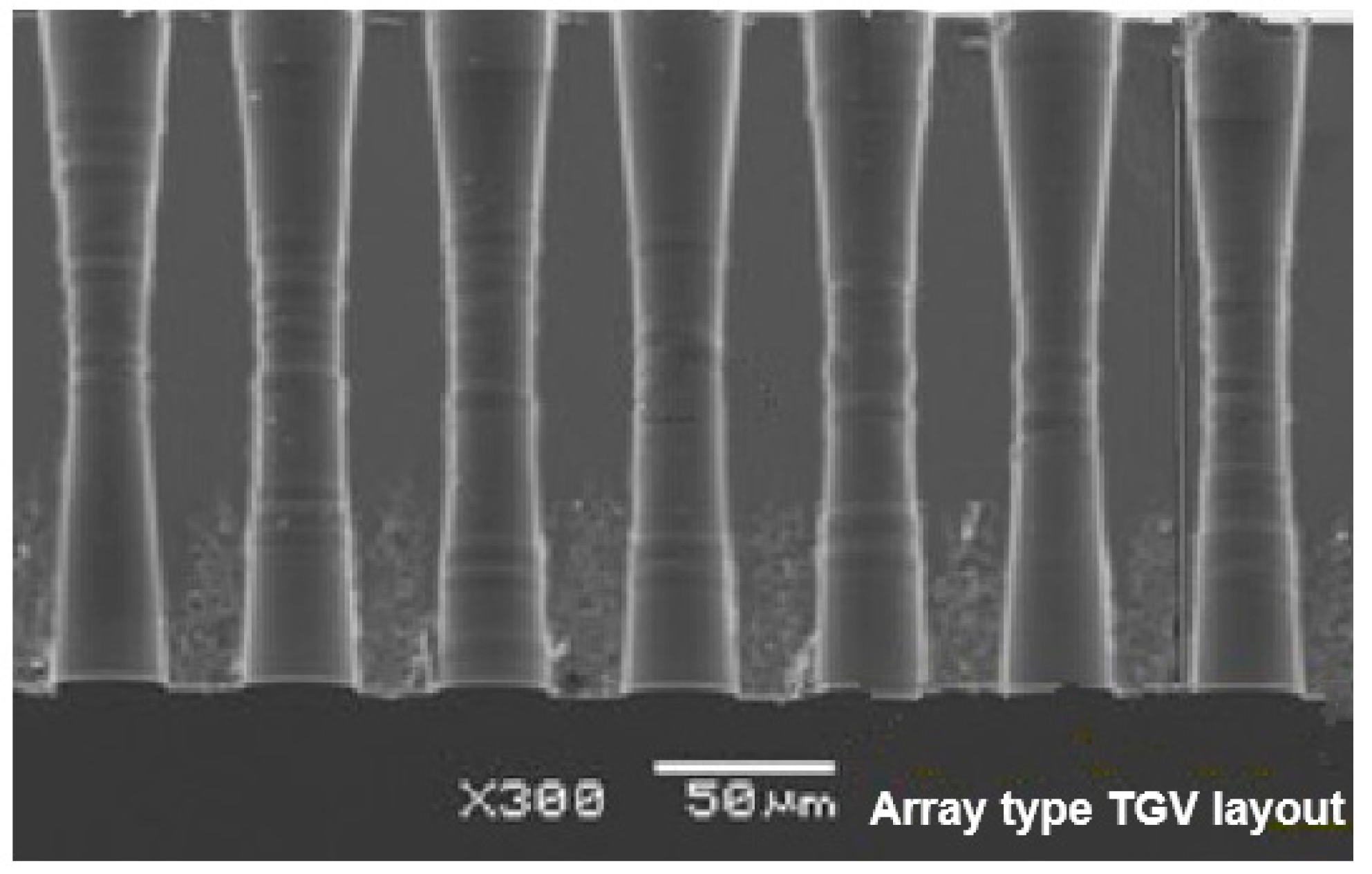
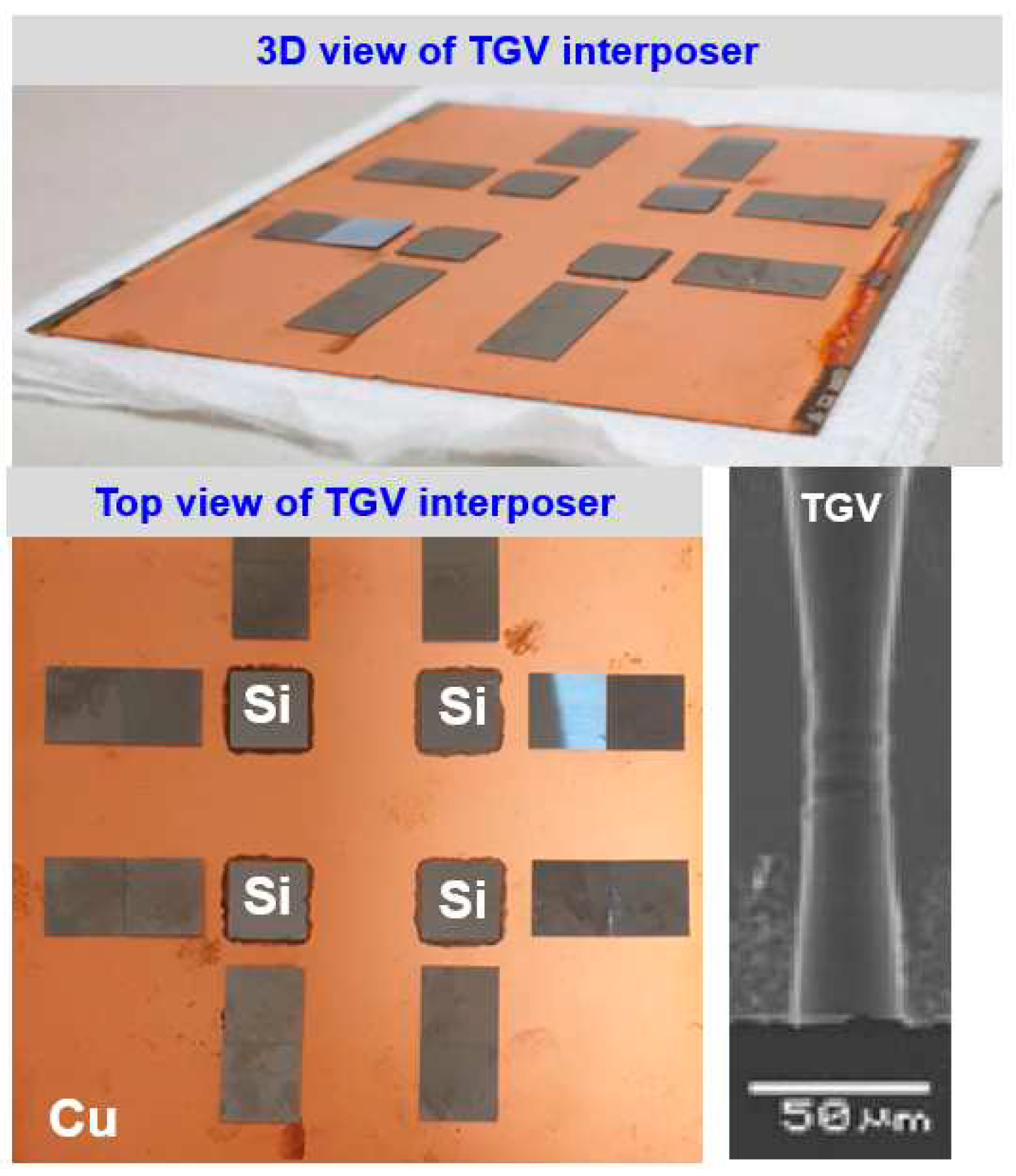
2. Structural layout design and fabrication process of glass interposer architecture with Cu-filled TGV array
3. Utilization of equivalent material approach and submodeling technique on stress generation mechanism estimation of glass interposer architecture with multi-chiplet arrangement
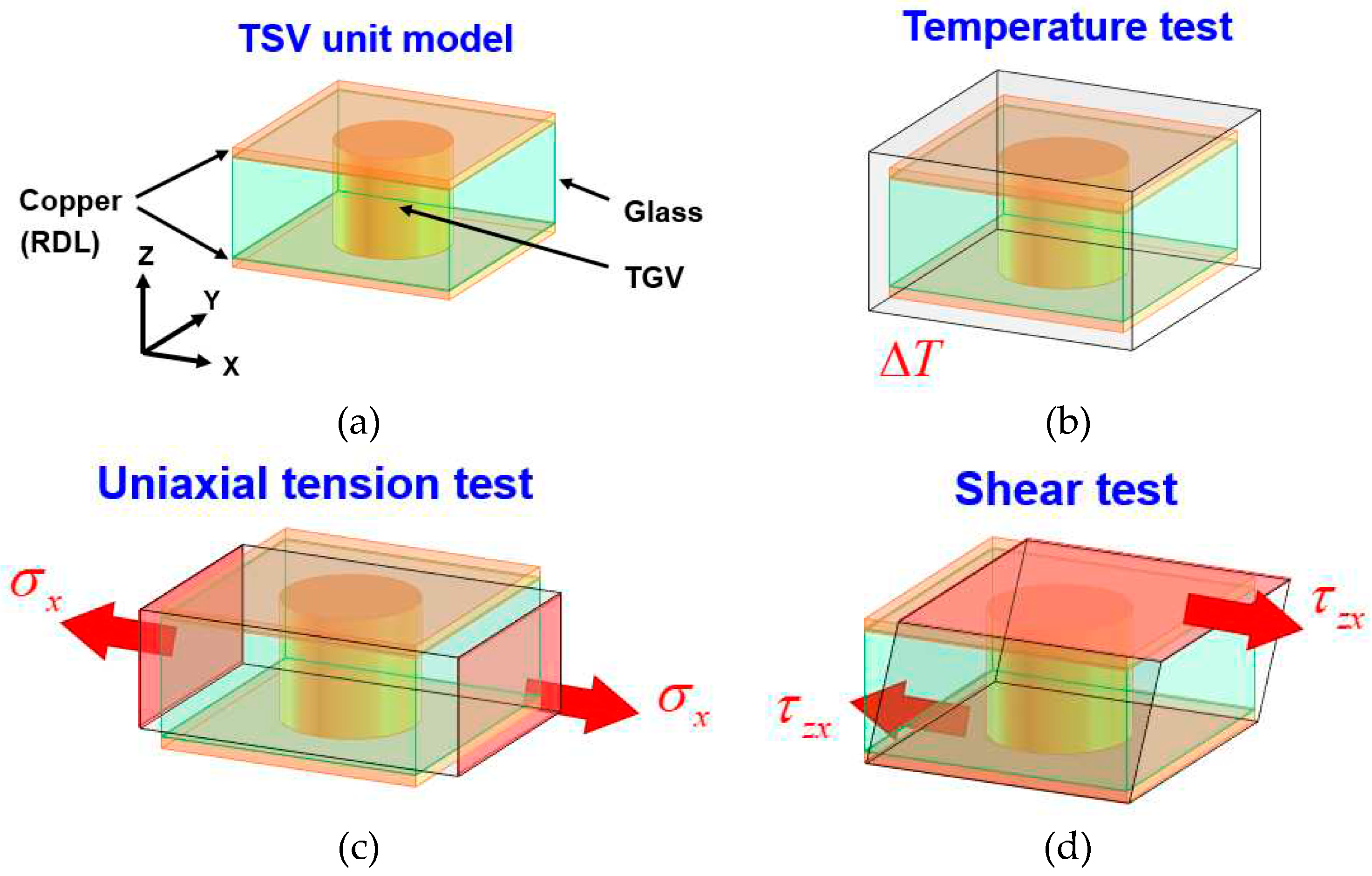
3.1. Equivalent material test approach for the equivalent mechanical property extraction of glass interposer with TGV array
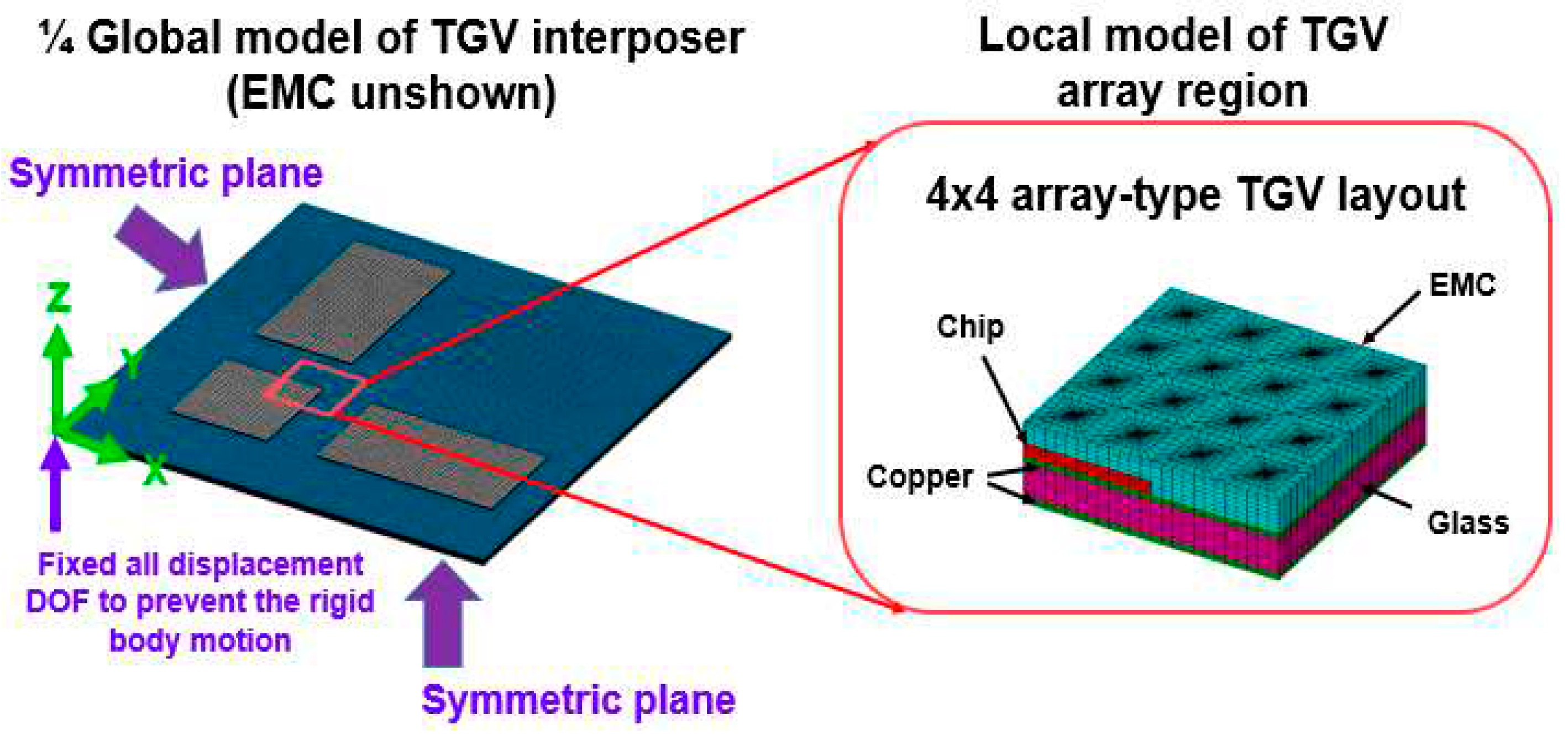
3.2. FEA modeling of glass interposer with multi-chiplet arrangement
3.3. Thermomechanical stress distribution and generation mechanism of glass interposer with multi-chiplet arrangement under the thermocompression process loading
3.4. Sensitivity analysis of different structural parameters of TGV array on stress generation of glass interposer
4. Results and discussion
4.1. Stress generation on glass interposer during high-temperature curing with various structural layout design parameters
4.2. Stress generation on glass interposer during cooling with various structural layout design parameters
5. Conclusions
Author Contributions
Funding
Data Availability Statement
Conflicts of Interest
References
- Sukumaran, V.; Bandyopadhyay, T.; Sundaram, V.; Tummala, R. Low-Cost Thin Glass Interposers as a Superior Alternative to Silicon and Organic Interposers for Packaging of 3-D ICs. IEEE Trans. Compon. Packag. Manuf. Technol. 2012, 2, 1426–1433. [Google Scholar] [CrossRef]
- El Amrani, A.; Benali, A. A Study of Through Package Vias in A Glass Interposer for Multifunctional and Miniaturized Systems. Microelectron. Reliab. 2014, 54, 1972–1976. [Google Scholar] [CrossRef]
- Ogutu, P.; Fey, E.; Borgesen, P.; Dimitrov, N. Hybrid Method for Metallization of Glass Interposers. N. Electrochem. Soc. 2013, 160, 3228–3236. [Google Scholar] [CrossRef]
- Woychik, C.; Lauffer, J.; Bajkowski, D.; Gaige, M.; Edwards, R.; Benninger, G.; Wilson, W. Processing Through Glass Via (TGV) Interposers for Advanced Packaging. In Proceedings of the International Symposium on Microelectronics, Pasadena, CA, USA, 8-11 October 2018; pp. 264–269. [Google Scholar]
- Nelson, S.F.; Levy, D.H.; Shorey, A.B. A Handling Solution for Easy Processing of Thin Glass with TGV. In Proceedings of the 2020 IEEE 70th Electronic Components and Technology Conference (ECTC), Orlando, FL, USA, 3-30 June 2020; pp. 1986–1991. [Google Scholar]
- Okoro, C.; Maurey, P.; Davis, R.; Pollard, S. Evaluation of the helium hermeticity reliability of copper through-glass vias. Microelectron. Reliab. 2022, 137, 114783. [Google Scholar] [CrossRef]
- Zhao, J.; Qin, F.; Yu, D.; Chen, Z.; Zhao, S. Warpage Characteristic of Glass Interposer with Different CTE’s and Thickness. In Proceedings of the 2021 22nd International Conference on Electronic Packaging Technology (ICEPT), Xiamen, China, 11–14 August 2021; pp. 1–4. [Google Scholar]
- Zhao, J.; Chen, Z.; Qin, F.; Yu, D. Thermo-Mechanical Reliability Study of Through Glass Vias in 3D Interconnection. Micromachines 2022, 13, 1799. [Google Scholar] [CrossRef] [PubMed]
- Santos, R.; Delrue, J.-P.; Ambrosius, N.; Ostholt, R.; Schmidt, S. Processing Glass Substrate for Advanced Packaging using Laser Induced Deep Etching. In Proceedings of the 2020 IEEE 70th Electronic Components and Technology Conference (ECTC), Orlando, FL, USA, 3-30 June 2020; pp. 1922–1927. [Google Scholar]
- Zhao, J.; Qin, F.; Yu, D.; Chen, Z. Reliability Study of WLP for IPD with Through Glass Vias Vertical Interconnection. In Proceedings of the 2022 23rd International Conference on Electronic Packaging Technology (ICEPT), Kuala Lumpur, Malaysia, 10-13 August 2022; pp. 1–4. [Google Scholar]
- Okoro, C.; Allowatt, T.; Pollard, S. Resolving Thermo-Mechanically Induced Circumferential Crack Formation in Copper Through-Glass Vias. In Proceedings of the 2021 IEEE 71st Electronic Components and Technology Conference (ECTC), San Diego, CA, USA, 1 June–4 July 2021; pp. 954–958. [Google Scholar]
- Okoro, C.; Maurey, P.; Pollard, S. Time and Temperature Dependence of Copper Protrusion in Metallized Through-Glass Vias (TGVs) Fabricated in Fused Silica Substrate. IEEE Trans. Device Mater. Reliab. 2021, 21, 129–136. [Google Scholar] [CrossRef]
- Okoro, C.; Jayaraman, S.; Pollard, S. Understanding and Eliminating Thermo-Mechanically Induced Radial Cracks in Fully Metallized Through-Glass Via (TGV) Substrates. Microelectron. Eng. 2021, 120, 114092. [Google Scholar] [CrossRef]
- Okoro, C.; Park, A.Y.; Allowatt, T.; Pollard, S. Elimination of Thermo-Mechanically Driven Circumferential Crack Formation in Copper Through-Glass via Substrate. IEEE Trans. Device Mater. Reliab. 2021, 21, 354–360. [Google Scholar] [CrossRef]
- Pan, K.; Xu, J.; Lai, Y.; Park, S.; Okoro, C.; Joshi, D.; Pollard, S. In-Situ Temperature-Dependent Characterization of Copper Through Glass Via (TGV). Microelectron. Eng. 2022, 129, 114487. [Google Scholar] [CrossRef]
- Pan, K.; Xu, J.; Park, S.; Okoro, C.; Joshi, D.; Pollard, S. Investigation of Copper and Glass Interaction in Through Glass Via (TGV) During Thermal Cycling. In Proceedings of the 2021 IEEE 71st Electronic Components and Technology Conference (ECTC), San Diego, CA, USA, 1 June–4 July 2021; pp. 1660–1666. [Google Scholar]
- Pan, K.; Okoro, C.; Lai, Y.; Joshi, C.; Park, S.; Pollard, S. A Comparative Study of The Thermomechanical Reliability of Fully-Filled and Conformal Through-Glass Via. In Proceedings of the 2022 IEEE 72nd Electronic Components and Technology Conference (ECTC), San Diego, CA, USA, 31 May–3 June 2022; pp. 1211–1217. [Google Scholar]
- Ahmed, O.; Jalilvand, G.; Pollard, S.; Okoro, C.; Jiang, T. The Interfacial Reliability of Through-Glass Vias for 2.5D Integrated Circuits. Microelectron. Int. 2020, 37, 181–188. [Google Scholar] [CrossRef]
- Okoro, C.; Jayaraman, S.; Pollard, S. Monitoring of the Effect of Thermal Shock on Crack Growth in Copper Through-Glass Via Substrates. In Proceedings of the 2021 IEEE 71st Electronic Components and Technology Conference (ECTC), San Diego, CA, USA, 1 June–4 July 2021; pp. 304–309. [Google Scholar]
- Benali, A.; Faqir, M.; Bouya, M.; Benabdellah, A.; Ghogho, M. Analytical and Finite Element Modeling of Through Glass Via Thermal Stress. Microelectron. Eng. 2016, 151, 12–18. [Google Scholar] [CrossRef]
- McCann, S.; Smet, V.; Sundaram, V.; Tummala, R.R.; Sitaraman, S.K. Experimental and Theoretical Assessment of Thin Glass Substrate for Low Warpage. IEEE Trans. Compon. Pack. Manuf. Technol. 2017, 7, 178–185. [Google Scholar] [CrossRef]
- Kuang, Y.; Xiao, D.; Zhou, J.; Li, W.; Hou, Z.; Chu, H.; Wu, X. Theoretical Model of Glass Reflow Process for Through Glass Via (TGV) Wafer Fabrication. J. Micromech. Microeng. 2018, 28, 095004. [Google Scholar] [CrossRef]
- Li, W.; Xing, C.; Zhang, J.; Wang, Z.; Su, Z.; Luo, B.; Shang, J. Glass Reflow and Thermo-Mechanical Stress Simulation for Through Glass Via in Glass-Silicon Composite Interposer. In Proceedings of the 2021 22nd International Conference on Electronic Packaging Technology (ICEPT), Xiamen, China, 11–14 August 2021; pp. 1–4. [Google Scholar]
- Yu, W.; Yang, S.Y.P.; Glancey, C.; Ong, Y.C.; Ng, H.W. Package Warpage Modeling by Considering Shrinkage Behavior of EMC and Substrate. In Proceedings of the 2021 IEEE 23rd Electronics Packaging Technology Conference (EPTC), Singapore, Singapore, 7–9 December 2021; pp. 547–552. [Google Scholar]
- Che, F.X.; Ho, D.; Chai, T.C. Study on Warpage and Reliability of Fan-Out Interposer Technology. IEEE Trans. Compon. Pack. Manuf. Technol. 2019, 9, 786–796. [Google Scholar] [CrossRef]
- Shih, M.; Chen, K.; Lee, T.; Tarng, D.; Hung, C.P. FE Simulation Model for Warpage Evaluation of Glass Interposer Substrate Packages. IEEE Trans. Compon. Packag. Manuf. Technol. 2021, 11, 690–696. [Google Scholar] [CrossRef]
- Burd, T.; Beck, N.; White, S.; Paraschou, M.; Kalyanasundharam, N.; Donley, G.; Smith, A.; Hewitt, L.; Naffziger, S. Zeppelin: An SoC for multichip architectures. IEEE J. Solid-State Circuits 2019, 54, 133–143. [Google Scholar] [CrossRef]
- Greenhill, D.; Ho, R.; Lewis, D.; Schmit, H.; Chan, K.H.; Tong, A.; Atsatt, S.; How, D.; McElheny, P.; Duwel, K.; Schulz, J.; Faulkner, D.; Iyer, G.; Chen, G.; Phoon, H.K.; Lim, H.W.; Koay, W.Y.; Garibay, T. A 14nm 1GHz FPGA with 2. 5D Transceiver Integration. In Proceedings of the 2017 IEEE International Solid-State Circuits Conference (ISSCC), San Francisco, CA, USA, 5–9 February 2017; pp. 54–56. [Google Scholar]
- Lin, M.S.; Huang, T.C.; Tsai, C.C.; Tam, K.H.; Hsieh, C.H.; Chen, T.; Huang, W.H.; Hu, J.; Chen, Y.C.; Goel, S.K.; et al. A 7 nm 4 GHz Arm1-Core-Based CoWoS1 Chiplet Design for High Performance Computing. In Proceedings of the 2019 Symposium on VLSI Circuits, Kyoto, Japan, 9–14 June 2019; pp. C28–C29. [Google Scholar]
- Li, T.; Hou, J.; Yan, J.; Liu, R.; Yang, H.; Sun, Z. Chiplet Heterogeneous Integration Technology—Status and Challenges. Electronics 2020, 9, 670. [Google Scholar] [CrossRef]
- Ahmad, M.; DeLaCruz, J.; Ramamurthy, A. Heterogeneous Integration of Chiplets: Cost and Yield Tradeoff Analysis. In Proceedings of the 2022 International Conference on Thermal, Mechanical and Multi-Physics Simulation and Experiments in Microelectronics and Microsystems, St Julian, Malta, 25-27 April 2022; pp. 1–9. [Google Scholar]
- Chiang, Y.P.; Tai, S.P.; Wu, W.C.; Yeh, J.; Wang, C.T.; Yu, D.C.H. InFO_oS (Integrated Fan-Out on Substrate) Technology for Advanced Chiplet Integration. In Proceedings of the 2021 IEEE 71st Electronic Components and Technology Conference, San Diego, CA, USA, 1 June 2021-4 July 2021; pp. 130–135. [Google Scholar]
- Shan, G.; Zheng, Y.; Xing, C.; Chen, D.; Li, G.; Yang, Y. Architecture of Computing System Based on Chiplet. Micromachines 2022, 13, 205. [Google Scholar] [CrossRef] [PubMed]
- Lin, Y.; Yew, M.C.; Chen, S.M.; Liu, M.S.; Kavle, P.; Lai, T.M.; Yu, C.T.; Hsu, F.C.; Chen, C.S.; Fang, T.J.; Chen, C.S.; Yu, C.T.; Lee, K.C.; Hsu, C.K.; Lin, P.Y.; Hsu, F.C.; Jeng, S.P. Multilayer RDL Interposer for Heterogeneous Device and Module Integration. In Proceedings of the 2019 IEEE 69th Electronic Components and Technology Conference, Las Vegas, NV, USA, 28–31 May 2019; pp. 931–936. [Google Scholar]
- Wong, J.H.; Wu, N.Y.; Lai, W.H.; Chen, D.L.; Chen, T.Y.; Chen, C.H.; Wu, Y.H.; Chang, Y.S.; Kao, C.L.; Tarng, D.; Lee, T.C.; Hung, C.P. Warpage and RDL Stress Analysis in Large Fan-Out Package with Multi-Chiplet Integration. In Proceedings of the 2022 IEEE 72nd Electronic Components and Technology Conference, San Diego, CA, USA, 31 May 2022-3 June 2022; pp. 1074–1079. [Google Scholar]
- Ravichandran, S.; Kathaperumal, M.; Swaminathan, M.; Tummala, R. Large-body-sized Glass-based Active Interposer for High-Performance Computing. In Proceedings of the 2020 IEEE 70th Electronic Components and Technology Conference, Orlando, FL, USA, 3 June 2020-30 June 2020; pp. 879–884. [Google Scholar]
- Kudo, H.; Takano, T.; Akazawa, M.; Yamada, S.; Sakamoto, K.; Kitayama, D.; Iida, H.; Tanaka, M.; Tai, T. High-Speed, High-Density, and Highly-Manufacturable Cu-filled Through-Glass-Via Channel (Cu bridge) for Multi-Chiplet Systems. In Proceedings of the 2021 IEEE 71st Electronic Components and Technology Conference (ECTC), San Diego, CA, USA, 1 June–4 July 2021; pp. 1031–1037. [Google Scholar]
- Wang, S.H.; Hsu, W.; Liou, Y.Y.; Huang, P.C.; Lee, C.C. Reliability Assessment of Thermocompressed Epoxy Molding Compound through Glass via Interposer Architecture by the Submodeling Simulation Approach. Materials 2022, 15, 7357. [Google Scholar] [CrossRef] [PubMed]

Disclaimer/Publisher’s Note: The statements, opinions and data contained in all publications are solely those of the individual author(s) and contributor(s) and not of MDPI and/or the editor(s). MDPI and/or the editor(s) disclaim responsibility for any injury to people or property resulting from any ideas, methods, instructions or products referred to in the content. |
© 2023 by the authors. Licensee MDPI, Basel, Switzerland. This article is an open access article distributed under the terms and conditions of the Creative Commons Attribution (CC BY) license (http://creativecommons.org/licenses/by/4.0/).


