1. Introduction
Coating from the solution phase is one of the key technologies for processing of organic semiconductors, a technology featuring low energy consumption and low production cost. In the following we will focus on the materials class of conjugated molecules, such as TIPS-pn (6,13-bis(triisopropyl silanyl ethynyl) pentacene), diF-TES-ADT (2,8-difluoro 5,11-bis( triethylene silanyl ethynyl) anthradithiophene), or C8-BTBT (2,7-dioctyl benzothienobenzothiophene) which have recently been shown to display high charge mobilities, while being processed from solution at low temperatures between 50-100°C. The charge carrier mobility in a molecular organic semiconductor is determined by the intrinsic, highly anisotropic mobility inside a single-crystalline grain and the grain boundaries that the charge carriers have to pass. Recently a number of publications have reported directional growth of long needles which would eliminate grain boundaries from the charge carrier path[
1,
2,
3,
4,
5,
6,
7]. Such studies shall be reviewed in the following sections and a suggestion for the growth mechanism shall be given.
2. Coating Processes
Common to all deposition processes of conjugated molecules is that often there is a preferential crystallographic plane that grows parallel to the substrate surface while laterally the grains have either random orientation (so-called 2D powders) or a certain degree of directionality that depends on details of the deposition process.
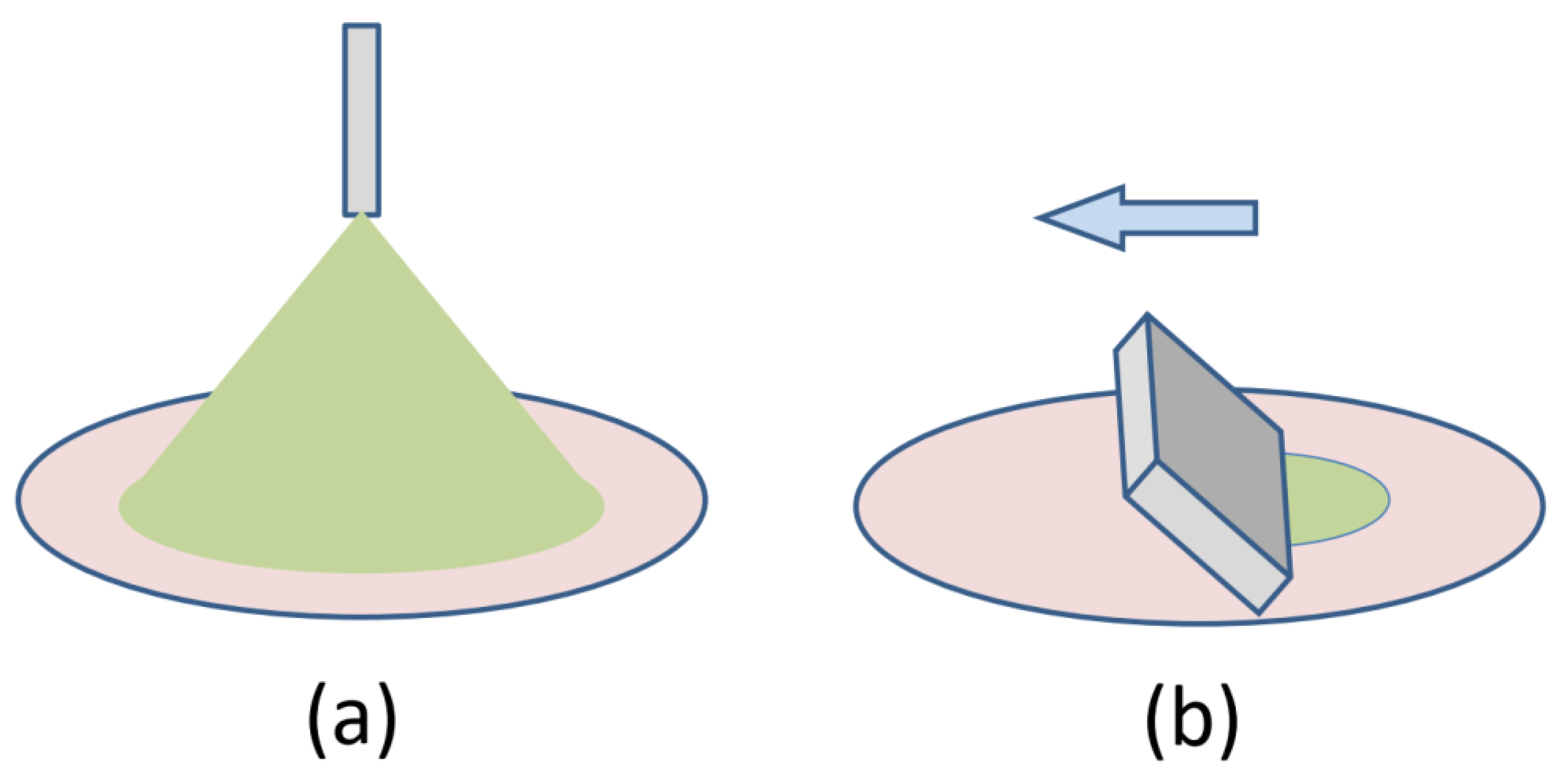
Coating processes can be classified into isotropic and directional. Isotropic growth i.e. arbitrary lateral grain orientation, has been observed in drop casting, spray coating, and for the most part in spin coating. In directional coating processes mechanical devices or drying geometry impose that a straight drying line sweeps across the substrate. The most sophisticated coating technique of this class is premetered slot-die coating. Here the amount of material going into the slot-die head and the amount of material deposited on the substrate are precisely controlled, an important factor when coating costly designer molecules with typical prices of $1,000 per gram. A simpler method is self-metered knife coating, also referred to as blade coating, doctor blading, or shear coating, with some variation in the details. Finally there is pen writing and dip coating where the solution is deposited by capillary action. In the following we will focus on such directional coating processes.
Figure 1.
Classification of coating processes. (a) Isotropic coating such as drop casting, spray coating (shown) and spin coating result in a random lateral orientation of grains on the substrate. (b) Directional coating, such as slot-die coating, blade coating (shown), or dip coating can result in a preferential lateral orientation, as discussed in the text.
Directional coating is a non-equilibrium process involving multiple length and time scales. When the solution leaves the coating device it thins within the meniscus region from the coating gap of typically 100 to 500 µm to about a tenth of this value at the end of the meniscus – this stage can be understood by the hydrodynamic interplay of viscosity and surface tension. The next stage is evaporation which starts as soon as the solution leaves the coating device until the solute solidifies. Typically, conjugated molecules are dissolved at concentrations around 10 mg/mL which corresponds to a volume ratio of solvent to solute of about 100:1. Hence the film thins by another factor of 100 due to evaporation of the solvent. The goal for the deposition is to achieve film thicknesses of 50 to 100 nm which constitutes a compromise between reliability and cost efficiency, with the channel width of a field-effect transistor being typically 30 nm.
It is a matter of the coating regime whether deposition and evaporation concur simultaneously or can be considered as two independent steps. In the former case, the evaporation regime, the film solidifies at the edge of the meniscus. Here film thickness
h scales with coating speed
v as
v-1 [
8]. At faster coating speed, the final film thickness is determined by the hydrodynamic boundary layer thickness, the well-known Landau-Levich regime, in which
h scales as
v2/3 [
8,
9]. In this regime a thin liquid film is coated. The transition between the two regimes occurs at coating speeds on the order of 1 mm/s where the film thickness assumes a minimum. Directional crystallization is typically observed in this transition regime [
10].
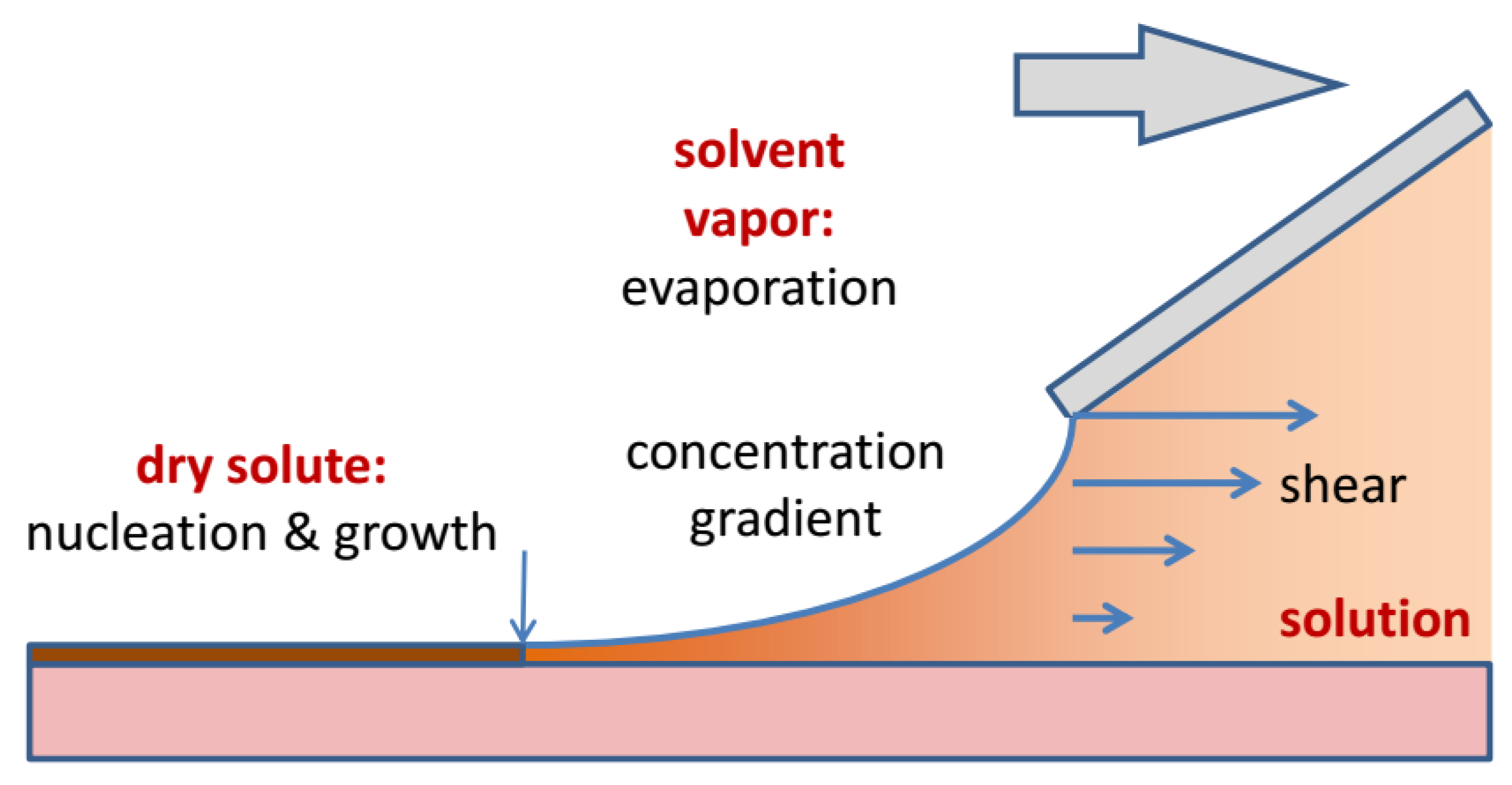
Figure 2.
Processes during knife coating. At the edge of the coating blade a well-defined shear field forms in the solution. As soon as the solution leaves the reservoir under the coating blade, evaporation sets in. Eventually the supersaturation of the solution is high enough that solidification sets in at the drying line (arrow). Convective Marangoni currents may transport additional molecules to the drying line.
Looking at the meniscus region in more detail, it becomes clear that coating is a complex non-equilibrium process. As the solution leaves the slot-die or the coating blade there is a well-defined shear field with a shear rate given by γ = v/h. In the meniscus region the velocity gradient and hence the shear gradient diminishes, until the whole liquid column moves with the substrate speed. Evaporation of the solvent creates a concentration gradient perpendicular to the meniscus. Solidification at the drying line depletes the concentration of the solute in the solution and thus creates a concentration gradient at the drying line. This gradient will induce diffusive and convective transport of solute to the drying line. When the solution reaches the critical supersaturation nucleation will occur, either at the film-substrate interface, at the film surface, or both. Finally, the solution concentration, the volatility of the solvent and the temperature of the substrate will determine how fast solvent evaporation and solute crystallization will occur.
Opinions on the role of shear during coating differ in literature [
6,
7,
11,
12,
13,
14,
15,
16]. In order to shed light onto the importance of shear for directional crystallization we reviewed a number of recent publications in which directional crystallization was achieved with a variety of coating methods and different amounts of shear exerted. Chang et al. reported directional crystallization in slot-die coating using coating speeds between 0.2 and 1 mm/s and coating gaps between 10 µm to 90 µm [
17]. In our own work based on knife coating [
10] we observed directional crystallization between 0.4 and 1 mm/s using a coating gap of 100 µm. In our experiments we have found that a small coating gap in the range of 100 to 200 µm makes the meniscus more stable with regard to vibrations and thus facilitates a more homogeneous deposit. Headrick and coworkers achieved directional crystallization using a hollow pen writer at a speed of 0.1 mm/s and a large coating gap of 0.6 mm [
18]. Directional growth was also reported during dipcoating by Chang and coworkers [
17]. Coating speed was here 0.7 mm/s and no mechanical barrier limited the initial film thickness. A similar result was obtained by Zhang et al. who also studied different angles to withdraw the substrate from the solution [
19]. Interestingly Lee et al. as well as Rivnay et al. obtained directional crystallization even in simple dropcasting on a substrate inclined by 2° [
20,
21]. In this case, surface tension prevented the solution drop from running off the substrate, while gravity gave rise to a wedge-shaped liquid layer. Without any mechanical action, the drying line moved slowly across the substrate.
Hence it appears that directional crystallization is an effect of the speed of the drying line, but independent of shear rate, since we find that results are essentially independent of the coating gap. Indeed, rotational diffusion in small molecules is too fast to maintain any degree of orientation induced by the shear field at the coating blade by the time the drying line is reached. In contrast conjugated polymers may retain some shear memory, in particular for higher molecular weights.
3. A Hartman-Perdok picture of coating
In order to rationalize why directional crystallization seems to be a matter of the speed at which the drying line sweeps across the substrate, we take a look at classic Hartman-Perdok theory [
22,
23]. Hartman and Perdok were interested in which crystallographic planes are expressed for a macroscopic single crystal, i.e. the crystal habit. They concluded that stable facets are produced by the planes of slowest growth. These are typically the low-index Miller planes which feature smooth surfaces and a low density of docking sites. In contrast vicinal surfaces have steps and kinks and display a much higher density of docking sites and grow faster; hence such planes are not found in the habit of the crystal.
In the case of a moving drying line we have the reverse situation: only planes with the fastest growing speed can follow the drying line, and such crystallites will grow in a specific direction. Other growth planes may form temporarily, but cannot keep up with the moving drying line and are cut off from further material transport. Thus, the drying line speed serves as a filter, allowing only the fastest growing planes to grow further. At lower coating speeds, multiple crystallographic planes can grow simultaneously, and eventually a 2D powder is formed with a random grain orientation. In the Landau-Levich regime at high coating speeds, nucleation occurs at random sites in the liquid film, often in the form of fast-growing spherulites, and again a 2D powder is formed. Hence there is only a small window of coating speeds where directional crystallization can occur.
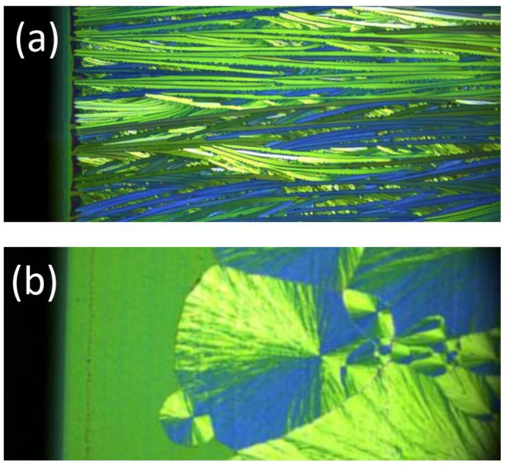
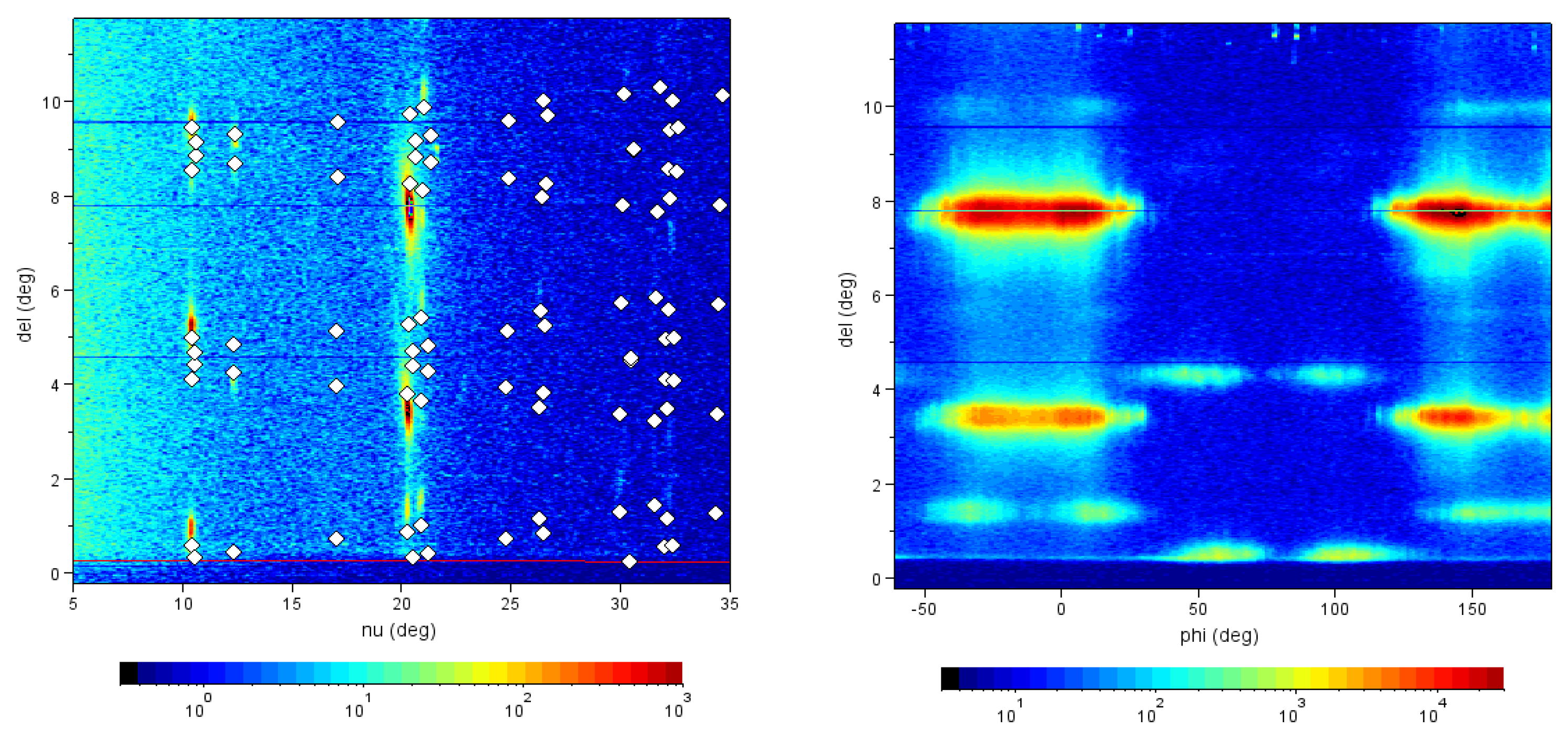
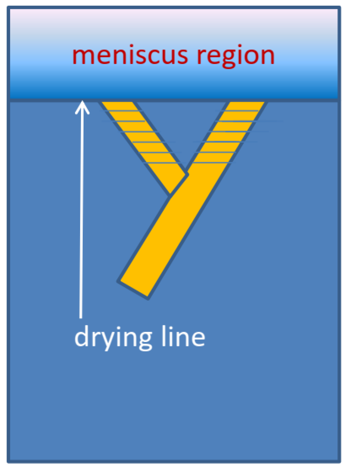
If nucleation is high enough, multiple needle-like crystallites can form at the drying line. The sides of the needles will usually feature relatively stable slow-growing low-index planes. In low-symmetry triclinic or monoclinic lattices which are typically found for conjugated molecules, the growth front and the sides of the needles do not have to be perpendicular. Such a situation can give rise to twinning and the growth results in two needle orientations, as shown in
Figure 3a. Such a behavior was beautifully confirmed in high-resolution diffraction images taken at G2 station (see
Figure 4) using a six-circle diffractometer with a high-resolution Soller slit and a linear diode array detector which simultaneously records the scattering intensity over a range of exit angles from the sample surface [
27]. Our proposed twinning mechanism is illustrated in
Figure 5.
4. Synchronizing clocks
In our experiments a variety of conjugated molecules and solvents at different concentrations was used as well as various substrate temperatures and coating speeds. The substrate temperature controls the rate of evaporation as well as the diffusion rate to the drying line and the crystallization kinetics. The coating speed needs to be chosen properly so that the molecules can still attach to a growing crystal at the edge of the meniscus. Another factor is the initial concentration of the solute which determines when oversaturation is reached at a given substrate temperature as well as materials properties of solute, solvent, and their combination. Hence achieving a high-quality directional crystallization seems to be a matter of synchronizing the different time scales involved, as defined by the coating speed, the crystallization speed, and the mass transport to the drying line. If the coating speed is too slow, multiple crystallites can grow and selectivity is lost [
10]. If the coating speed is too fast, an intermediate liquid or amorphous film appears which subsequently nucleates spontaneously forming spherulites [
3,
28] Again the directionality is lost. Fortuitously the island of opportunity is not too sharply defined. A good guide is to look for the transition regime of film thickness versus coating speed. Thus the experimenter has a good chance of locating the directional crystallization regime and then finetuning the coating parameters to achieve optimal performance.
5. Conclusion
Directional crystallization is an attractive way of optimizing charge mobility in organic field-effect transistors [
1,
2,
4,
5,
6,
29,
30]. We have shown here that directional crystallization occurs for a variety of coating techniques. We explain our findings by invoking classical crystallization theory and observing that under proper conditions only the fastest growth planes can follow the drying line. Due to the low symmetry lattices of most molecules, twinning is still possible which may limit the attainable length of single crystalline domains.
Author Contributions
Conceptualization, D.-M.S. and R.L.; methodology, D.-M.S. and R.L.; investigation, D.-M.S. and R.L.; writing—original draft preparation, D.-M.S.; writing—review and editing, D.-M.S. and R.L. All authors have read and agreed to the published version of the manuscript.
Funding
Part of this work was performed at the Cornell high Energy Synchrotron Source which was funded by the National Science Foundation via award DMR—1332208.
Data Availability Statement
The data presented in this study are available from the authors upon reasonable request.
Acknowledgments
We thank Gaurav Giri and Zhenan Bao (Stanford University) as well as Aram Amassian (King Abdullah University of Science and Technology, Saudi Arabia), Randy Headrick (University of Vermont) and Lee Richter (National Institute of Science and Technology) for stimulating discussions on coating.
Conflicts of Interest
The authors declare no conflict of interest.
References
- Niazi, M.R.; Li, R.; Abdelsamie, M.; Zhao, K.; Anjum, D.H.; Payne, M.M.; Anthony, J.; Smilgies, D.M.; Amassian, A. Contact-Induced Nucleation in High-Performance Bottom-Contact Organic Thin Film Transistors Manufactured by Large-Area Compatible Solution Processing. Adv Funct Mater 2016, 26, 2371–2378. [Google Scholar] [CrossRef]
- Diao, Y.; Shaw, L.; Bao, Z.; Mannsfeld, S.C.B. Morphology Control Strategies for Solution-Processed Organic Semiconductor Thin Films. Energy Environ Sci 2014, 7, 2145–2159. [Google Scholar] [CrossRef]
- Lee, S.S.; Loth, M.A.; Anthony, J.E.; Loo, Y.L. Orientation-Independent Charge Transport in Single Spherulites from Solution-Processed Organic Semiconductors. J Am Chem Soc 2012, 134, 5436–5439. [Google Scholar] [CrossRef] [PubMed]
- Gu, X.; Shaw, L.; Gu, K.; Toney, M.F.; Bao, Z. The Meniscus-Guided Deposition of Semiconducting Polymers. Nat Commun 2018, 9, 534. [Google Scholar] [CrossRef] [PubMed]
- Lu, Z.; Wang, C.; Deng, W.; Achille, M.T.; Jie, J.; Zhang, X. Meniscus-Guided Coating of Organic Crystalline Thin Films for High-Performance Organic Field-Effect Transistors. J Mater Chem C Mater 2020, 8, 9133–9146. [Google Scholar] [CrossRef]
- Chen, M.; Peng, B.; Huang, S.; Chan, P.K.L. Understanding the Meniscus-Guided Coating Parameters in Organic Field-Effect-Transistor Fabrications. Adv Funct Mater 2020, 30, 1905963. [Google Scholar] [CrossRef]
- Yildiz, O.; Wang, Z.; Borkowski, M.; Fytas, G.; Blom, P.W.M.; Michels, J.J.; Pisula, W.; Marszalek, T. Optimized Charge Transport in Molecular Semiconductors by Control of Fluid Dynamics and Crystallization in Meniscus-Guided Coating. Adv Funct Mater 2022, 32, 2107976. [Google Scholar] [CrossRef]
- Le Berre, M.; Chen, Y.; Baigl, D. From Convective Assembly to Landau - Levich Deposition of Multilayered Phospholipid Films of Controlled Thickness. Langmuir 2009, 25, 2554–2557. [Google Scholar] [CrossRef]
- Landau, L.D.; Levich, B. Dragging of a Liquid by a Moving Plate. Acta Physicochimica U.R.S.S. 1942, 17, 42–54. [Google Scholar] [CrossRef]
- Smilgies, D.M.; Li, R.; Giri, G.; Chou, K.W.; Diao, Y.; Bao, Z.; Amassian, A. Look Fast: Crystallization of Conjugated Molecules during Solution Shearing Probed in-Situ and in Real Time by X-Ray Scattering. Physica Status Solidi - Rap Res Lett 2013, 7, 177–179. [Google Scholar] [CrossRef]
- Becerril, H.A.; Roberts, M.E.; Liu, Z.; Locklin, J.; Bao, Z. High-Performance Organic Thin-Film Transistors through Solution-Sheared Deposition of Small-Molecule Organic Semiconductors. Adv Mater 2008, 20, 2588–2594. [Google Scholar] [CrossRef]
- Diao, Y.; Tee, B.C.K.; Giri, G.; Xu, J.; Kim, D.H.; Becerril, H.A.; Stoltenberg, R.M.; Lee, T.H.; Xue, G.; Mannsfeld, S.C.B.; et al. Solution Coating of Large-Area Organic Semiconductor Thin Films with Aligned Single-Crystalline Domains. Nat Mater 2013, 12, 665–671. [Google Scholar] [CrossRef]
- Giri, G.; Verploegen, E.; Mannsfeld, S.C.B.; Atahan-Evrenk, S.; Kim, D.H.; Lee, S.Y.; Becerril, H.A.; Aspuru-Guzik, A.; Toney, M.F.; Bao, Z. Tuning Charge Transport in Solution-Sheared Organic Semiconductors Using Lattice Strain. Nature 2011, 480, 504–508. [Google Scholar] [CrossRef]
- Giri, G.; Li, R.; Smilgies, D.M.; Li, E.Q.; Diao, Y.; Lenn, K.M.; Chiu, M.; Lin, D.W.; Allen, R.; Reinspach, J.; et al. One-Dimensional Self-Confinement Promotes Polymorph Selection in Large-Area Organic Semiconductor Thin Films. Nat Commun 2014, 5, 3573. [Google Scholar] [CrossRef]
- Li, Y.; Wan, J.; Smilgies, D.M.; Bouffard, N.; Sun, R.; Headrick, R.L. Nucleation and Strain-Stabilization during Organic Semiconductor Thin Film Deposition. Sci Rep 2016, 6, 32620. [Google Scholar] [CrossRef]
- Richter, L.J.; Delongchamp, D.M.; Amassian, A. Morphology Development in Solution-Processed Functional Organic Blend Films: An in Situ Viewpoint. Chem Rev 2017, 117, 6332–6366. [Google Scholar] [CrossRef] [PubMed]
- Chang, J.; Chi, C.; Zhang, J.; Wu, J. Controlled Growth of Large-Area High-Performance Small-Molecule Organic Single-Crystalline Transistors by Slot-Die Coating Using a Mixed Solvent System. Advanced Materials 2013, 25, 6442–6447. [Google Scholar] [CrossRef] [PubMed]
- Wo, S.; Headrick, R.L.; Anthony, J.E. Fabrication and Characterization of Controllable Grain Boundary Arrays in Solution-Processed Small Molecule Organic Semiconductor Films. J Appl Phys 2012, 111. [Google Scholar] [CrossRef]
- Zhang, K.; Wang, Z.; Marszalek, T.; Borkowski, M.; Fytas, G.; Blom, P.W.M.; Pisula, W. Key Role of the Meniscus Shape in Crystallization of Organic Semiconductors during Meniscus-Guided Coating. Mater Horiz 2020, 7, 1631–1640. [Google Scholar] [CrossRef]
- Lee, W.H.; Kim, D.H.; Jang, Y.; Cho, J.H.; Hwang, M.; Park, Y.D.; Kim, Y.H.; Han, J.I.; Cho, K. Solution-Processable Pentacene Microcrystal Arrays for High Performance Organic Field-Effect Transistors. Appl Phys Lett 2007, 90, 132106. [Google Scholar] [CrossRef]
- Rivnay, J.; Jimison, L.H.; Northrup, J.E.; Toney, M.F.; Noriega, R.; Lu, S.; Marks, T.J.; Facchetti, A.; Salleo, A. Large Modulation of Carrier Transport by Grain-Boundary Molecular Packing and Microstructure in Organic Thin Films. Nat Mater 2009, 8, 952–958. [Google Scholar] [CrossRef]
- Hartman, P.; Perdok, W.G. On the Relations Between Structure and Morphology of Crystals. I. Acta Cryst 1955, 8, 49–52. [Google Scholar] [CrossRef]
- Hartman, P.; Perdok, W.G. On the Relations Between Structure and Morphology of Crystals. II. Acta Cryst 1955, 8, 521–524. [Google Scholar] [CrossRef]
- Smilgies, D.M.; Blasini, D.R. Indexation Scheme for Oriented Molecular Thin Films Studied with Grazing-Incidence Reciprocal-Space Mapping. J Appl Crystallogr 2007, 40, 716–718. [Google Scholar] [CrossRef]
- Smilgies, D.-M.; Li, R. IndexGIXS-Software for Visualizing and Interactive Indexing of Grazing-Incidence Scattering Data. ChemRxiv 2022. [Google Scholar] [CrossRef]
- Jurchescu, O.D.; Mourey, D.A.; Subramanian, S.; Parkin, S.R.; Vogel, B.M.; Anthony, J.E.; Jackson, T.N.; Gundlach, D.J. Effects of Polymorphism on Charge Transport in Organic Semiconductors. Phys Rev B 2009, 80, 085201. [Google Scholar] [CrossRef]
- Smilgies, D.M.; Blasini, D.R.; Hotta, S.; Yanagi, H. Reciprocal Space Mapping and Single-Crystal Scattering Rods. J Synchrotron Rad 2005, 12, 807–811. [Google Scholar] [CrossRef] [PubMed]
- Wan, J.; Li, Y.; Ulbrandt, J.G.; Smilgies, D.M.; Hollin, J.; Whalley, A.C.; Headrick, R.L. Transient Phases during Fast Crystallization of Organic Thin Films from Solution. APL Mater 2016, 4, 016103. [Google Scholar] [CrossRef]
- Riera-Galindo, S.; Tamayo, A.; Mas-Torrent, M. Role of Polymorphism and Thin-Film Morphology in Organic Semiconductors Processed by Solution Shearing. ACS Omega 2018, 3, 2329–2339. [Google Scholar] [CrossRef]
- Zhao, H.; Wang, Z.; Dong, G.; Duan, L. Fabrication of Highly Oriented Large-Scale TIPS Pentacene Crystals and Transistors by the Marangoni Effect-Controlled Growth Method. Physical Chemistry Chemical Physics 2015, 17, 6274–6279. [Google Scholar] [CrossRef]
|
Disclaimer/Publisher’s Note: The statements, opinions and data contained in all publications are solely those of the individual author(s) and contributor(s) and not of MDPI and/or the editor(s). MDPI and/or the editor(s) disclaim responsibility for any injury to people or property resulting from any ideas, methods, instructions or products referred to in the content. |
© 2023 by the authors. Licensee MDPI, Basel, Switzerland. This article is an open access article distributed under the terms and conditions of the Creative Commons Attribution (CC BY) license (http://creativecommons.org/licenses/by/4.0/).
