1. Introduction
The reliability issue for electronic systems is gaining more attention because of advancement and scaling down of technology nodes. Continuous device shrinking, increased integration level, extremely low operating voltage, structural changes, high speeds etc. have caused semiconductor or other related devices 2D devices to be more sensitive to radiation, consequently leading to electronic system failures and mal function. Hence, the need to investigate radiation and its impacts on the reliability of VLSI design.
SRAM is an essential building block of a memory unit, which is usually designed for high speed and low power applications. It is characterized with high integration capability, fast storage speed and compatible with CMOS. In a radiation environment such as space, radiation particle (e.g., alpha particles, protons, neutrons, or other heavy ions) causes a decrease in critical charge and capacitance of SRAM, thus more susceptible to Single Event Upset (SEU) [
1]. An electron-hole pair is generated along the path of a charged particle in a semiconductor device, which results in collected charge (Q
coll). The Q
coll can change the state of register, latch, memory cell or flip flops, if it exceeds the threshold value, critical charge (Q
crit). Several research have been conducted to investigate the soft error caused by radiation effect. Li et al. and Mahyuddin et al. introduced a strike at the circuit node with a transient current source to emulate SEU [
2]. Similarly, the SEU effect in III-V Hetero-junction TFET, III-V FinFET and Si FinFET are investigated using circuit simulation [
3]. The soft error performance before and after radiation in DG TFETs 6T SRAM cell are also studied. Xiang et al. showed the effect of single event transient (SET) in a phase locked loop and proposed SET-hardened structure to improve the irradiation resistance of PLL [
4,
5]. Note that it has been shown theoretically and experimentally that graphene nano-ribbon FET (GNRFET) can potentially replace planar CMOS and FinFET [
6]. GNR has a finite band gap with good semiconductor properties, GNR transistor exhibits low sub-threshold swing and high on/off ratio, which makes it suitable for logic and low power applications. A brief review and analyses of GNRFET will be discussed later in this work.
In this paper, we present device level characteristics of GNRFET, study and compare SRAM circuits made of MOS-GNRFETs and FinFETs and investigate their soft error performance.
2. GNRFET Device Simulation and Characterization
Graphene nanoribbon (GNR) FET are made from GNRs which are 1D nano-sized graphite layers or strips of graphene with superlative electronic properties. Graphene, in its pristine condition, has no bandgap and causes poor on/off current ratio and subthreshold, thus it is not suitable for digital applications. However, its width can be patterned and modified to a few nanometers 1D GNR, thereby creating a finite gap which is required for a semiconductor. The width of GNR is inversely proportional to induced bandgap, GNRFET switch-ability can be improved by increasing the width of the nanoribbon. Certain variability and defects can emerge from oxide thickness, GNR width, line of edge roughness (LER) that affect the performance of GNRFET. The different planar structure and models of MOS-GNRFET and SB-GNRFET are already presented in ref.[
7], we have chosen MOS-GNRFET in this work because of its high on/off current ratio. In addition, it is more robust to process variation, operates based on thermionic emission and will compare fairly with FinFET technology, monotonic I-V curves and no voltage shifting.
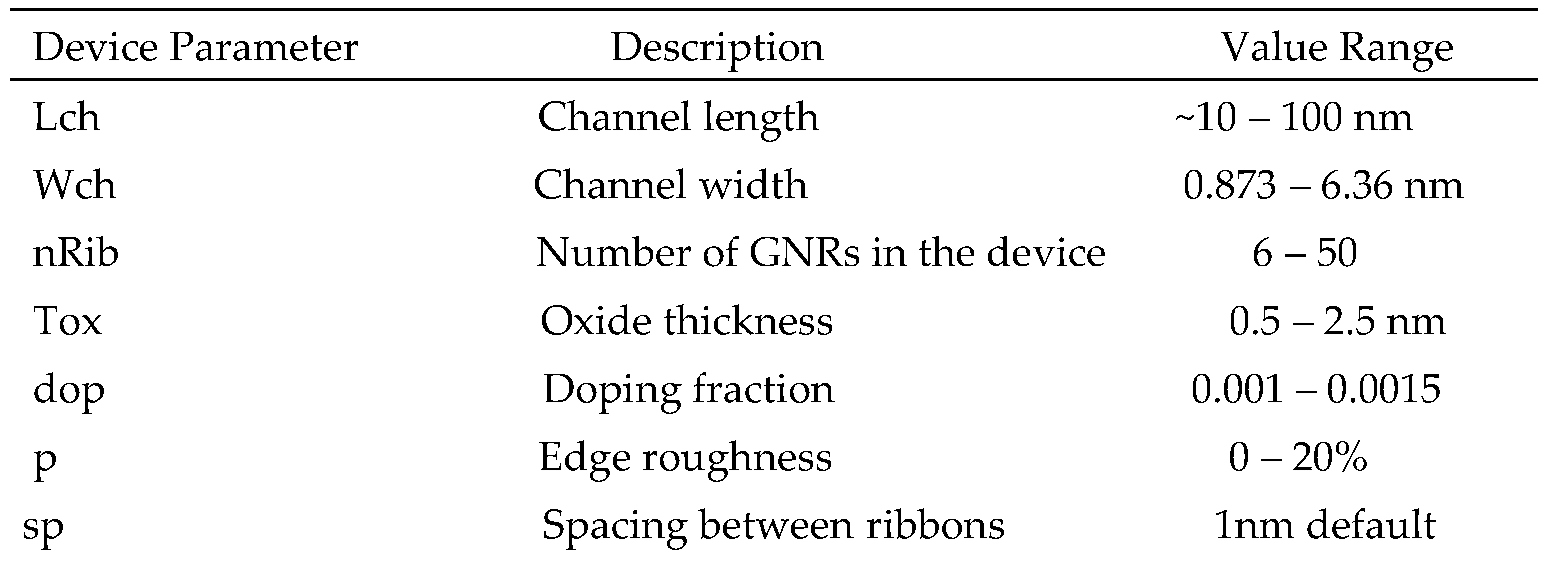
Table 1 summarizes the HSPICE model of n-/p-type GNRFET.
For the transistor level characteristics, MOS-GNRFET works well with a nominal V
DD = 0.5 V.
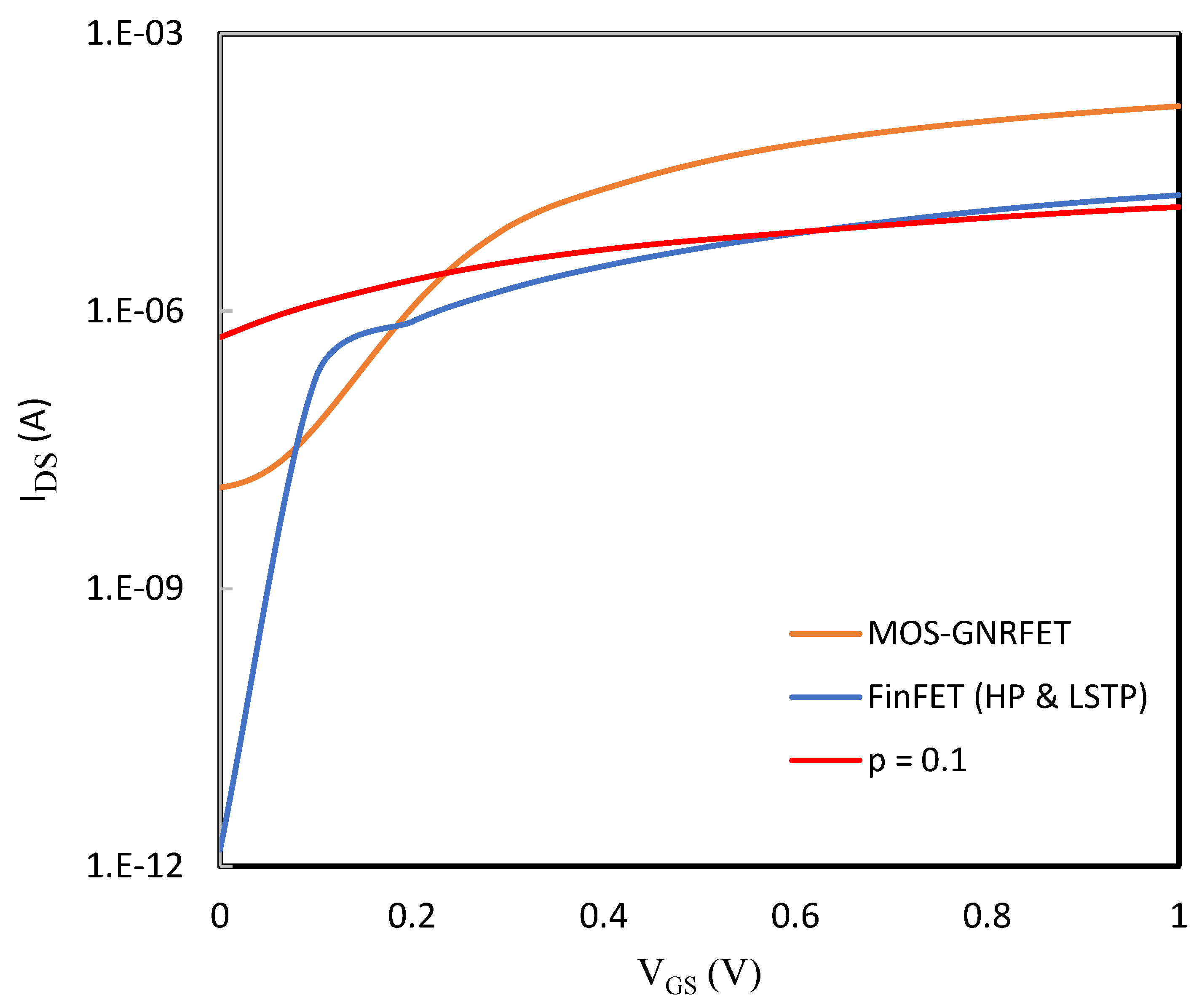
Figure 1 shows the curve of MOS-GNRFET and 10nm HP and LSTP Si-CMOS n-type transistors from PTM. For fairer comparison, we scaled the GNRFET model to match the PTM libraries. The minimum recommended nominal V
DD = 0.75 V is chosen for PTM devices.
From the plot, the ideal MOS-GNRFET has the highest I
on while PTM nano-MOSFET Si-CMOS models have better I
off, and their current ratios are given in
Table 2. As the edge roughness probability is increased to 10%, the I-V curve becomes worse in both I
on and I
off, which indicates a degradation in the performance of the device.
Here, we analyze the properties of an inverter designed with MOS-GNRFETs under V
DD = 0.5 V. Graphene nanoribbon FET is sensitive to the major sources of variation e.g., process, voltage, and temperature (PVT) that affect its performance. It is, however, important to check our design for different corners. During fabrication of transistor device, the process variation such as oxide thickness, doping concentration can vary slightly from the target specification, thereby translates to faster or slower devices. Similarly, variation in supply voltage has effect on the current drivability, and temperature can also alter the resistance of the device.
Figure 2 shows the impact of channel length, oxide thickness and line of edge roughness. Although delay increases slightly with Lch, Tox has more significant impact on the speed of MOS-GNRFET. Similarly, a higher thick oxide reduces the gate leakage, and the total power is equally reduced.
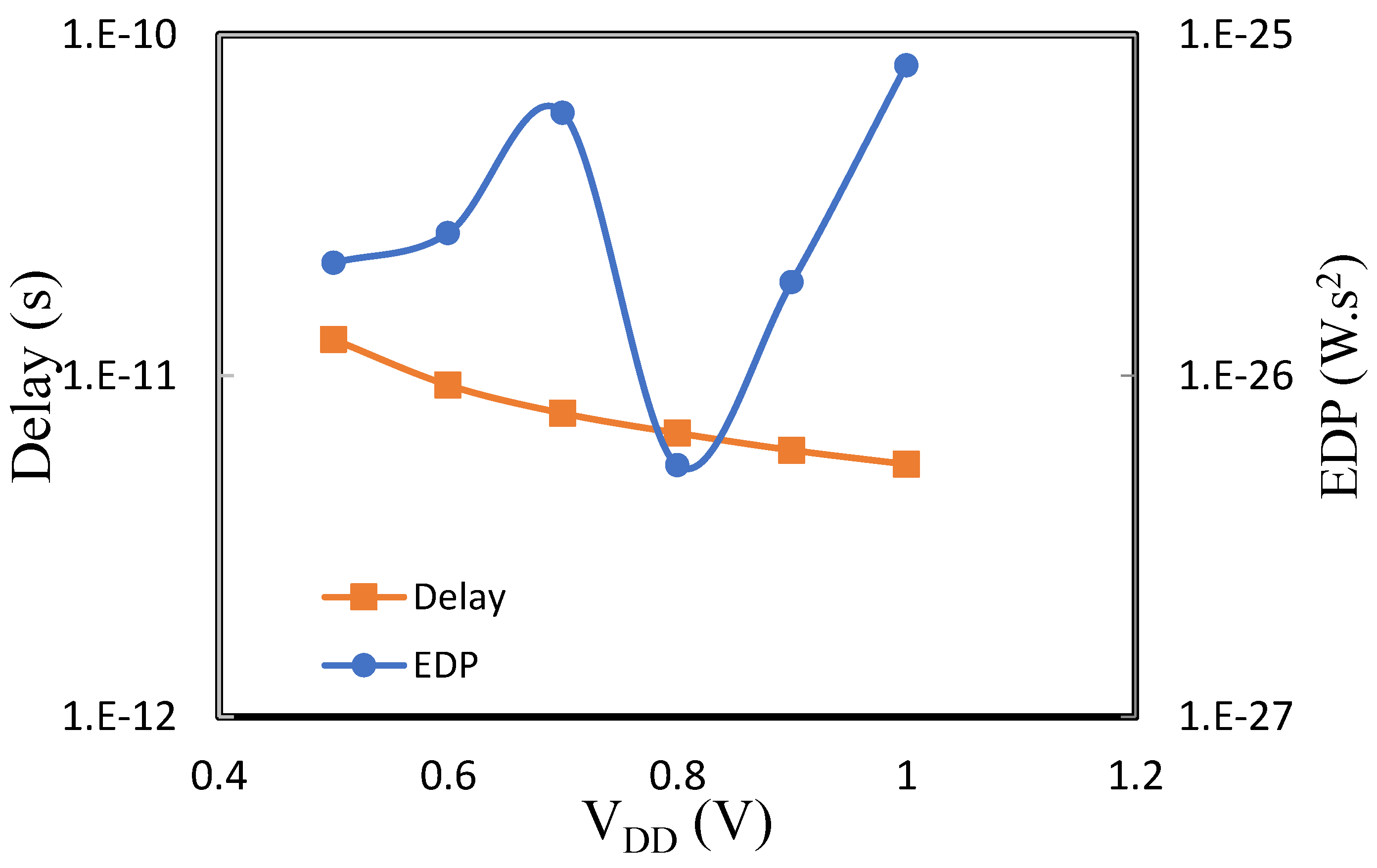
The delay in
Figure 3 decreases with V
DD because the drive current increases which largely affects the rate at which the CMOS capacitive load are charged or discharged. Unlike delay, the EDP is non-monotonic which is in consistent with the model behavior [
7]. Even though the current conduction in MOS-GNRFET model is both thermionic and BTBT (band-to-band-tunneling), its transistor properties are weakly dependent on temperature just as similar to tunnel field effect transistor.
3. Single Event Upset in SRAM Cell
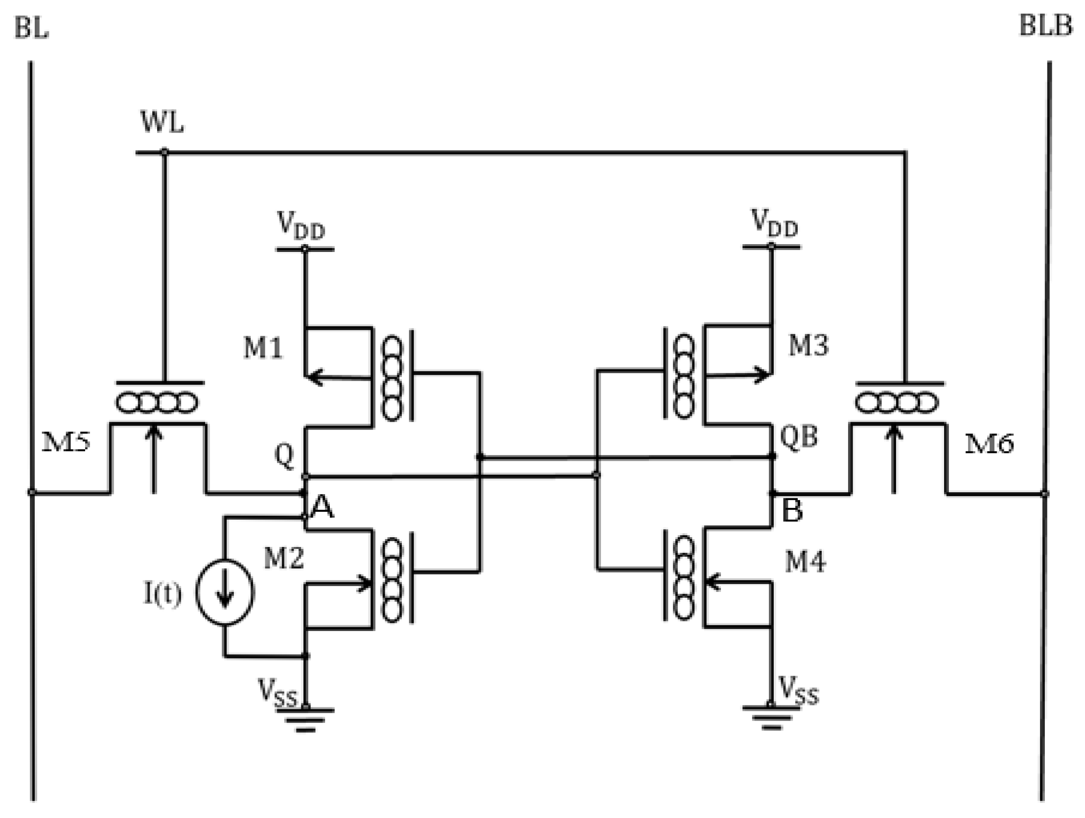
In this work, we employed the conventional 6T SRAM cell topology in
Figure 4 which comprises of the storage or memory transistors (M1-M4) and access transistors ATs (M5-M6) constructed with n- and p-type MOS-GNRFET. Transistors M5 and M6 are sized optimally to improve read and write ability and access time.
We adopted the strong drive transistors, medium access, and weak pull-up transistors whereby CR (drive to access transistor ratio) is set equal to PR (pull-up to access transistor ratio). WL denotes the control input signal applied to the gates of ATs while BL and BLB function as input or output lines depending on the mode of SRAM. Equation 3 represents the single event upset modelled with double exponential transient time current injected at sensitive nodes A and B, and the total charge collected is given as:
where the magnitude of pulse current,
= 5mA,
= 20ps and
= 40ps are time constants,
and
are collected charge and collection time, respectively.
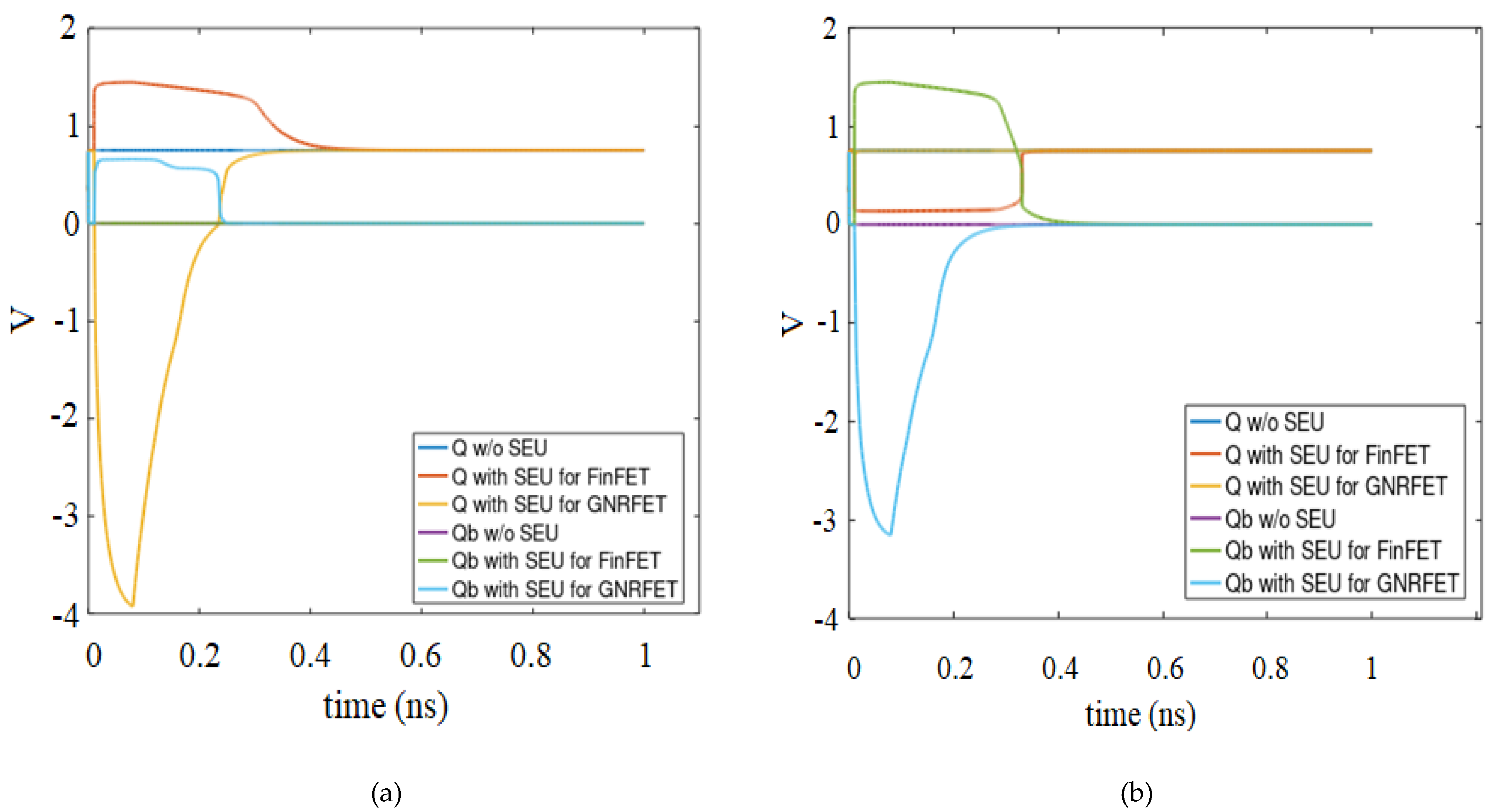
In
Figure 5(a), the output Q of an ideal GNRFET recovers faster than FinFET after radiation strike and both align with Q without SEU after 0.46 ns and 0.51 ns, respectively. Unlike Qb degradation in GNRFET, FinFET Qb is unaffected and the degradation in Q for GNRFET is also ~2.7X which infers it is more sensitive to single event transient at node A.
On the contrary, both Q and Qb of FinFET SRAM in
Figure 6 are largely affected by radiation effect at node B. The two outputs flip immediately the
due to a charge particle strike exceeds
, but it is not enough to make the node to lose its recovering potential. There is, however, 2.16X degradation observed in Qb of GNRFET SRAM. It is expected since technologies that operate with low voltage tend to be less resistant to radiation and have high soft error rate.
Stability of Graphene Nano-Ribbon FET SRAM Cell
Because of aggressive V
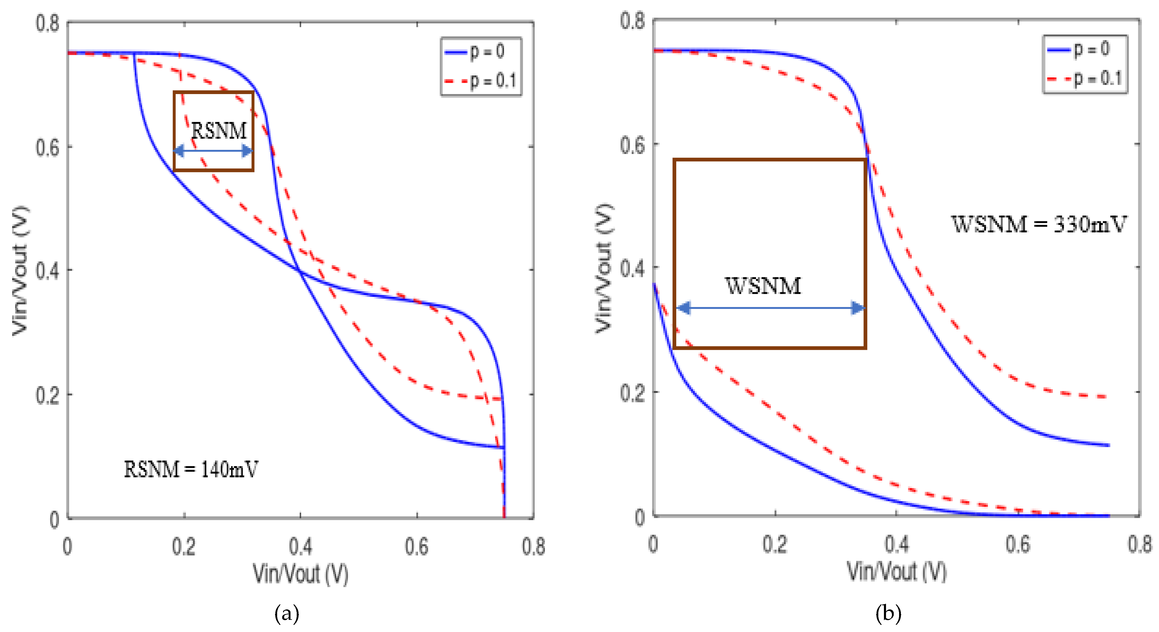
DD scaling and increased intra-die variability, the two critical metrics read and write stability of SRAM cell are major concerns. The stability also known as static noise margin (SNM) is the minimum voltage noise that can change the state of SRAM at storage node. Although there are other methods of SNM measurements, butterfly plot is considered as one of the best ways to measure the stability. It is a voltage transfer curves of the storage cell or two inverter circuitry superimposed on each other. We employed the test benches in ref. [
8] for measurements and the results are presented in
Figure 6. The read and write SNM are higher than when 10% edge roughness is introduced i.e., the robustness of SRAM is reduced with LER.
We equally investigated how SNM varies with transistor channel length or technology node and supply voltage VDD. An increase of Lch from 10nm to 25nm results in 22.1% and 19.7% increase in read and write stability, respectively. Similarly, the change in VDD from 0.5 V to 0.75 V improves the read SNM by 45 mV and write SNM by 120 mV.
5. Conclusion
In this work, transistor level properties of MOS-GNRFET and PTM nano-MOSFET models are analyzed, the impact of level of edge roughness on the performance of GNRFET is also examined. Delay, power and EDP are evaluated for different values of Lch, Tox and probability of edge roughness pr. Subsequently, the response of the single effect upset on both 6T MOS-GNRFET and FinFET SRAMs is investigated. By using circuit simulation, a transient current is injected at the drains of M2 and M4, successively, and the outputs of SRAM flip due to primary and secondary interactions caused by charged particles. However, both Q and Qb recover from the strike and the recovery time for GNRFET was estimated and compared with FinFET. More so, it is shown that the SNM of inverter can be improved by increasing the transistor channel length and/or VDD. The static noise margin of SRAM during the read operation is lower than the write SNM which concludes that SRAM is more vulnerable to flip state or data at the read mode.
Funding
The work is supported by the Louisiana State University (LSU) Economic Development Assistantships (002128), and the Office of Research & Economic Development (ORED) Grant (004475).
Conflicts of Interest
The author declares no conflict of interest.
References
- Pown, M.; Lakshmi, B. Investigation of Radiation Hardened TFET SRAM Cell for Mitigation of Single Event Upset. IEEE J. Electron Devices Soc. 2020, 8, 1397–1403. [Google Scholar] [CrossRef]
- Li, P.; Zhang, M.; Zhao, Z.; Deng, Q. Design of Analysis Platform Used for Studying Soft Error Characteristic of 3D SRAM. 2015 International Conference on Automation, Mechanical Control and Computational Engineering. LOCATION OF CONFERENCE, ChinaDATE OF CONFERENCE.
- Mahyuddin, N.M.; Russell, G. Single-Event-Upset Sensitivity Analysis on Low-Swing Drivers. Sci. World J. 2014, 2014, 1–7. [Google Scholar] [CrossRef]
- Xiang, Q.; Liu, H.; Zhou, Y. A Single-Event-Hardened Scheme of Phase-Locked Loop Microsystems for Aerospace Applications. Micromachines 2022, 13, 2102. [Google Scholar] [CrossRef] [PubMed]
- Adesina, N.O.; Srivastava, A.; Khan, A.U.; Xu, J. Phase Noise and Jitter Measurements in SEU-Hardened CMOS Phase Locked Loop Design. 2021 IEEE International IOT, Electronics and Mechatronics Conference (IEMTRONICS). LOCATION OF CONFERENCE, CanadaDATE OF CONFERENCE; pp. 1–6.
- Choudhury, M.R.; Yoon, Y.; Guo, J.; Mohanram, K. Graphene Nanoribbon FETs: Technology Exploration for Performance and Reliability. IEEE Trans. Nanotechnol. 2010, 10, 727–736. [Google Scholar] [CrossRef]
- Chen, Y.-Y.; Sangai, A.; Gholipour, M.; Chen, D. Graphene nano-ribbon field-effect transistors as future low-power devices. 2013 IEEE International Symposium on Low Power Electronics and Design (ISLPED). LOCATION OF CONFERENCE, ChinaDATE OF CONFERENCE; pp. 151–156.
- Saxena, V. SRAM Static Characterization. Technical report, Boise State University. Retrieved from https://www.eecis.udel.edu/~vsaxena/courses/ece518/Handouts/SRAM%20Characterization.pdf.
|
Disclaimer/Publisher’s Note: The statements, opinions and data contained in all publications are solely those of the individual author(s) and contributor(s) and not of MDPI and/or the editor(s). MDPI and/or the editor(s) disclaim responsibility for any injury to people or property resulting from any ideas, methods, instructions or products referred to in the content. |
© 2023 by the authors. Licensee MDPI, Basel, Switzerland. This article is an open access article distributed under the terms and conditions of the Creative Commons Attribution (CC BY) license (https://creativecommons.org/licenses/by/4.0/).
