1. Introduction
The importance of research on perovskite solar cells is strongly influenced by the notable improvement in their energy conversion efficiency (PCE), given that reports indicate that in just over 10 years they have had an increase in their PCE of 3.8% to 25.7%[1—4], however, the Shockley-Queisser limit for single-junction perovskite solar cells is ≈33%, it also presents an extension to multijunction, depends on the junction it could be from 44% to 65%[
5,
6]; the typical structure of a perovskite solar cell consists of an electron transport layer (ET L), a perovskite layer, which is the active material, and a hole transport layer (HTL); each of the layers are very important, but in concrete, the loss of efficiency is highly related to the ability of the ETL to transport the photogenerated electrons.
Within the structure of solar cells, the electron transport layer plays a vital role, since depending on its morphology, the type of material from which it is built and its physical properties, it will be used to provide better stability, increase the lifetime, and offer higher PCE, some of the most widely used materials are metal oxides, such as TiO
2[
7,
8,
9], ZnO[
10,
11,
38], SnO
2[
13,
14,
15], SiO
2[
16], ZrO2[
17,
18], each material provides specific advantages[
19].
Recent studies indicate that nanostructured TiO2 offers greater stability, a longer useful life, and a higher percentage of energy conversion. An electron transport layer must comply with some requirements: 1)well-matched energy alignment to trigger electron transfer while blocking holes; 2) high transparency to allow efficient light harvesting; 3) excellent electron mobility to minimize charge accumulation; and 4) easy access to starting materials with high chemical resistance to perovskite solvents[20–23], and TiO2 offers high performance as an ETL in PSC’S due to their fitting of the TiO2 conduction band alignment with the perovskite layer[
24,
25].
The TiO
2 is an n-type semiconductor[
26], is chemically very stable, absorbs electro- smagnetic radiation near the UV region, and its band gap is around 3 eV[
27]. Titanium oxide has four crystalline phases anatase, rutile, brookite, and a high pressure type ff-PbO
2, The rutile phase is the only one to be thermodynamically stable[
28], while the other two, anatase and brookite, are metastable and transform into rutile when heated[
29].
The implementation of TiO
2 nanocolumns as ETL presents great advantages com- pared to flat and mesoporous layers when structuring a PSC[
30], since it provides greater stability and efficiency, by way of some adventages: i) enhance the contact zone between perovskite and ETL, and increase exciton generation, ii) the 1D morphology offered a directive path for electron transport to the TCO substrate and minimize resistance to charge transport, iii) Larger nanorods improve the light scattering and absorption properties of the PSCs[
32]. It has been found that the presence of semiconductor metal oxides optimize the ETL/perovskite interface, as well as enhances perovskite layer growth[
33]. The ETL geome- try plays an important role in the PSC’s to maximize device performance [
34], furthermore, the range transparency of TiO
2 is greater than 85%[
35]. The study of the implementation of TiO
2 nanocolumns is not biased towards its properties as a photocatalyst, and the importance of continuing to study it lies, especially with this structured morphology that can provide improvements to current technology. There exist a variety of methods to deposit compact and nanostructured TiO
2 from chemical (CVD) and physical (PVD) techniques; however, the deposition of transparent oxide thin films by sputtering offers excellent quality properties in these materials, near the low coast. There is a huge research gap around the preparation of nanomaterials through the sputtering technique, in fact, there are very few reports of thin film growth using GLAD in sputtering, this work offers an accurate report of nanocolumnal growth of TiO
2 in the anatase phase using DC sputtering, where such nanocolumns offer the essential characteristics that a high-quality ETL requires.
2. Materials and Methods
2.1. Preparation ofTiO2 bi layer films
For the growth of the TiO
2 bilayer films, developed by the reactive DC magnetron sputtering technique, a pure 2" diameter titanium target was used, in a reactive atmosphere of Argon and Oxygen with the following proportions: 5/40, 10/40, 15/40 sccm respectively of O
2/Ar, the power used for the different deposits was 120 W and 140 W, on two different substrates, namely glass and silicon (100), the deposits were made at a vacuum pressure of the order of 10
−3 Torr, for 60 min, with a presputtering of between 5-20 min, depending of the time it took's for the plasma to reach stability, the deposition temperature was maintained around 22°C; the deposit of the first layer was carried out in a normal configuration under the mentioned specifications, while the growth of the second layer was carried out in a configuration of GLAD at an angle of inclination of 70°, during 90 min, maintaining the vacuum pressure at ~10
−3 Torr, and the concentration of gases in the atmosphere (O
2 /Ar) was 5/40 and 10/40 sccm, and the power of deposition was 120W and 140W, they kept the same power for both the first and second thin film. In
Table 1, all of this can be observed.
2.2. Characterization
For the characterization of the samples obtained, the following techniques were used: X-ray diffraction, this characterization was carried out in a Rigaku Dmax2100 brand equipment. The diffractometer is equipped with a vertical goniometer (185mm), a Ni filter, and a scintillation counter. The radiation generator tube is made of copper (K
α=1.5406 Å), the maximum power is 2 kW (50 kV and 40 mA); however, the measurements in the materials use 30 kV and 20 mA (600 W). The irradiation zone in the sample was controlled by the divergence grating (DS), there are dispersion slits (SS) and reception slits (RS). The step size resolution of the goniometer is 0.005° [
36]. A second analysis was performed with a PerkinElmer Spectrum GX Fourier Transform Infrared (FTIR) Spectrophotometer with AutoIMAGE Coupled Microscope. The FTIR operates in the Mid and Near Infrared (MIR and NIR) and has four accessories. The one used to measure the samples was the Total Attenuated Reflectance (ATR) with Diamond tip and Zinc Selenide (ZnSe). The ATR with ZnSe has a controlled heating system from room temperature to 120 °C [
30]. Another optical characterization from which we measure the transmission of light corresponds to the transmission percentage (%T) that was obtained from a PerkinElmer UV-Vis ellipsometer, precisely model Lambda 35, which operates at wavelengths from 200 to 1100 nm. The last characterization was carried out to know the morphological characteristics; the morphology was analyzed by field emission scanning electron microscopy (FE-SEM-TESCAN MIRA 3 model).
3. Results
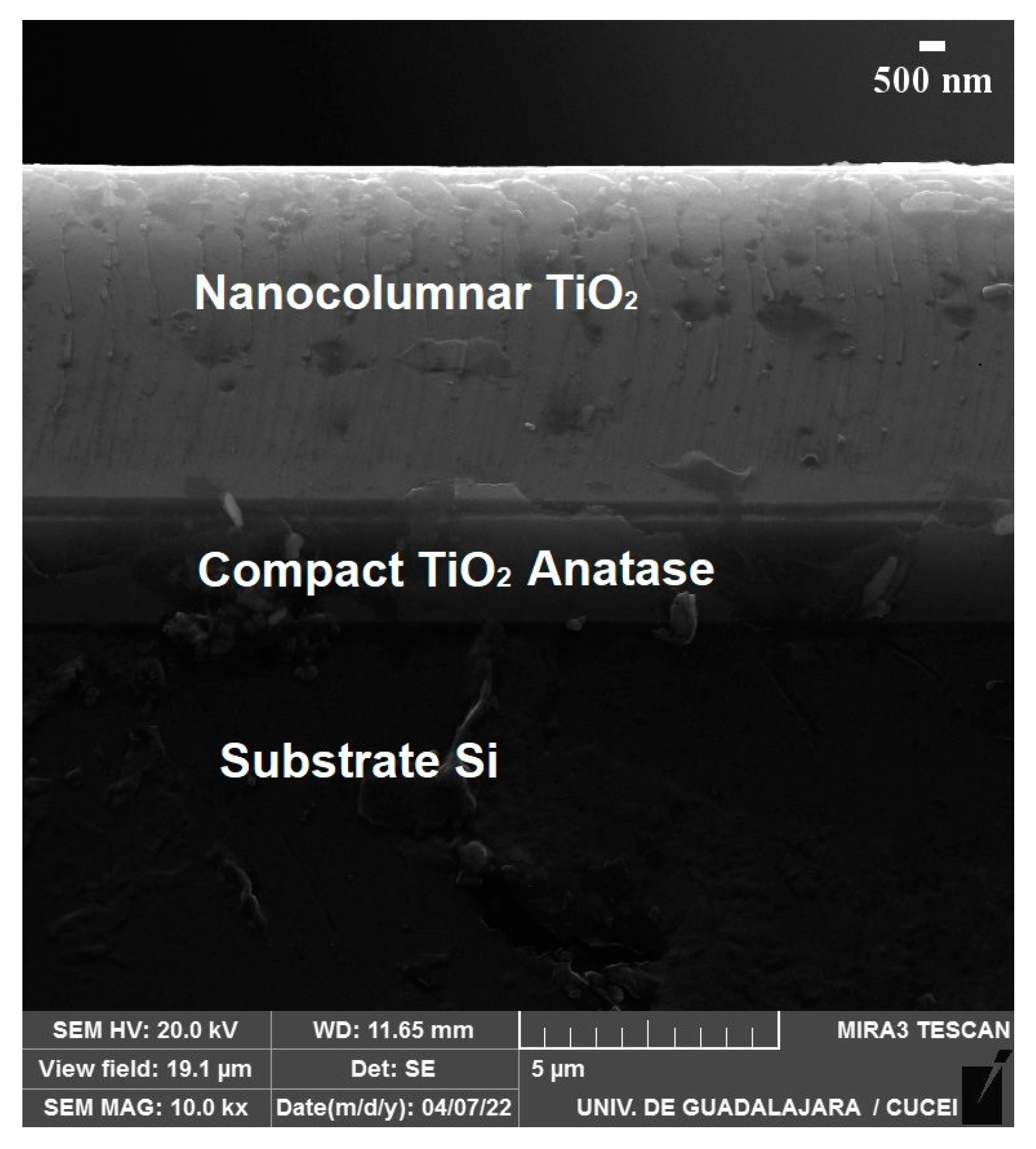
Figure 1 shows the profile for the complete structure of one of the grown bilayer samples. In this image it is possible to observe three regions, the lower part corresponds to the substrate, which in this case is Si (100), and the intermediate region corresponds to the compact crystalline TiO
2 layer that was deposited under normal sputtering conditions. Finally, the upper region corresponds to the columnar TiO
2 layer that was grown under sputtering conditions of the glazing angle. In general, the compact layer has a thickness (∼ 2
μ m) while the columnar layer has an average thickness of several micrometers and presents a strong dependence with the deposition conditions such as the composition of the sputtering atmosphere and the sputtering power used, in addition to the fact that the surface on which the bilayer samples were structured is different depending on the deposition conditions of the first layer.
3.1. Compact TiO2 layer
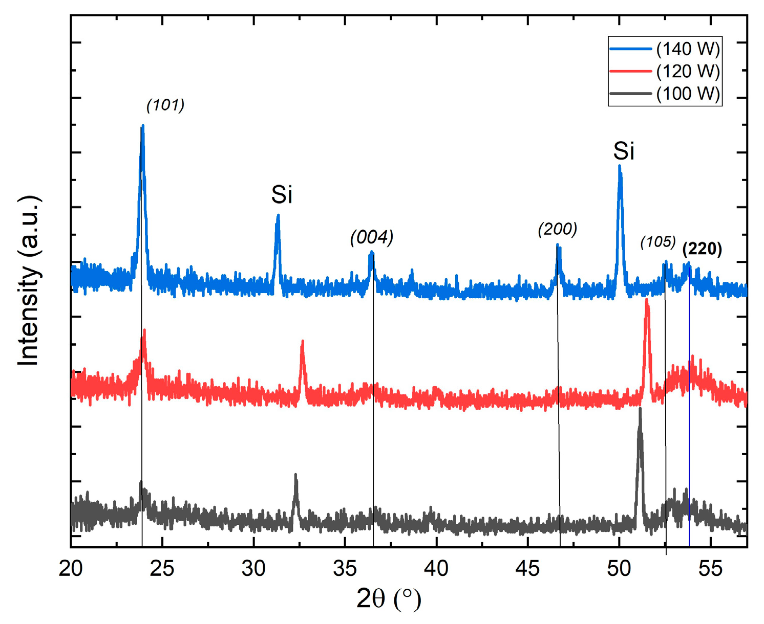
The diffractograms in
Figure 2 shows a typical TiO
2 X-ray diffraction pattern corre- sponding to the anatase
1 crystalline phase. The three thin layers were deposited under the same sputtering atmosphere conditions (10
O2/40
Ar) in normal sputtering condition, varying only the deposit power to 100W, 120Wand 140W, a diffraction peak is identified at an angle 2
θ = 25.4 as principal maximum, this peak corresponds to the signal of the plane (101) of the structure tetragonal anatase typical of TiO
2. Film deposited at 140 W shows better definition of the crystallographic planes, and in it, in addition to this maximum, it is possible to identify the peaks associated with the (004), (200) and (105) planes at 2
θ equal to 37.8°, 48.08° and 53.89° respectively. Regarding the effect of the deposit power in the structure 2 X-ray diffraction analysis performed on samples can be observed from the diffraction patterns that with the increase in power results in a better crystalline quality, this is reflected in obtaining sharper and higher diffraction peaks.
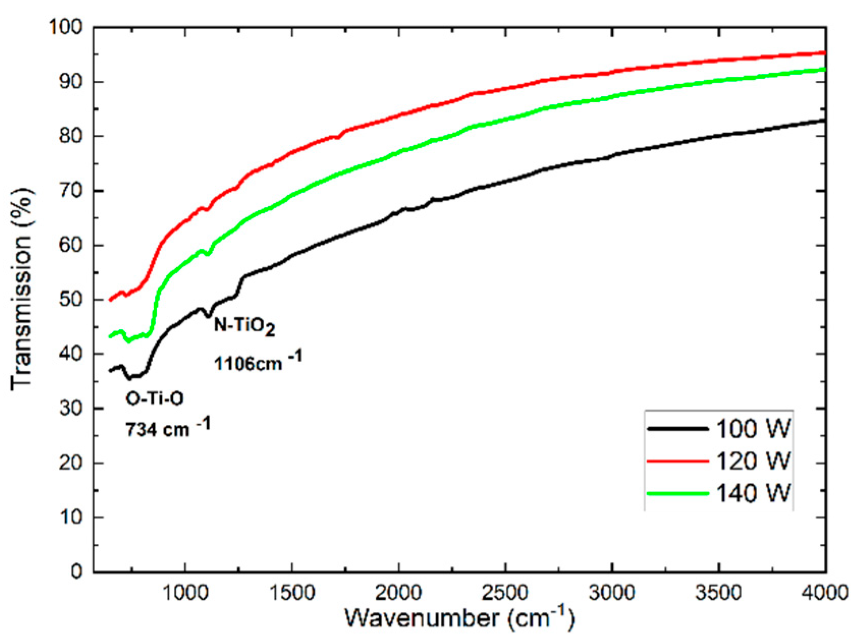
The results of ATR spectroscopy are shown in figure 3. In this characterization, two absorp- tion bands can be identified that correspond to Ti-O-Ti bond when there is an incidence of light with a wave number of 734
cm−1 and a bond of N− TiO
2 for a wavenumber of 1106
cm−1[
31].
3.2. Nanocolumnar TiO2 layer
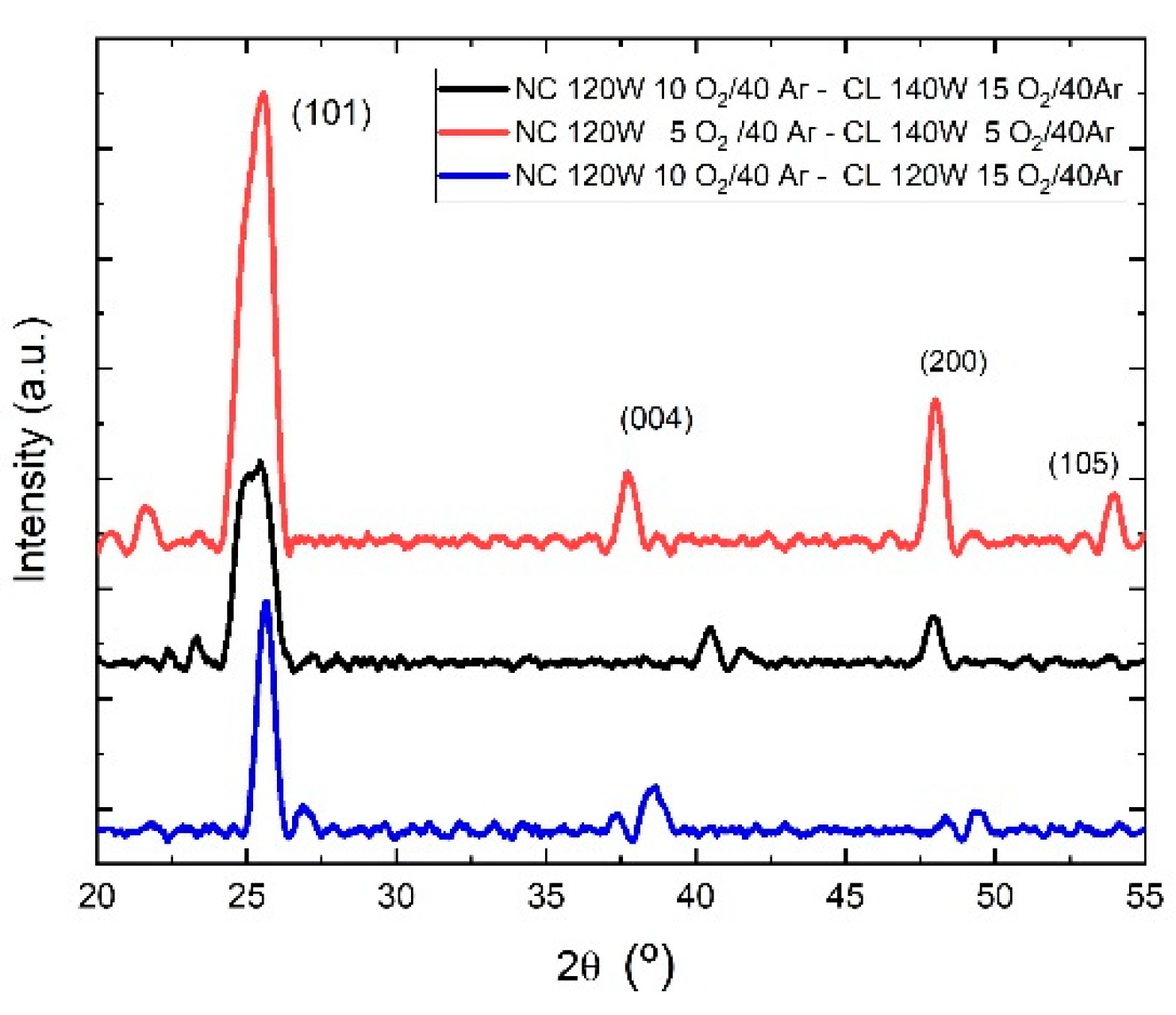
The diffractogram obtained from the XRD characterization for the samples whose film was thermally treated at 500°C and 400°C are shown in
Figure 4, these films present a crystalline structure that we identify as anatase, a phase identified by the crystallographic planes (101), (004), (200). More specifically, sample M4 presents crystallographic planes (101), (004), (200), and (105) at 2
θ = 25.35°, 37.9°, 48.0° ,53.9°. respectively; likewise, M3 clearly presents the (101) and (200) planes at 2
θ = 25.58°, 25,21°, 47.96°, 47.99°, respectively. Sample M6 presents a single intensity peak at 2
θ = 25.61 which corresponds to the crystallographic plane (101).
The XRD measurements made it possible to determine the crystallite size (D) and the lattice parameters. The value of (D) was calculated from the Scherrer equation, while the lattice parameters were calculated using Bragg’s law. To calculate the crystalline parameters a and b, the interplanar distance corresponding to the signal identified by the crystallographic plane (200) was used, while the parameter c was calculated from the peak (101), the said signal being the one with the highest intensity and the most important. To identify the anatase phase of TiO2.
The vibrational properties of the deposited TiO
2 films were analyzed by Fourier transform infrared (FTIR) spectroscopy. The results obtained are shown in
Figure 5.
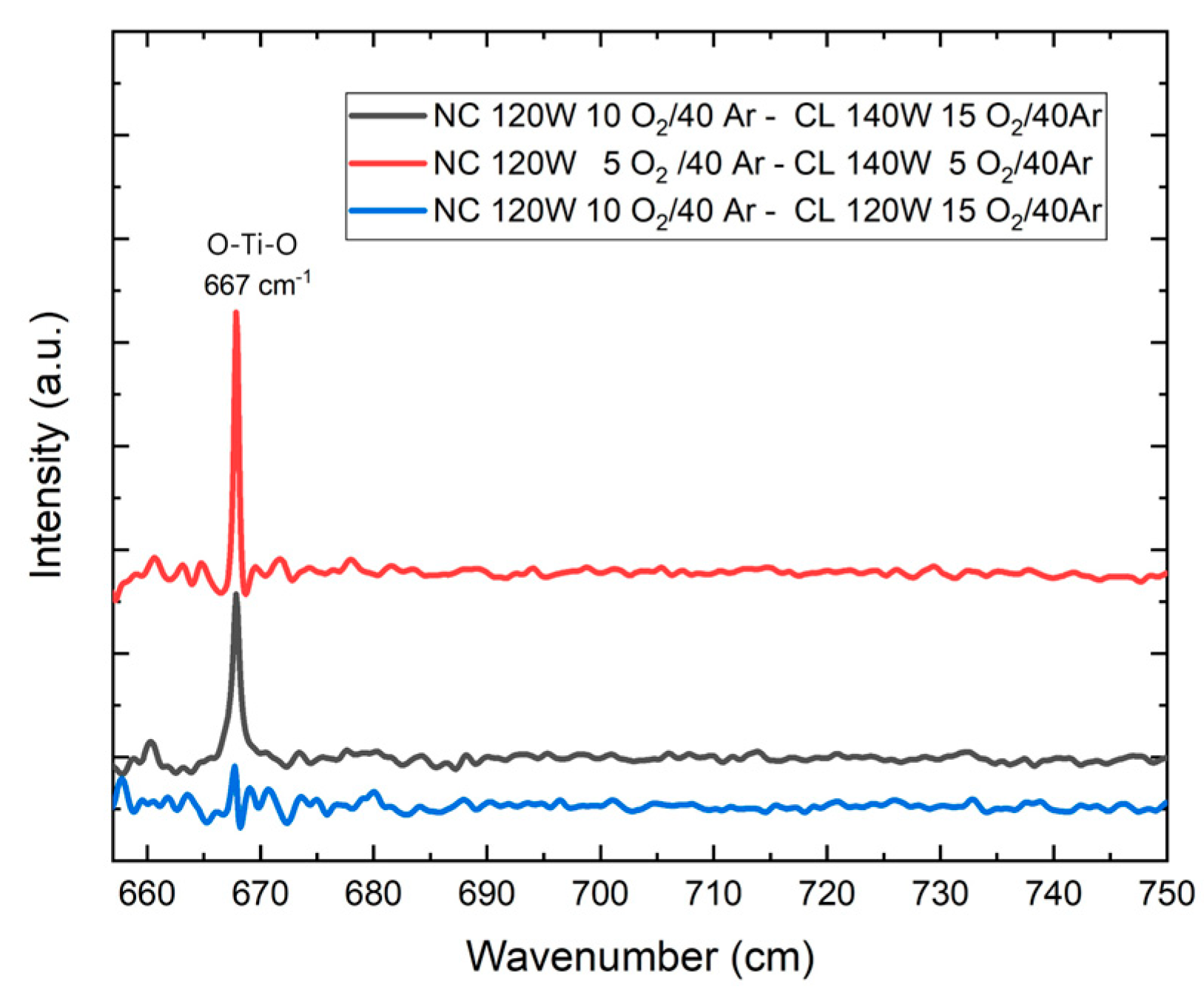
Figure 5 shows the appearance of an absorption band at a wave number of 667 cm
−1, which corresponds to the O-Ti-O bond of TiO
2 [
37].
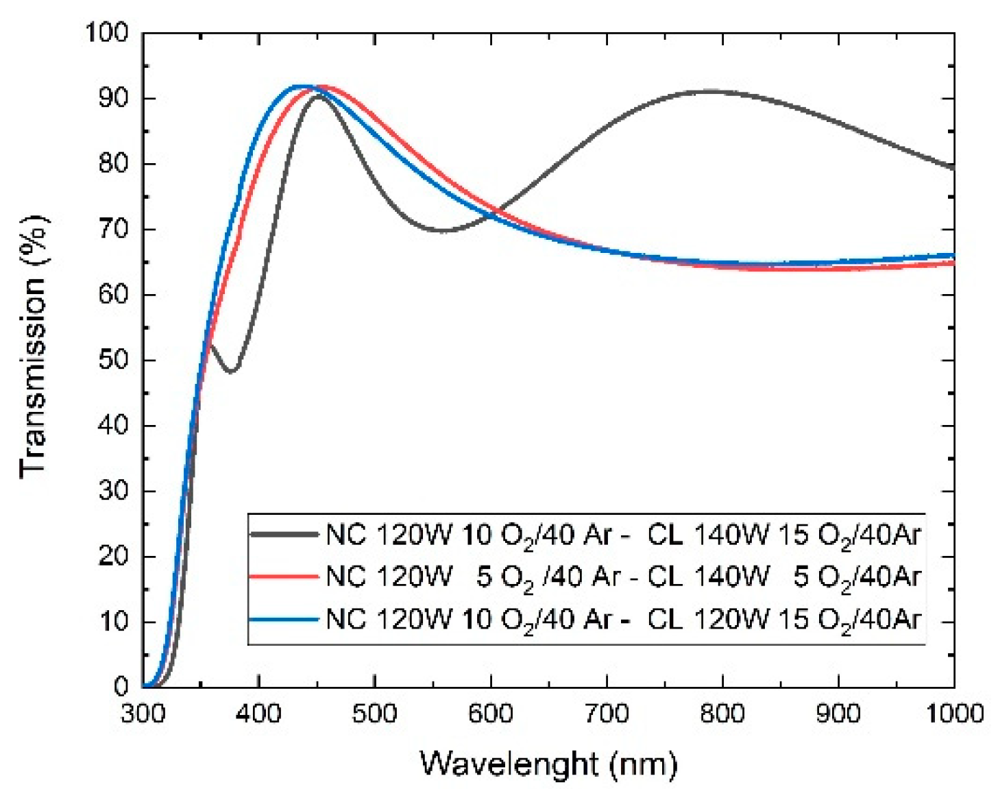
Figure 6 shows the UV-vis spectrum of TiO
2 bilayer films. From the transmission spectra it can be seen that most of the samples present a maximum of light transmission in a range of
λ of 350 − 600 nm, the maximum transmission percentage oscillates between 90% and 95%.
Figure 7 was made using the Tauc’s method, it is possible to determine the optical band gap. The growth of Tauc’s curve becomes linear when the photon energy coincides with the value of the band gap.
To observe the nanocolumns structure of the TiO2 films, a morphological characterization was carried out using the scanning electron microscopy technique, both on the surface and on the profile of some of the deposited samples.
In
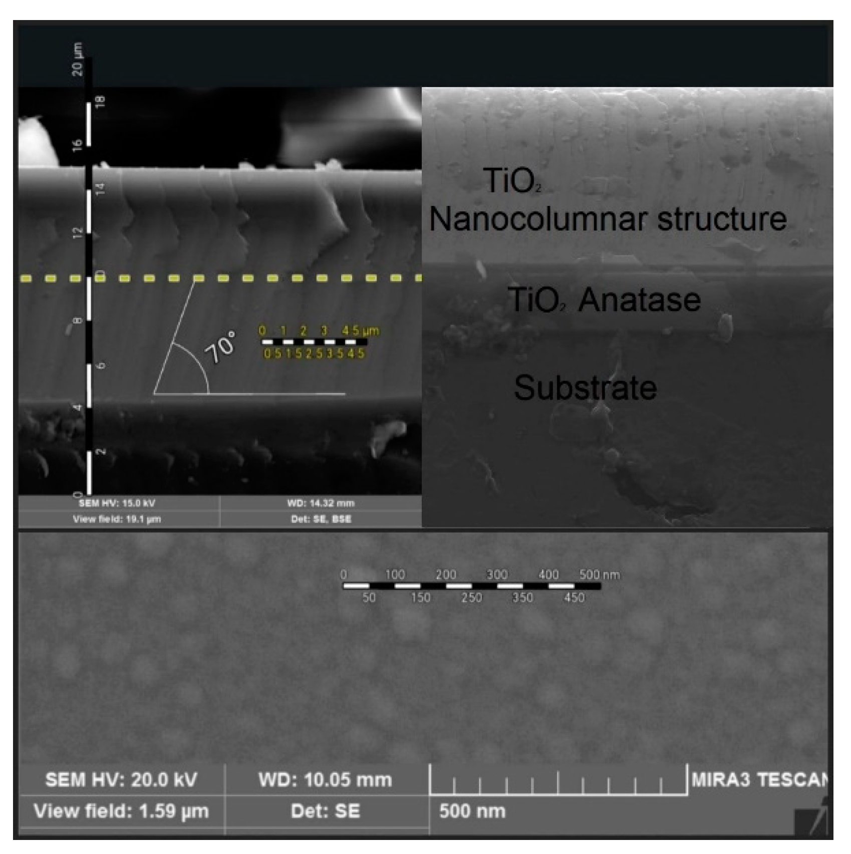
Figure 8, there are presented three different micrographs of the same sample with the best morphology of all our samples; in the upper right micrograph an SEM image of the profile is observed (cross section) where the three regions of the sample are identified: substrate, TiO
2film crystalline with anatase phase and TiO
2film with nanocolumnal growth also with an anatase crystalline phase. The upper left image corresponds to the same profile image, but with contrast enhancement to better identify the aforementioned areas; additionally, a graduated ruler is added to the image to facilitate the approximation of the thicknesses and the angle of inclination of the nanocolumns. The lower micrograph shows a SEM image of the sample surface in which a distribution of uniform islands formed from the nanocolumnar growth of the second layer is observed.
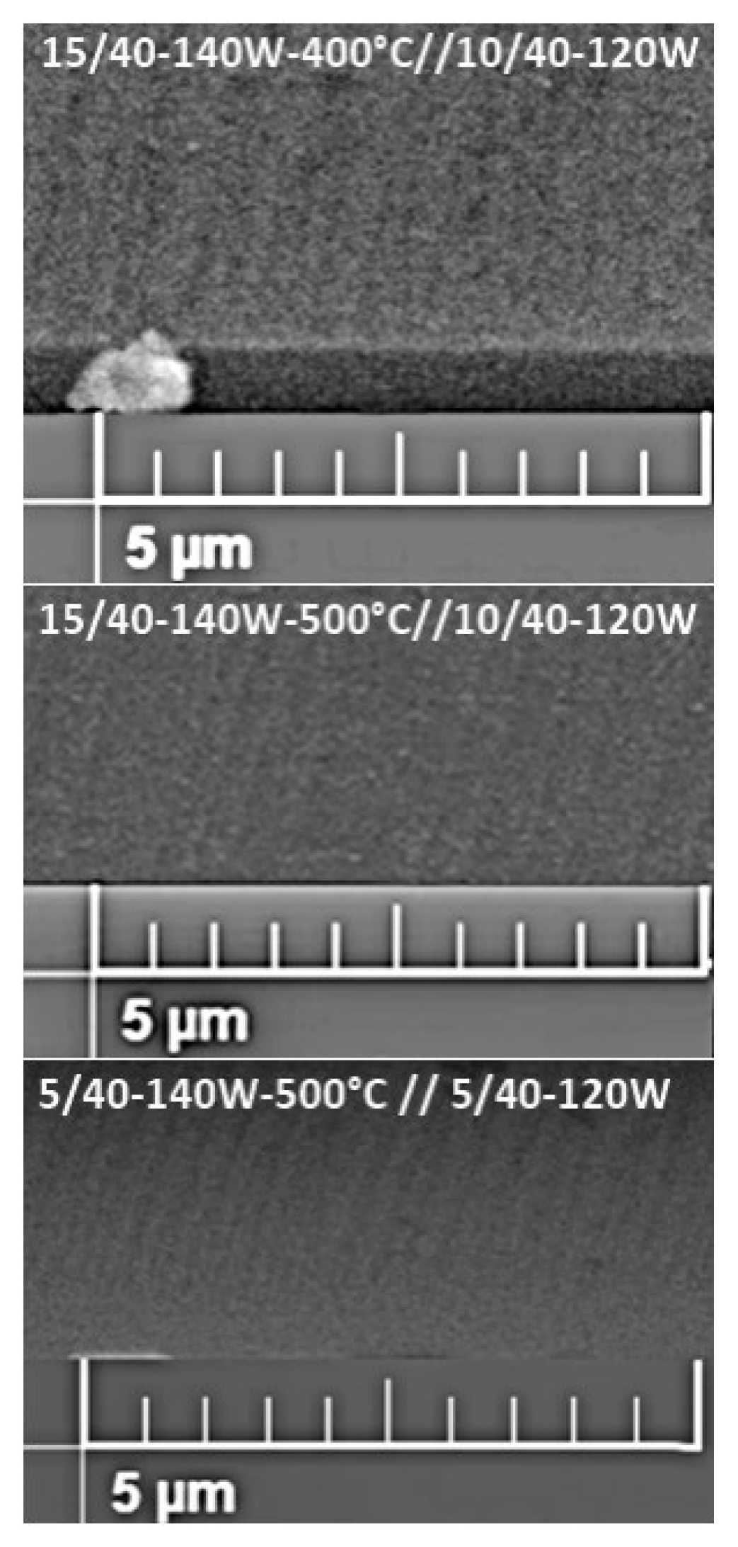
Figure 9 shows the SEM profile of the TiO
2 nanocolumnal layer. In the three samples, there is possible to observe a well-defined filaments which correspond to the height of the nanocolumns. It can be observed that there is a relationship between the deposition angle of the nanocolumns and the inclination they exhibit. Considering a deposition angle of 70 degrees, nanocolumns inclined at values close to this angle are being observed. The measured angles in the inclination of the nanocolumns range from 68 to 80 degrees. This image is of great value as it provides evidence of the existence of the columns, which are closely related to the crystalline quality of the substrate.
Figure 10 correspond to the surface SEM imagenes of the bilayer TiO
2 films. The three micrographics shows small circles with an approximate diameter of 70 nanometers. This image, together with the SEM profile image 8, allows us to confirm the existence of nanocolumns grown using the magnetron sputtering technique with the oblique angle technique.
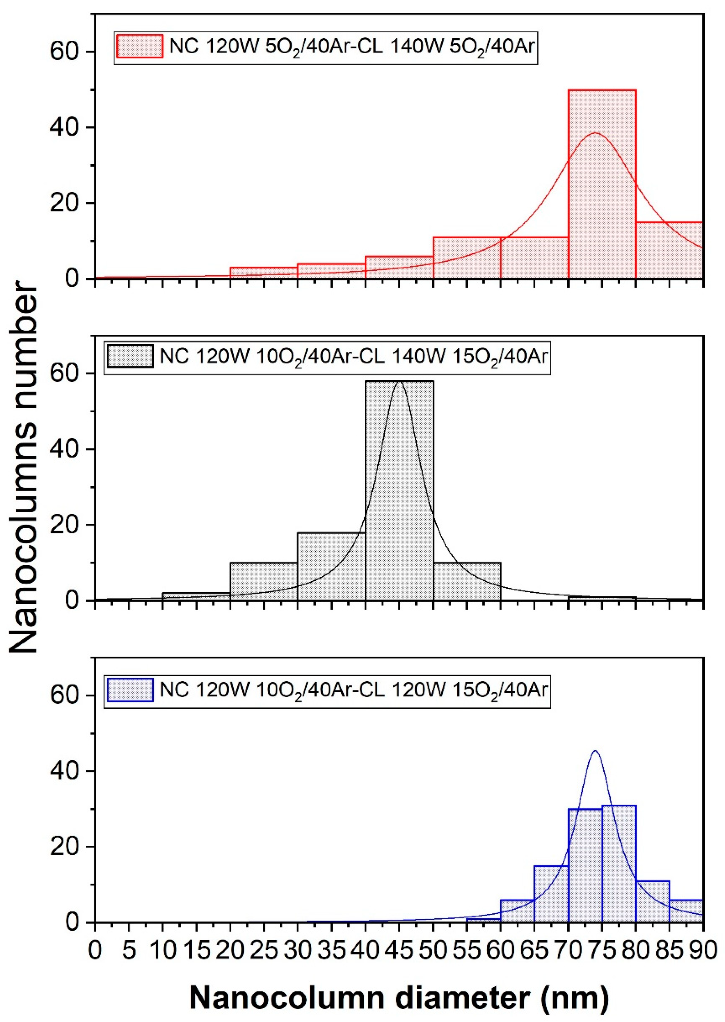
The histogram to compare the diameters of the nanocolumns, for each of the samples, are showed in
Figure 11. It can be observed that the average diameter in each of the bi-layer films shows a significant variation. This variation can be explained in the discussion of the study, where factors such as film composition, deposition parameters, thermal treatment, among others, will be considered. These factors can influence the formation and growth of the nanocolumns, which in turn affects their average size.
4. Discussion
In this research, it was found that the sample with the best crystalline quality is sample M4. Was associated the high crystallinity with the low presence of oxygen during the growth of the compact layer. Within the scientific literature, it is becoming increasingly clear that epitaxial growth in multilayer films[
38] is favored by the crystalline quality of the first layer. In addition to the above, in the deposition using the oblique angle technique was chosen to grow the nanocolumns under the same atmospheric conditions, which also proved to be suitable, especially in terms of crystalline quality. Evidence of this is seen in the XRD patterns and IR analysis, where the absorption band corresponding to the O-Ti-O bond is better defined for this sample, and the XRD peak associated with the (101) direction presents a higher intensity compared whit the other two samples.
As for samples M3 and M6, their nanocolumnar layer was deposited under identical parameters. However, there were a couple of differences in the compact layer that influenced the results. Both were grown under the same atmospheric conditions but with a variation in the deposition power (140W and 120W, respectively). Additionally, they underwent thermal treatment at 500 °C and 400 °C, respectively. In this case, we believe that the 400°C thermal treatment improved the crystalline quality of sample M6, resulting in a nanocolumnar layer with better crystallinity compared to M3. Regarding the intensity of the band associated with TiO2, M3 exhibits higher intensity.
All three layers are highly transparent, allowing light to pass through up to 90%. However, in this case, samples M4 and M6 are more transparent in the range of 350 to 600 nm, while M3 is more transparent in the range of 600 to 1000 nm, and presents a band gap with values between 3.7 and 3.8 eV, therefore, it fully complies with the optical condition to be used as ETL.
The morphology of the films is evident through superficial and profile SEM analyses. In the profile SEM image, sample M4 shows a better definition of the filaments, and in general, a strong relationship was found between the deposition angle in the GLAD configuration and the inclination of the nanocolumns. The superficial SEM images for samples M3 and M6 exhibit homogeneity in terms of the distribution and diameter of the nanocolumns. For M3, the nanocolumns have an average diameter of 43.9 nm, while for M6, the average diameter is 73.8 nm.
The homogeneity observed can be attributed to the optimal oxygen concentration during the deposition of the nanocolumnar layer. As for sample M4, despite having better physical properties, it exhibits inhomogeneity in the distribution and size of the nanocolumns. Nevertheless, the average diameter of the nanocolumns is 66.8 nm.
5. Conclusions
It is concluded that It was possible to obtain a columnar growth in bilayer films of TiO2 deposited through the reactive DC magnetron sputtering technique in grazing angle configuration (GLAD). TheThe optimal parameters to achieve a columnar layer of TiO2 are related to high deposition powers, low oxygen concentrations, and ideal thermal treatment. In addition to the influence of the crystalline quality of the first layer of TiO2, achieving columnar growth in the deposit in the grazing configuration is of the utmost importance to obtain the desired morphology, because, from this, an epitaxial growth in the islands that give rise to the columns is anticipated or not. The best results for columnar growth in the second layer are obtained from films whose layer one was thermally annealed at 500 °C.
Author Contributions
Conceptualization, J.Ortega and J.Berumen.; methodology, P.Rosales, J.Ortega and F.Avelar.;validation, J. Araiza., H.Tototzintle. and J.Ortega.; formal analysis, P.Rosales.; investiga- tion, P.Rosales.; resources, E.Sigala.; data curation, F.Avelar.; writing—original draft preparation, P.Rosales.; writing—review and editing, J.Ortega and H.Mendez.; visualization, P.Rosales.; supervi- sion, J.Ortega.; project administration, J.Berumen, H. Tototzintle and J. Araiza.
Funding
This research work has been supported by a master’s scholarship from CONACYT.
Institutional Review Board Statement
Not applicable
Informed Consent Statement
Not applicable
Acknowledgments
We appreciate the support of CONACYT for their contribution to the devel- opment of science and technology. We also extend our gratitude to CINVESTAV Querétaro and the University of Guadalajara for allowing us to carry out some characterizations in their laboratories.
Conflicts of Interest
The authors declare no conflict of interest.
| 1. |
The diffraction planes of the samples were identified from the XRD patterns and a correspondence was found with the #21 − 1272 file reported in the JADE ®program. |
References
- Jeng, J.-Y.; Chiang, Y.-F.; Lee, M.-H.; Peng, S.-R.; Guo, T.-F.; Chen, P.; Wen, T.-C. CH3NH3PbI3Perovskite/Fullerene Planar-Heterojunction Hybrid Solar Cells. Advanced Materials 2013, 25, 3727–3732. [Google Scholar] [CrossRef] [PubMed]
- Kojima, A.; Teshima, K.; Shirai, Y.; Miyasaka, T. Organometal Halide Perovskites as Visible-Light Sensitizers for Photovoltaic Cells. Journal of the American Chemical Society 2009, 131, 6050–6051. [Google Scholar] [CrossRef] [PubMed]
- Interactive Best Research-Cell Efficiency Chart. (s. f.-b). Photovoltaic Research | NREL. https://www.nrel.gov/pv/interactive- cell-efficiency.html.
- Bati, A.S.R. ; Zhong, Y.L. ; Burn, P.L. et al. Next-generation applications for integrated perovskite solar cells. Commun Mater 4, 2 (2023). [CrossRef]
- Albrecht, S.; Rech, B. Perovskite solar cells: On top of commercial photovoltaics. Nature Energy, 2017, 2. [CrossRef]
- Sha, W. E. I.; Ren, X.; Chen, L.; Choy, W. C. H. The efficiency limit of CH3NH3PbI3 perovskite solar cells. Applied Physics Letters 2015, 106, 221104. [Google Scholar] [CrossRef]
- Arshad, Z.; Shakir, S.; Khoja, A. H.; Javed, A. H.; Anwar, M.; Rehman, A.; Javaid, R.; Qazi, U. Y.; Farrukh, S. Performance Analysis of Calcium-Doped Titania (TiO2) as an Effective Electron Transport Layer (ETL) for Perovskite Solar Cells. Energies 2022, 15, 1408. [Google Scholar] [CrossRef]
- Khorasani, A.; Marandi, M.; Iraji zad, A.; Taghavinia, N. Electron transport engineering with different types of titanium dioxide nanostructures in perovskite solar cells. Journal ofAlloys and Compounds 2023, 936, 168055. [Google Scholar] [CrossRef]
- Zhao, F.; Guo, Y.; Yang, P.; Tao, J.; Jiang, J.; Chu, J. Effect of Li-doped TiO2 layer on the photoelectric performance of carbon- based CsPbIBr2 perovskite solar cell. Journal of Alloys and Compounds 2023, 930, 167377. [Google Scholar] [CrossRef]
- Liu, G.; Zhong, Y.; Mao, H.; Yang, J.; Dai, R.; Hu, X.; Xing, Z.; Sheng, W.; Tan, L.; Chen, Y. Highly efficient and stable ZnO-based MA-free perovskite solar cells via overcoming interfacial mismatch and deprotonation reaction. Chemical Engineering Journal 2022, 431, 134235. [Google Scholar] [CrossRef]
- Pang, Z.; Yang, S.; Sun, Y.; He, L.; Wang, F.; Fan, L.; Chi, S.; Sun, X.; Yang, L.; Yang, J. Hydrophobic PbS QDs layer decorated ZnO electron transport layer to boost photovoltaic performance of perovskite solar cells. Chemical Engineering Journal 2022, 439, 135701. [Google Scholar] [CrossRef]
- Muhammad, S.; Nomaan, A. T.; Olaoye, A.; Idris, M. I.; Rashid, M. Concentration dependence of physical properties of low temperature processed ZnO quantum dots thin films on polyethylene terephthalate as potential electron transport material for perovskite solar cell. Ceramics International 2022, 48, 31559–31569. [Google Scholar] [CrossRef]
- Kim, M.; Jeong, J.; Lu, H.; Lee, T. K.; Eickemeyer, F. T.; Liu, Y.; Choi, I. W.; Choi, S. J.; Jo, Y.; Kim, H. B.; Mo, S. I.; Kim, Y. K.; Lee, H.; An, N. G.; Cho, S.; Tress, W. R.; Zakeeruddin, S. M.; Hagfeldt, A.; Kim, J. Y. ; .. Kim, D. S. Con- formal quantum dot–SnO 2 layers as electron transporters for efficient perovskite solar cells. Science 2022, 375, 302–306. [Google Scholar] [CrossRef]
- Xu, Y.; Rui, Y.; Wang, X.; Li, B.; Jin, Z.; Wang, Y.; Zhang, Q. Boosted charge extraction of SnO2 nanorod arrays via nanostructural and surface chemical engineering for efficient and stable perovskite solar cells. Applied Surface Science 2023, 607, 154986. [Google Scholar] [CrossRef]
- Ahmad, K.; Kim, H. Improved photovoltaic performance and stability of perovskite solar cells with device structure of (ITO/SnO2/CH3NH3PbI3/rGO+spiro-MeOTAD/Au). Materials Science and Engineering: B 2023, 289, 116227. [Google Scholar] [CrossRef]
- Xu, M. F.; Wu, Z.; Zhang, Y.; Zhu, P. T.; Xu, T.; Wang, C. N.; Yang, X. H. Improving efficiency and stability of perovskite solar cells by SiO2 layer incorporation. Organic Electronics 2022, 108, 106583. [Google Scholar] [CrossRef]
- Guo, D.; Ma, J.; Lin, S.; Guo, X.; Huang, H.; Kong, D.; Xu, F.; Gao, Y.; Zhang, W.; Hu, Y.; Zhou, C. SnO2 modified mesoporous ZrO2 as efficient electron-transport layer for carbon-electrode based, low-temperature mesoscopic perovskite solar cells. Applied Physics Letters 2022, 120, 263502. [Google Scholar] [CrossRef]
- Guo, D.; Ma, J.; Lin, S.; Guo, X.; Huang, H.; Kong, D.; Xu, F.; Gao, Y.; Zhang, W.; Hu, Y.; Zhou, C. SnO2 modified mesoporous ZrO2 as efficient electron-transport layer for carbon-electrode based, low-temperature mesoscopic perovskite solar cells. Applied Physics Letters 2022, 120, 263502. [Google Scholar] [CrossRef]
- Mahmood, K.; Sarwar, S.; Mehran, M. T. Current status of electron transport layers in perovskite solar cells: materials and properties. RSC Advances 2017, 7, 17044–17062. [Google Scholar] [CrossRef]
- F.Wang, Y. Cao, C. Chen, Q. Chen, X.Wu, X. Li, T.Qin,W.Huang,Adv. Funct. Mater.2018,28,
1803753. [CrossRef]
- Y. Zhou, X. Li, H. Lin,Small2020,16, e1902579.
- Chen, T.; Xie, J.; Gao, P. Ultraviolet Photocatalytic Degradation of Perovskite Solar Cells: Progress, Challenges, and Strategies. Advanced Energy and Sustainability Research 2022, 3, 2100218. [Google Scholar] [CrossRef]
- Fresno, F.; González, M. U.; Martínez, L.; Fernández-Castro, M.; Barawi, M.; Villar-García, I. J.; Soler-Morala, J.; Reñones, P.; Luna, M.; Huttel, Y.; Peña O’Shea, V. A.; García-Martín, J. M. Photo-Induced Self-Cleaning and Wettability in TiO 2 Nanocolumn Arrays Obtained by Glancing-Angle Deposition with Sputtering. Advanced Sustainable Systems 2021, 5, 2100071. [Google Scholar] [CrossRef]
- Kumar, S.; Aftab, A.; Ahmad, M. I. Compact Titania Films by Spray Pyrolysis for Application as ETL in Perovskite Solar Cells. Journal of Electronic Materials 2020, 49, 7159–7167. [Google Scholar] [CrossRef]
- Lu, H. ; Tian,W. ; Gu, B.; Zhu, Y.; Li, L. TiO2 Electron Transport Bilayer for Highly Efficient Planar Perovskite Solar Cell. Small 2017, 13, 1701535. [Google Scholar] [CrossRef]
-
(a)Yu, P.; Cardona, M. Fundamentals of Semiconductors: Physics and Materials Properties (4th Softcover Reprint of the Original 4th 2010 ed.) Springer. 2016.
- Guang-Lei, T.; Hong-Bo, H.; Jian-Da, S. Effect of Microstructure of TiO 2Thin Films on Optical Band Gap Energy. Chinese Physics Letters 2005, 22, 1787–1789. [Google Scholar] [CrossRef]
- Diebold, U. Structure and properties of TiO 2 surfaces: a brief review. Applied Physics A: Materials Science Processing 2003, 76, 681–687. [Google Scholar] [CrossRef]
- Yang, L.; Luo, S.; Cai, Q.; Yao, S. A review on TiO2 nanotube arrays: Fabrication, properties, and sensing applications. Chinese Science Bulletin 2010, 55(4–5), 331–338. [CrossRef]
- Hu, Z.; García-Martín, J. M.; Li, Y.; Billot, L.; Sun, B.; Fresno, F.; García-Martín, A.; Gonzalez, M. U.; Aigouy, L.; Chen, Z. TiO2 Nanocolumn Arrays for More Efficient and Stable Perovskite Solar Cells. ACS Applied Materials Interfaces 2020, 12, 5979–5989. [Google Scholar]
- Granda, F.; Pino, A.; Maya, N.; Marin, J. M.; Rios, L.; Restrepo, G. SOPORTE Y CARACTERIZACIÓN DE PELÍCULAS DE TiO2 SO- BRE RECUBRIMIENTOS POLIMÉRICOS CON ACTIVIDAD FOTOINDUCIDA. Scientia Et Technica, 320 XIII(núm. 36). Recuperado 24 de agosto de 2022, 2007. de https://www.redalyc.org/pdf/849/84903645.pdf.
- Mohamad Noh, M. F.; Teh, C. H.; Daik, R.; Lim, E. L.; Yap, C. C.; Ibrahim, M. A. ; .. Mat Teridi, M. A. The architecture of the electron transport layer for a perovskite solar cell. Journal of Materials Chemistry C 2018, 6, 682–712. [Google Scholar] [CrossRef]
- Laboratorio A2. Difracción de Rayos X. (s. f.). CinvestavQuerétaro. Recuperado 13 demayo de 2022, de http://qro.cinvestav.mx/slab3s2/4 edificioa/.
- 95-laboratorio-a2-difraccion-de-rayos-x.
- Choi, J.; Song, S.; Hörantner, M. T.; Snaith, H. J.; Park, T. Well-Defined Nanostructured, Single-Crystalline TiO2 Electron Transport Layer for Efficient Planar Perovskite Solar Cells. ACS Nano 2016, 10, 6029–6036. [Google Scholar] [CrossRef] [PubMed]
- Hitosugi, T.; Yamada, N.; Nakao, S.; Hirose, Y.; Hasegawa, T. Properties of TiO2-based transparent conducting oxides. physica status solidi (a) 2010, 207, 1529–1537. [Google Scholar] [CrossRef]
- Laboratorio A12. Polímeros y Biomateriales. (s. f.). Cinvestav Querétaro. Recuperado 13 de mayo de 2022, de http://qro.cinvestav.mx/slabs/edificio-a/105-laboratorio-a12-polimeros-y-biomateriales.
- Snyder, M. Q.; McCool, B. A.; DiCarlo, J.; Tripp, C. P.; DeSisto, W. J. An infrared study of the surface chemistry of titanium nitride atomic layer deposition on silica from TiCl4 and NH3. Thin Solid Films 2006, 514(1-2), 97–102. [CrossRef]
- Tan, C.; Chen, J.; Wu, X.; Zhang, H. Epitaxial growth of hybrid nanostructures. Nature Reviews Materials 2018, 3. [Google Scholar] [CrossRef]
|
Disclaimer/Publisher’s Note: The statements, opinions and data contained in all publications are solely those of the individual author(s) and contributor(s) and not of MDPI and/or the editor(s). MDPI and/or the editor(s) disclaim responsibility for any injury to people or property resulting from any ideas, methods, instructions or products referred to in the content. |
© 2023 by the authors. Licensee MDPI, Basel, Switzerland. This article is an open access article distributed under the terms and conditions of the Creative Commons Attribution (CC BY) license (http://creativecommons.org/licenses/by/4.0/).
