1. Introduction
As the technology of 5G communications matures, preparing for 6G communications, the required speed of digital data transmission is ever increasing. A differential line (DL) is typically used to transmit high-speed digital signals on PCBs due to its advantages in the presence of external noise and electromagnetic (EM) interference [
1]. In practical digital circuit boards, however, common-mode signal components can be generated with DLs due to the length difference between the two DL signal lines and unbalanced EM interference [
1]. The common-mode signals have a strong tendency to radiate over other areas of the PCB, causing EM interference and deteriorating digital signal integrity [
2]. In this case, in order to improve the signal integrity, a good-performing common-mode rejection (CMR) filter, blocking only common-mode components at the same time with minimal effect on differential-mode components, is required. For an ideal DL, when a differential-mode signal propagates, a virtual ground exists between the two lines, and the characteristic impedance is determined only by the interaction between the two lines of the DL, while that of a common-mode signal is determined only by fields between the individual signal line and the ground plane [
1]. Therefore, in this ideal case, defected ground (DG) structures only affect the common-mode components without affecting the differential signals. With practical DLs on PCBs, however, differential signals can be affected by the DG structures as well, and numerous researches have been performed to find the optimum DG structures for CMR filters.
In order to implement good-performing CMR filters, various types of DG structures have been developed, such as Complementary Split Ring Resonator (CSRR), UH-shaped structure, Dumbbell-Shaped DG (DS-DG) structure, etc. [3-7]. The CSRR-type DG structure could provide more than 20 dB of common-mode rejection, but was difficult to design due to its complex equivalent circuit model, and did not provide a relatively broad operation bandwidth (1-1.7 GHz, 51.8%) [
4]. A double-slit CSRR with a slot (S-DBCSRR) structure was proposed to provide 91% of the CMR bandwidth, but had more than 3 dB insertion loss of the differential signals for the operation bandwidth [
5]. A UH-shaped DG structure was developed to operate for wideband frequencies from 3.6 to 9.1 GHz (86.6%), but it had a relatively low CMR ratio (< 20 dB) and a high insertion loss of differential signals (max. 4 dB) [
6]. On the other hand, DS-DG structures could provide more than 20 dB of common-mode rejection with low insertion loss of the differential signals. DS-DG structures, however, had slow rejection skirt, and the conventional design method heavily depended on time-consuming optimization of EM simulations [
7].
To date, numerous researches have been performed to improve the performance and design method of the DS-DG-based CMR filters: slow rejection skirt and design dependency on heavy EM simulations. In order to improve the rejection skirt property, a 3
rd-order Chebyshev filter with three DS-DG structures was implemented [
8]. With this type of the CMR filter, however, to achieve the higher-order Chebyshev filter, more DS-DG structures were required, increasing the structure size. On the other hand, a research to improve the design method was performed [
9]: i.e., S-parameters of the DS-DG structure were first obtained with EM simulations, and then the impedance matrix was derived to calculate the equivalent inductances and capacitances. In another research, the capacitance of a DS-DG structure was approximated as the slot-line capacitance of the DS-DG structure, and then the inductance values were obtained using the Time-Domain Reflectometry (TDR) [
7]. These design methods, however, still depended heavily on EM simulations. To obtain different values of equivalent capacitance and inductance for the Chebyshev or maximally-flat filters, the EM simulation should be performed again for each circuit value.
In this paper, an efficient design method of a DS-DG CMR filter, based on the equivalent circuit models without depending on EM simulations, is proposed. Also, the implemented filter is compact in size. Three DS-DG structures with two gap-coupled stub (GCS) resonators are used to achieve a 5th-order Chebyshev filter, which has the equivalent size of a 3rd-order Chebyshev filter with the convectional designs. The implemented CMR filter provides good performance with more than 20 dB of rejection and about 90% frequency bandwidth.
2. Structure and Analysis
2.1. Configuration of a DS-DG CMR filter
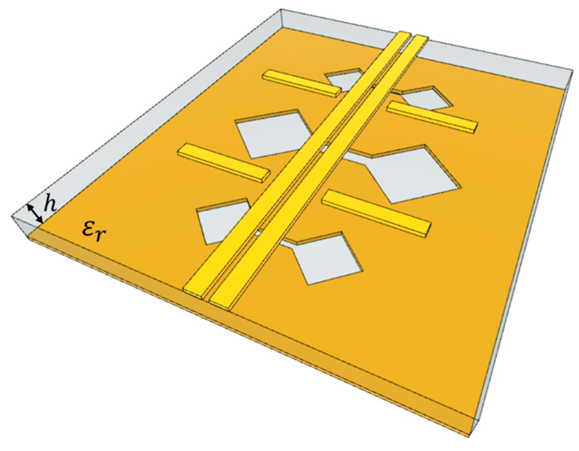
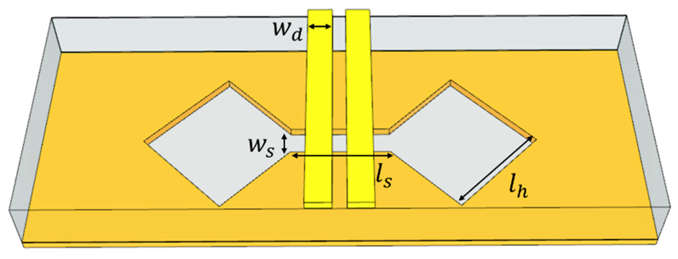
A perspective view of the proposed DS-DG CMR filter is shown in
Figure 1. On top of the substrate, a DL is laid out alongside with two pairs of gap-coupled stub (GCS) resonators placed between the DS-DG structures. On the bottom, three DS-DG structures with two different sizes of dumbbell-shaped apertures are laid out. The CMR filter is implemented with the Rogers RO4003C substrate (
,
h = 0.508 mm). The characteristic line impedance of the DL is 100 Ω, and the size of the CMR filter is 21.9 × 18.7 mm
2.
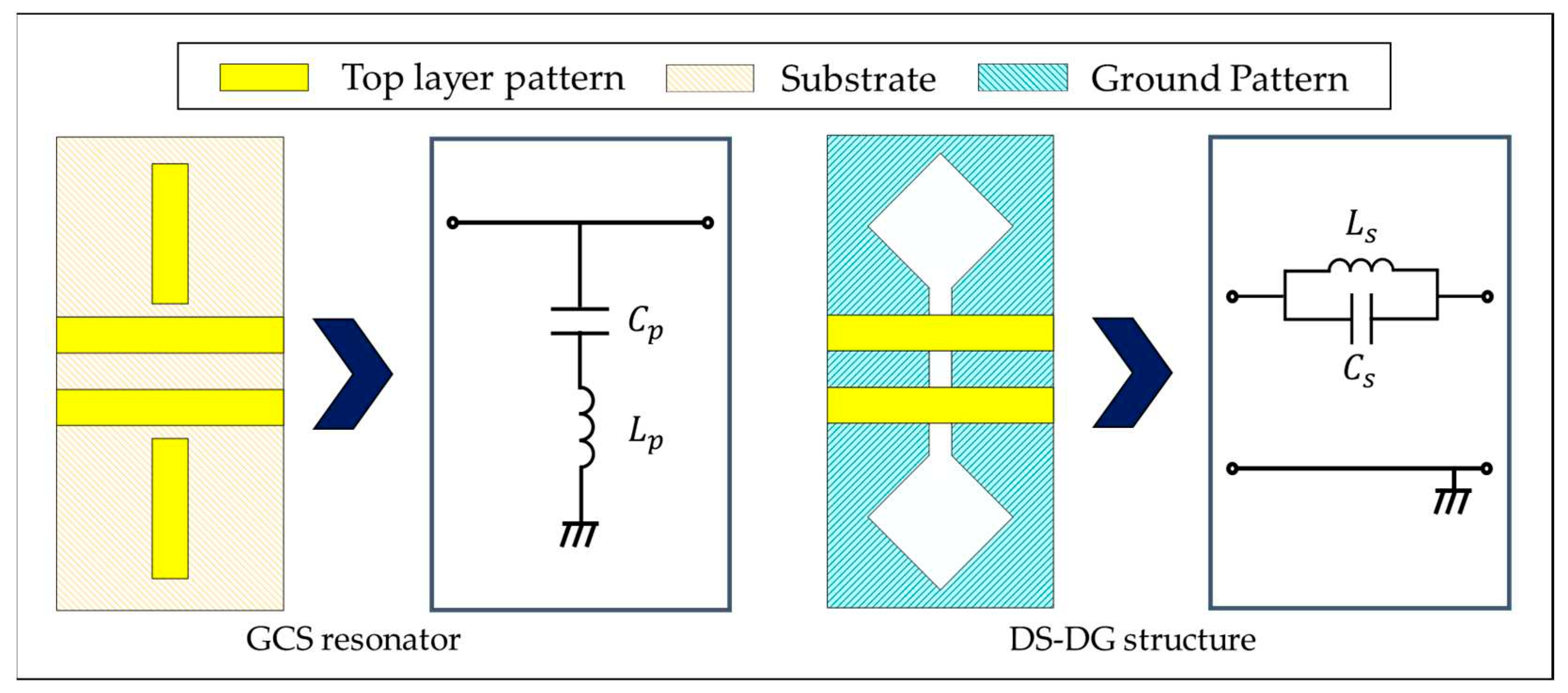
Simplified equivalent circuits for the DS-DG structure and the GCS resonator are shown in
Figure 2 [
10,
11]. The DS-DG structure can be represented by a parallel
LC-resonator series-connected on the line, and the GCS resonator can be expressed by a series
LC-resonator shunt-connected from the line.
For the proposed CMR filter, in order to obtain high rejection and selectivity, a 5
th-order Chebyshev band-stop filter is designed, and the element values of the low-pass prototype filter with 0.5 dB ripple are listed in
Table 1.
The values of
,
,
, and
of the CMR filter can be calculated from
using (1) and (2) with the required bandwidth (
) and center frequency (
).
With the proposed CMR filter, the center frequency is selected as 4.5 GHz with 4 GHz bandwidth (2.5 to 6.5 GHz).
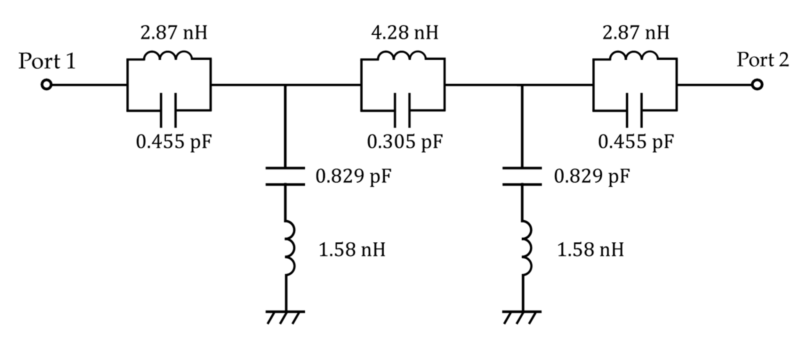
Figure 3 depicts an equivalent circuit for the 5
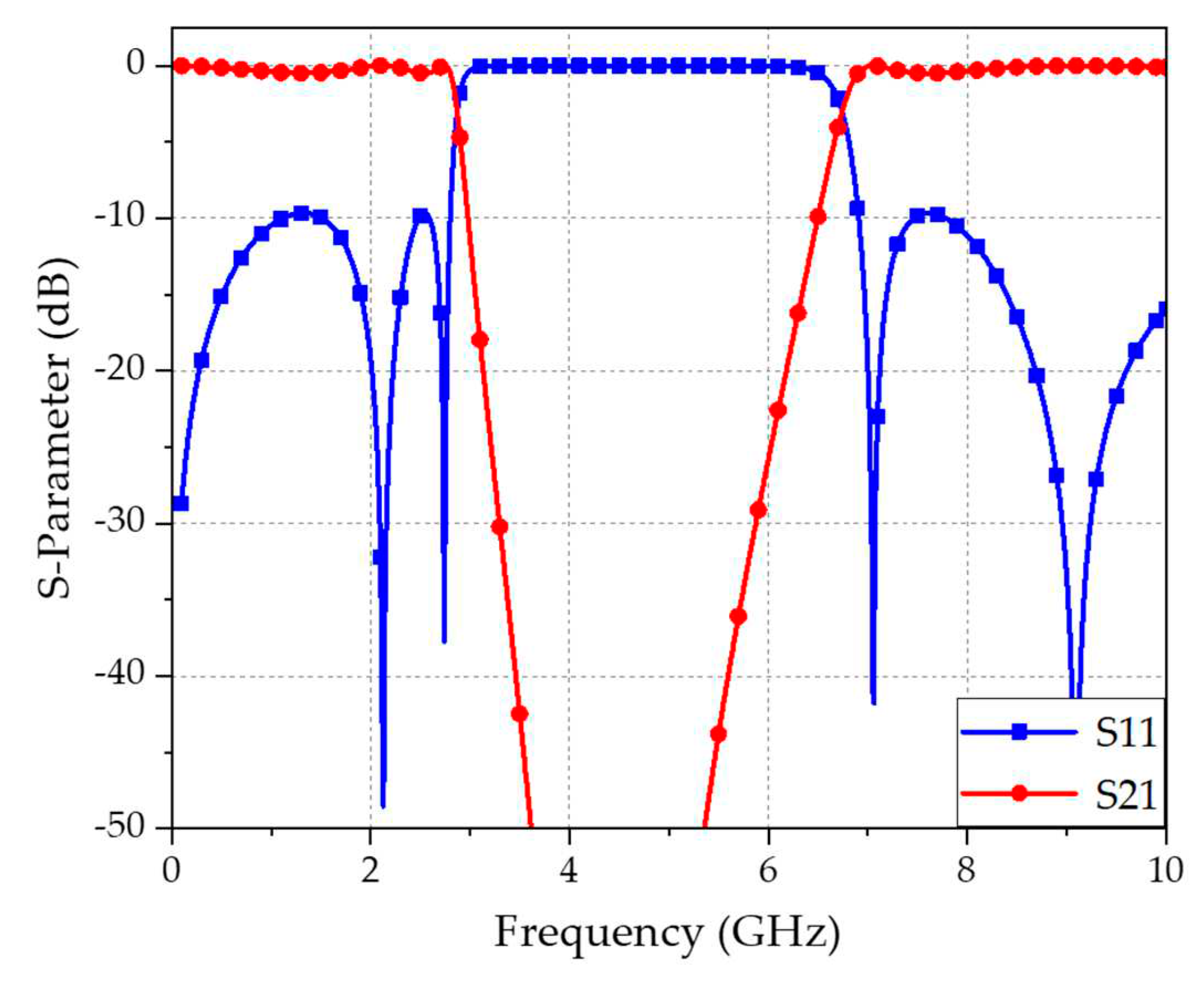
th-order Chebyshev band-stop filter to reject the common-mode components. The filter response with the filter parameters using ideal lumped elements is shown in
Figure 4. The center frequency is about 4.85 GHz, and the 3 dB-bandwidth is 4.1 GHz (2.8 to 6.9 GHz). Also, the bandwidth of 20 dB rejection is 3.2 GHz (3 to 6.2 GHz). There are two
S11 poles at 2.05 and 2.75 GHz, verifying a 5
th-order filter response.
2.2. DS-DG structure and its equivalent circuit model
A DS-DG structure used in the proposed CMR filter is illustrated with design parameters in
Figure 5. The dumbbell-shaped aperture is formed symmetrically across the DL on the bottom of the substrate. The diamond-shaped heads are connected with a dumbbell handle as a slot line. As a signal flows through the DL, an induced surface current flows along the periphery of the dumbbell-shaped aperture, equivalently represented by the corresponding inductance and capacitance.
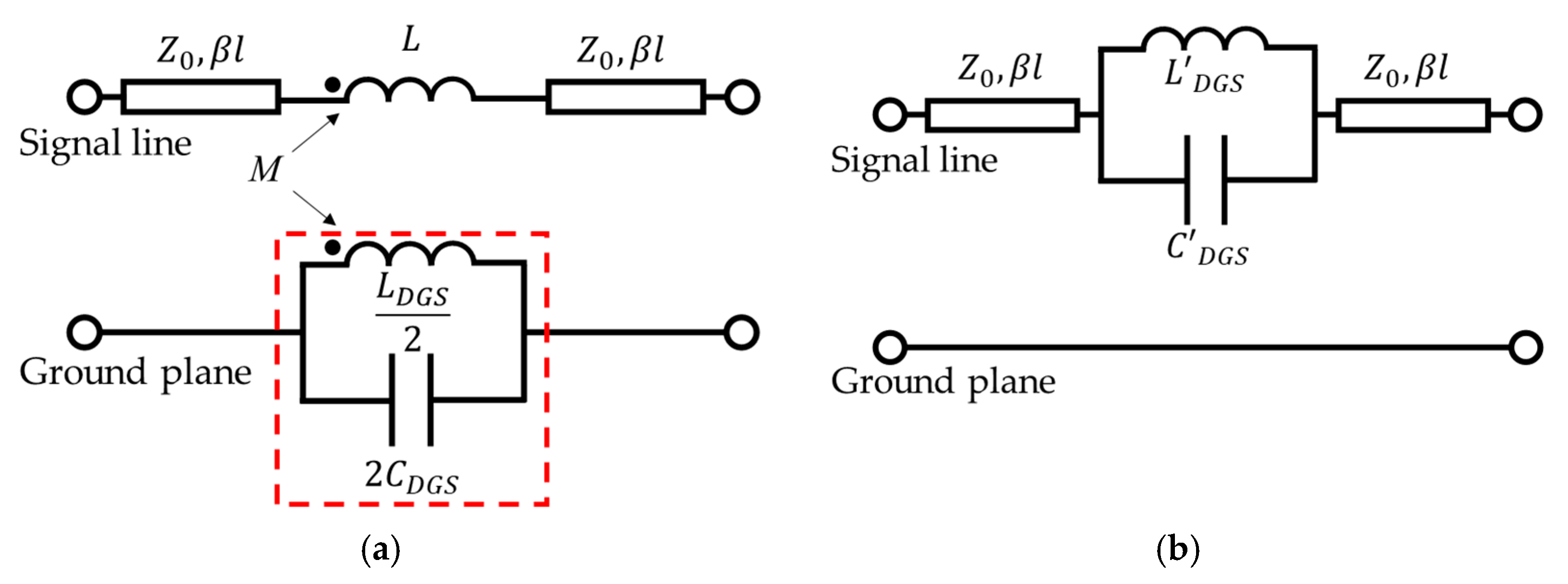
If a common-mode signal propagates along a DL and is encountered with a DS-DG structure, surface currents on the bottom substrate, circulating around the sides of the dumbbell-heads, are formed. Each extra current path on the ground plane induces an inductance value in addition to the capacitance value induced by the current path along the slot-line (i.e., dumbbell-handle) of the DS-DG structure. Therefore, an equivalent circuit model for a DS-DG structure can be configured as shown in
Figure 6a. The
LC-resonator (
) formed on the ground line can be transformed to an equivalent
LC-resonator (
) on the signal line using the mutual magnetic coupling with the inductance
L of the signal line, as shown in
Figure 6b.
The
C parameter value of the equivalent circuit in
Figure 6a can be obtained by using (3)
[7].
where
is the width of the dumbbell-handle, and
is the length of a side of the dumbbell-head. Also,
is the relative permittivity of a substrate. Eq. (3) approximates the capacitance of a slot-line of the DS-DG structure where
q’ in (3) is given as (4). In Eq. (3) the first term on the right-hand side represents the slot-line capacitance of the dumbbell-handle, and the second term is the capacitance of a dumbbell-head as an open slot-line.
In addition, the
L parameter value of the equivalent circuit in
Figure 6a can be obtained by using (5)
[12].
where
is the intrinsic impedance of an EM wave in free space, and
is the total length of the surface current circulating around the periphery of a dumbbell head (
). Also,
h is the substrate thickness, and
is the width of surface current circulating around the periphery of a dumbbell-head. Eq. (5) estimates the inductance of the circulating surface current around the sides of a dumbbell. For simplicity of the design process, the surface current width (
) is approximated as the width (
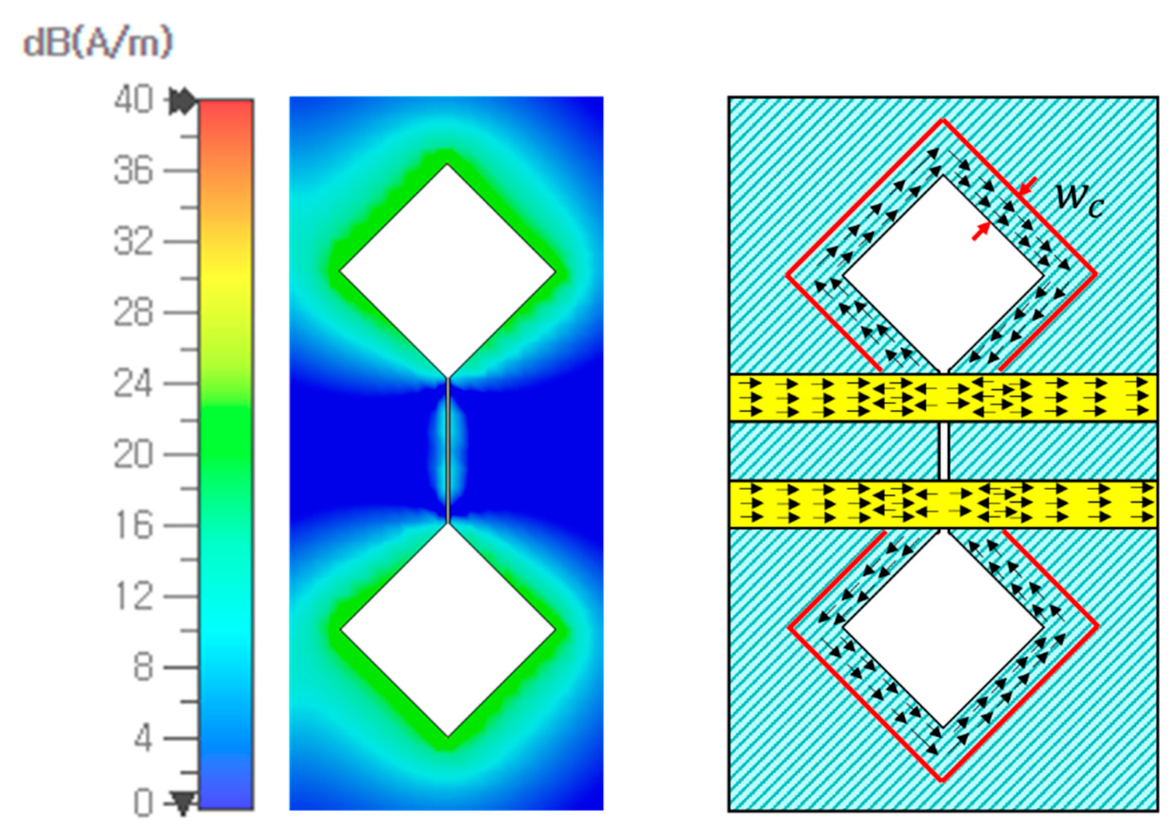
) of one signal line of the DL. With an EM simulation, as shown in
Figure 7, the current width of
corresponds to that of current density magnitude over 20 A/m. Also, it is found that a 10% change of
in (5) produces about a 2% change in resonance frequency, and the assumption of the surface current width as
consistently results in good agreement with the EM simulated results.
In order to transform the parallel
LC-resonator formed on the ground line to the one on the top signal line, as shown in
Figure 6b, the mutual magnetic coupling coefficient can be used: i.e.,
assuming
[
13]. Therefore, the final
L and
C values of the equivalent circuit in
Figure 6b can be expressed as (6) and (7) [
10,
13].
In order to prove the validity of assuming the surface current width as the width of the DL (
) along with other equivalent parameter values for the DS-DG structure, various DS-DG structures have been tested. For example, the transmission-zero frequency is designed as 4.5 GHz for various DS-DG structures, and the transmission-zero frequencies between the calculated (with the approximated formulas) and EM-simulated values (using the CST Microwave Studio) are compared in
Table 2. These resonant frequency values agree well within a 4.5% error, validating the above approximations.
2.3. GCS resonator and its equivalent circuit model
Using only an array of DS-DG structures on the bottom of the substrate, the complete Chebyshev band-stop filter cannot be attained since the shunt connections of series
LC resonators in between the DS-DG structures are missing. For example, a previous CMR filter used three DS-DG structures to implement a Chebyshev band-stop filter, and the obtained filter response was similar to that of a 3
rd-order Chebyshev filter [
8]. In this paper, the proposed CMR filter additionally utilizes two pairs of gap-coupled stub (GCS) resonators in between the DS-DG structures alongside of the DL, thus achieving a compact 5
th-order Chebyshev band-stop filter with three DS-DG structures and two pairs of GCS resonators.
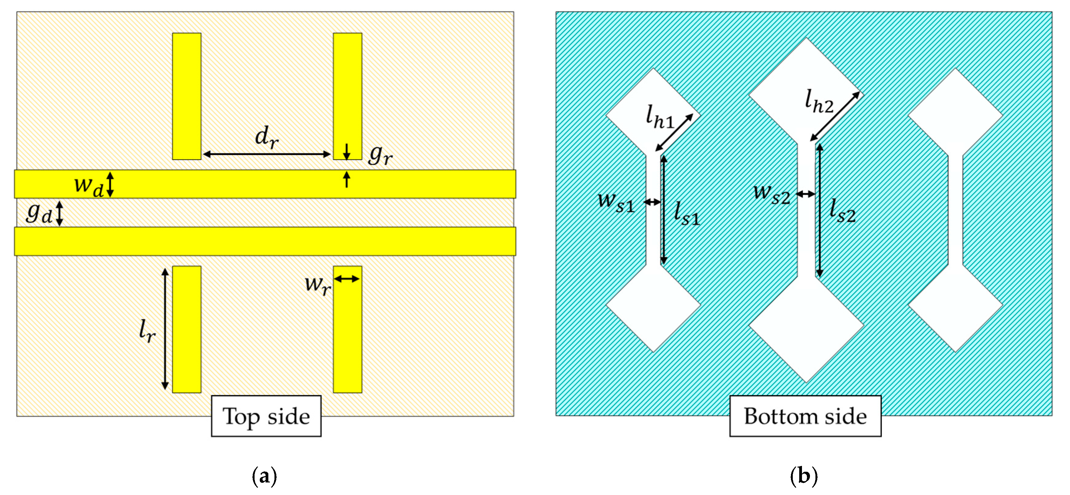
Figure 8a illustrates a configuration of two pairs of GCS resonators alongside of a DL. For the common-mode signal components propagating on the line, a GCS resonator works as a series
LC resonator shunt-connected to ground at each signal line of the DL. With the differential signals, the propagation property is dominantly determined by the linewidth and gap of the DL line, minimally affected by the surrounding structures such as the GCS resonator [
1]. The separation distance between the GCS resonators is chosen as
, and the length of the GCS resonator is
with a 50 Ω line impedance.
The equivalent capacitance and inductance of a GCS resonator are expressed in (8) and (9) [11, 14].
where
is the characteristic line impedance of one line of the DL,
is the element value of the low-pass prototype, and
is the normalized cutoff frequency of the low-pass prototype filter.
3. Simulations and Measurements
The top and bottom sides of the proposed CMR filter with the DS-DG structures and GCS resonators are illustrated in
Figure 8. The design parameters are listed in
Table 3. Also, in
Table 4, the
L and
C values of the proposed CMR filter for a 5
th-order Chebyshev band-stop filter are compared between the theoretical and calculated values with equivalent circuit models for the proposed CMR filter structure. The equivalent
L and
C values of DS-DG structures are accurate within 1.6% error on average, and those of the GCS resonator are accurate within 3.83% error on average. Therefore, the
L and
C values obtained by the theoretical formulas and the calculated values using the equivalent models agree well.
The proposed CMR filter with the DS-DG structures and GCS resonators is fabricated for measurements.
Figure 9 shows the top and bottom views of the proposed CMR filter.
The performance of the proposed CMR filter is measured with a four-port vector network analyzer (VNA: R&S ZNB40). As shown in
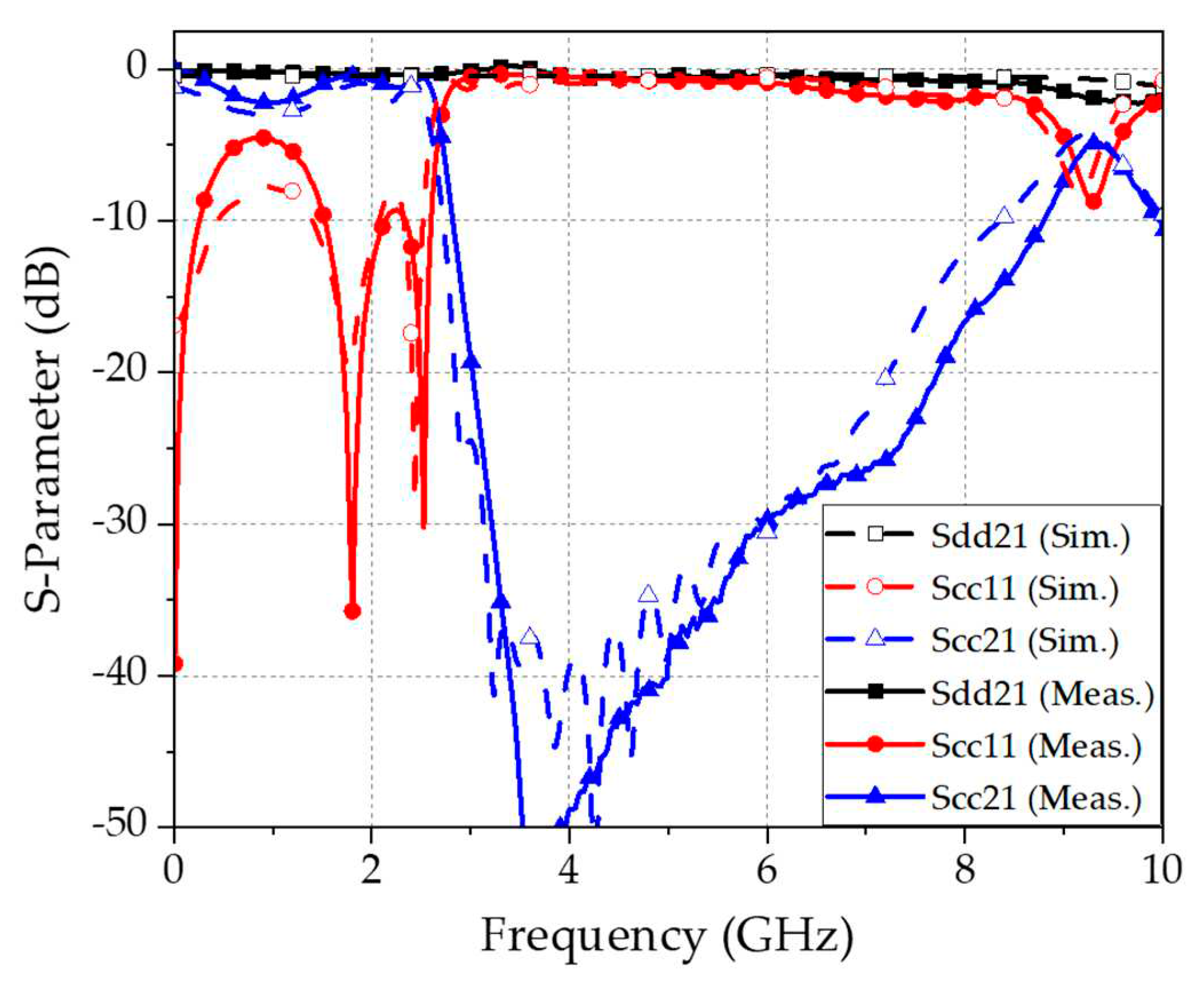
Figure 9a, the two signal lines of the DL at the launch and receive ends spread apart to form two 50 Ω microstrip lines for connection to the 4-port VNA. The measured 4-port S-parameters are configured as mixed-mode S-parameters to monitor separately the differential-mode and common-mode signals. The simulated and measured performances of the proposed CMR filter are shown in
Figure 10. The simulation is performed with a commercial 3D EM simulator (CST Microwave Studio). The simulated and measured S-parameter results agree very well. The implemented CMR filter provides the characteristics of a 5
th-order Chebyshev band-stop filter. For the differential signals, the insertion loss (Sdd
21) is less than 0.6 dB from DC to over 10 GHz. For the common-mode signal components, more than 20 dB rejection (Scc
21) is obtained for the frequency range of 3 to 7.8 GHz, with transmission zero frequencies at 1.8 and 2.45 GHz. Therefore, the proposed CMR filter with the DS-DG structures and GCS resonators provides very effective rejection of common-mode components at the same time with minimal effect on the differential-mode signals.
The performance comparison between the proposed CMR filter and the reported ones is given in
Table 5. The maximum insertion loss means the maximum insertion loss of the differential signal, the differential signal bandwidth is obtained with that less than 3 dB insertion loss, and the rejection bandwidth is obtained with that more than 20 dB rejection level. As can be seen, as compared with the previous reported results, the proposed CMR filter provides very good performance with wide rejection bandwidth (~90%) for the common-mode signals and low insertion loss (max. 0.6 dB) for the differential signals.
4. Conclusion
This paper proposes a simplified design approach for a compact and good-performing CMR filter with the DS-DG structures and GCS resonators. The proposed CMR filter design is based on equivalent circuit models for the DS-DG structures and GCS resonators. Previous design methods of DS-DG CMR filters heavily depended on tuning and optimization of the DG structures using 3D EM simulations. With this proposed CMR filter design, EM simulations are only used for performance verification. The proposed CMR filter structure is designed to effectively reject the common-mode signal components with minimal effect on the differential-mode signals. To validate this design approach, a 5th-order Chebyshev band-stop filter to reject the common-mode signals is designed, implemented, and measured. Simulated and measured performances agree very well. The implemented CMR filter provides the insertion loss (Sdd21) of less than 0.6 dB from DC to over 10 GHz for the differential signals, and more than 20 dB rejection for the frequency range of 3-7.8 GHz for the common-mode signal components. The proposed compact, high-performing CMR filter can be applied to improve the signal integrity of high-speed digital signals on PCBs.
Author Contributions
Conceptualization, J.S.C. and B.C.M.; methodology, J.S.C.; validation, J.S.C. and K.W.K.; formal analysis, J.S.C.; investigation, J.S.C., B.C.M. and M.J.K.; resources, B.C.M., M.J.K. and J.S.C.; data curation, J.S.C., M.J.K. and S.K.; writing—original draft preparation, J.S.C. and K.W.K.; writing—review and editing, B.C.M., K.W.K. and H.C.C.; visualization, J.S.C.; supervision, K.W.K. and H.C.C.; project administration, K.W.K.; funding acquisition, K.W.K. All authors have read and agreed to the published version of the manuscript.
Funding
This research was supported in part by the National Research and Development Program through the National Research Foundation of Korea (NRF) funded by the Ministry of Education (No. NRF-2022R1I1A3064460) and in part by the BK21 FOUR project funded by the Ministry of Education (No. 4199990113966).
Data Availability Statement
Not applicable.
Acknowledgments
This research was supported in part by the National Research and Development Program through the National Research Foundation of Korea (NRF) funded by the Ministry of Education (No. NRF-2022R1I1A3064460) and in part by the BK21 FOUR project funded by the Ministry of Education (No. 4199990113966).
Conflicts of Interest
The authors declare no conflict of interest.
References
- Martín, F.; Zhu, L.; Medina, F.; Hong, J.S. Balanced Microwave Filters; John Wiley & Sons: Hoboken, New Jersey, 2018. [Google Scholar]
- Henry, W.O. Electromagnetic Compatibility Engineering; John Wiley & Sons, 2009. [Google Scholar]
- Kumar, A.; Kartikeyan, V.M. Microstrip filter with defected ground structure: a close perspective. International Journal of Microwave and Wireless Technologies 2013, 5, 589–602. [Google Scholar] [CrossRef]
- Jordi, N.; Armando, F.P.; Miguel, D.S.; Francisco, M.; Jesus, M.; Francisco, M.; Ferran, M. Common-mode suppression in microstrip differential lines by means of complementary split ring resonators: theory and applications. IEEE Trans. Microw. Theory Tech. 2012, 60. [Google Scholar] [CrossRef]
- Zhu, H.R.; Mao, J.F. An ultra-wideband common-mode suppression filter based on S-DBCSRR for high-speed differential signals. IEEE Microw. Wireless Components Lett. 2015, 25. [Google Scholar] [CrossRef]
- Wu, S.J.; Tsai, C.H.; Wu, T.L.; Tatsuo, I. A novel wideband common-mode suppression filter for gigahertz differential signals using coupled patterned ground structure. IEEE Trans. Microw. Theory Tech. 2009, 57. [Google Scholar] [CrossRef]
- Liu, W.T.; Tsai, C.H.; Han, T.W.; Wu, T.L. An embedded common-mode suppression filter for GHz differential signals using periodic defected ground plane. IEEE Microw. Wireless Components Lett. 2008, 18. [Google Scholar] [CrossRef]
- Yang, D.H.; Yeh, C.I.; Jeffrey, S.F.; Cheng, J.C.; Chin, K.S.; Chiu, H.C.; Xiao, J.K. SLL similarity filling factor design for Chebyshev modulated dumbbell DGS low pass filters. IEEE Asia Pacific Microwave Conference, Singapore, 7-10 Dec. 2009; pp. 1–4. [Google Scholar]
- Chang, I.S.; Lee, B.S. Design of defected ground structures for harmonics control for active microstrip antenna. IEEE Antennas Propagation Society International Symposium, San Antonio, Texas, 16-21 June 2002; pp. 852–855. [Google Scholar]
- Su, L.; Paris, V.; Jonathan, M.E.; Ferran, M. Discussion and analysis of dumbbell defect-ground-structure (DB-DGS) resonators for sensing applications from a circuit theory perspective. Sensors 2021, 21, 8334. [Google Scholar] [CrossRef] [PubMed]
- Vijay, S.; Mohammad, H. Effective blood bank management system based on chipless RFID. IEEE Indian Conference on Antennas and Propagation, Ahmedabad, India, 19-22 Dec. 2019; pp. 1–4. [Google Scholar]
- Frederick, W.G. Inductance calculations: working formulas and tables; Courier Corporation: New York, U.S.A., 2004. [Google Scholar]
- Woo, D.J.; Lee, T.K. An equivalent circuit model for a dumbbell-shaped DGS microstrip line. Journal of Electromagnetic Engineering and Science 2014, 14, 415–418. [Google Scholar] [CrossRef]
- Hong, J.S. Microstrip filters for RF/microwave applications; John Wiley & Sons: Hoboken, New Jersey, 2011; pp. 169–175. [Google Scholar]
|
Disclaimer/Publisher’s Note: The statements, opinions and data contained in all publications are solely those of the individual author(s) and contributor(s) and not of MDPI and/or the editor(s). MDPI and/or the editor(s) disclaim responsibility for any injury to people or property resulting from any ideas, methods, instructions or products referred to in the content. |
© 2023 by the authors. Licensee MDPI, Basel, Switzerland. This article is an open access article distributed under the terms and conditions of the Creative Commons Attribution (CC BY) license (http://creativecommons.org/licenses/by/4.0/).
