Introduction
Electrically conductive adhesive (ECA)/sealant design can achieve different properties and cost even if the same polymer matrix is used. As adhesives, they are expected to have moderate to high tensile and shear strengths and they are typically used to replace or reinforce lead soldering and conductive metal components. Sealants or flexible adhesives typically have lower strength but higher deformability while maintaining their electrical conductivity. They are used in defense, aerospace, automotive and appliance industries and can have a variety of rubber and elastomer materials as the primary matrix material. These matrix materials provide resistance to excessive flow and exhibit viscoelastic behavior. Tack can be achieved by additions of tackifiers such as rosin esters, mineral fillers and/or petroleum derivatives [
1].
Metallic conductive fillers impart electrical conductivity to polymer-based conductive adhesives if their volume fraction is above their percolation threshold as illustrated in references [
1,
2,
3,
4,
5,
6,
7,
8].
Non-conductive or low-conduction fillers are coated with a conductive coating to induce electrical conductivity in polymer-based composites. For example, Dilsiz et al. [
9] used the chemical reduction method to coat nickel filaments and hematite and magnetite spindle type particles with silver. In that process, reducing agent type, reactant concentration and reaction time all affected silver coating morphology and the conductivity of the coated particles. Similarly, Aussawasathien and Sancaktar [
10] electrospun and then silver coated polyacrylonitrile-based carbon nanofibers to study their properties and surface morphologies.
Aussawasathien and Sancaktar [
11] also used sol-gel processing and electrospinning to fabricate poly(vinyl pyrrolidone) (PVP)-nickel acetate (Ni(CH
3COO)
2·4H
2O) composite fibers which were then converted to nickel oxide (NiO) nanofibers. High temperature (700 °C) calcination of the PVP/Ni acetate composite for 10 h was used for this purpose. Reduction to NiO nanofibers was accomplished at 400 °C subsequently using hydrogen gas (H
2) under inert condition to produce metallic nickel (Ni) nanofibers, which were chemically coated with silver (Ag) nanoparticles. This process provided enhanced electrical property and prevented surface oxidation of the Ni nanofibers.
Polymers have been known as insulators. However, doping can convert polymers into electrically conductive materials. A π-conjugated system formed by the carbon and nitrogen Pz orbitals overlaps and the presence of C
6 rings (i.e., polyaniline) leads to electrical conduction in homogeneous (unfilled) polymers [
12,
13]. The doping of the conjugated backbone molecules in polyacetylene, poly(p-phenylene), poly(p-phenylene vinylene), poly(p-phenylene sulfide), polyaniline, polypyrrole, and polythiophene with electron acceptors leads to delocalized π electrons and electrical conductivity. Electrically conductive polymers prepared in this fashion still pose many problems with respect to controllable conductivity, environmental stability and mechanical properties [
14]. Using ammonium persulphate oxidizing agent in aqueous HCl solution, Sancaktar and Liu [
15] produced emeraldine salt (ES; doped PANI), which they used in homogeneous powder as well as in (ES filler – nitrocellulose) adhesive composite forms to study the relationships among electrical resistivity, morphology, viscoelastic and chemical behaviors. Their results showed percolation threshold at ~30% vol of ES powder.
Effect of Pressure
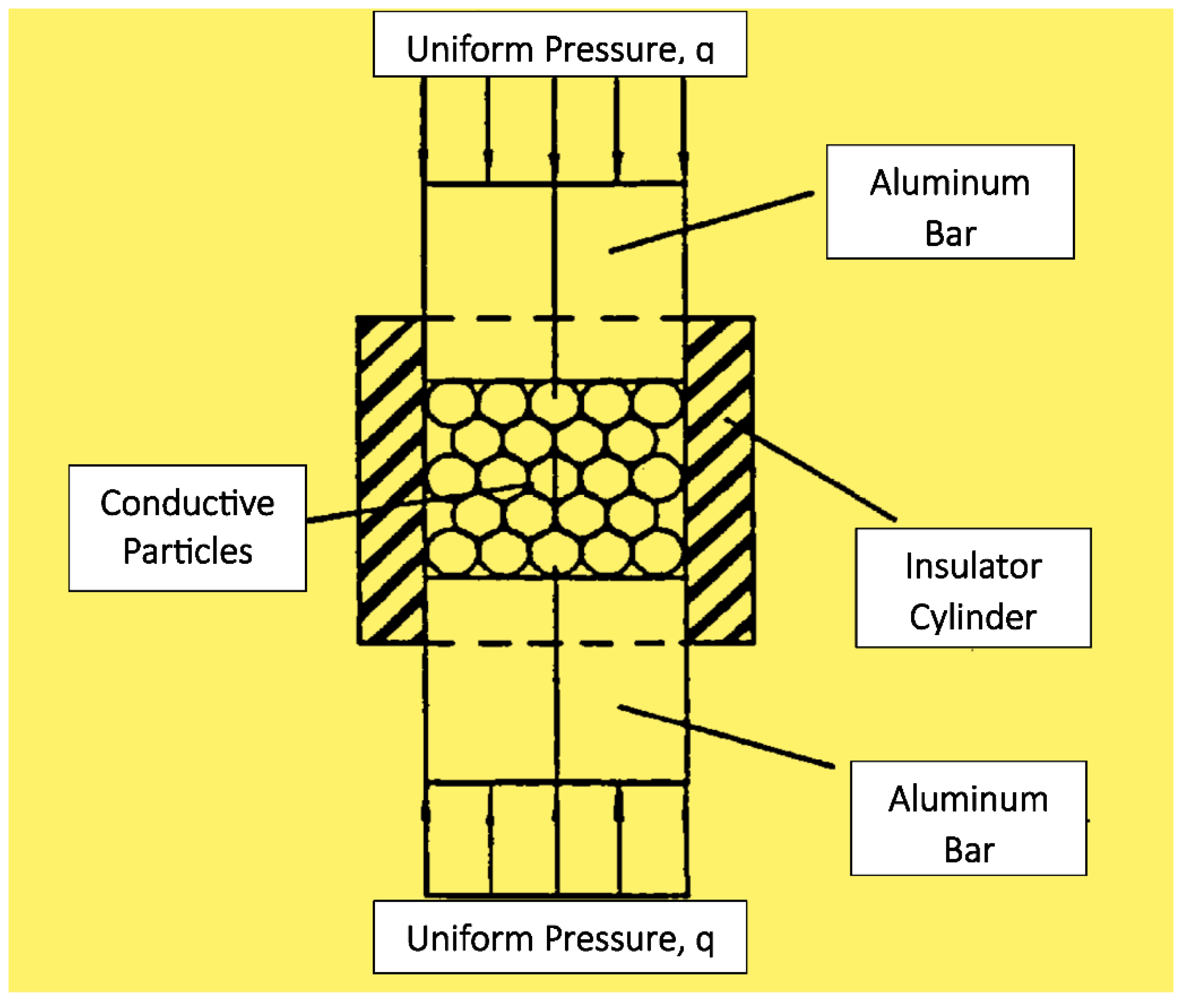
For the ES filler study summarized above, a hollow cylinder fitted with conducting plungers (
Figure 1) was used to show that the resistivity of ES powder reached the lowest level rapidly with the application of a pressure cycle, but it increased at a relatively slow but varied rate as the cycles of compressive force incrementally increased with each cycle starting from zero pressure. This process involved 82.19% compaction strain initially, followed by 15.17% plastic strain exhibited by the ES powder. This behavior was discussed based on the unique main chain π-conjugation necessary for electron flow, and the importance of the polymer’s intrinsic viscoelasticity on its electrical conduction behavior was revealed.
Assuming spherical particles in
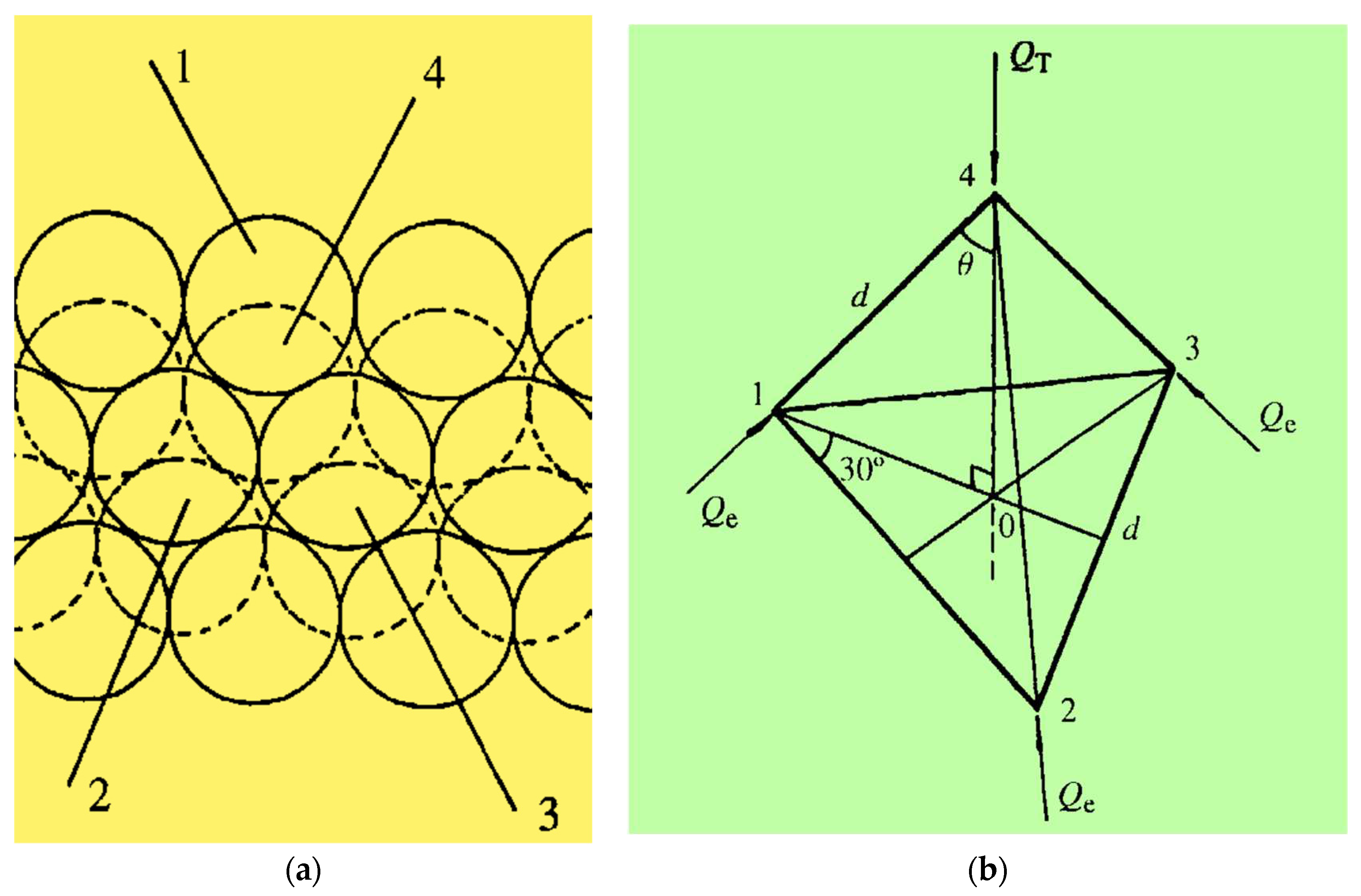
Figure 1, and except for the top and bottom layers, there are twelve contact points for each particle in the cylinder. If we consider particles 4 (in top layer) and 1, 2, 3 (in layer below the top;
Figure 2a), the force vector Q
T (applied on individual particles) will be balanced by Q
e (the interparticle contact force;
Figure 2b). The Y-axis is at θ = 35.3° to line 1- 4.
A total external pressure of q (N/m
2) is applied on the top layer of our cylindrical compression device, and Q
T is given by:
where, r = particle radius, f = packing factor (f = 0.906 for 2-D hexagonal packing).
Therefore, the contact force Q
e is given by:
The metal sphere particles will deform with the application of Q
e, creating a (circular) contact area, which has the radius, a [
16]:
where, υ = Poisson's ratio, E = Young's modulus of particles.
By substituting Q
e in Equation (4), we get
Constriction and tunnel resistances make up the contact resistance:
where, ρ
1 and ρ
2 are (spherical) particle resistivities and,
In Equation (8), ρσ (Ω - m2) = tunnel resistivity.
The contact resistance can now be written as:
For the case, ρ
1 = ρ
2 = ρ, we have:
In Equation (10), ρ
σ depends on the width (s) of the tunnel and its relative permitivity (ε
r); work functions (φ
1 and φ
2) for electron emission from the particles into the tunnel and the applied voltage (V). ρ
σ is approximately independent of the voltage when the tunnel width is small (s < 15A) [
17]. For the case, φ
1 = φ
2, we have:
The contact resistance model developed by Sancaktar and Wei [
6] revealed that the resistance doesn't change significantly if s < 4 Å, but will increase significantly with increasing tunnel width when s > 4 Å.
Equation (10) shows that the contact resistance is inversely proportional to the contact area, and Equation (5) shows that the contact area is directly proportional to the external (applied) pressure. The contact resistance is directly proportional to the tunnel resistivity.
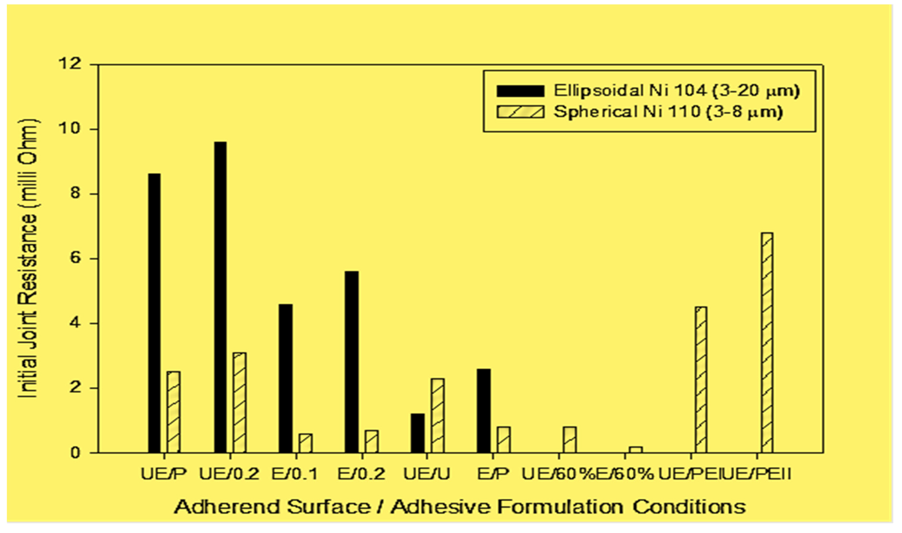
Figure 3 shows the (initial) joint resistance for single lap joints with unetched substrates (UE) bonded using two different conductive adhesive formulations (35% by volume Ni 104 and Ni 110; see
Figure 3 insert) under two different pressures (binder clips - low pressure, and C-clamps – high pressure; P or U) [
18]. The adhesive matrix used was Epon 830 with 170 - 225 Poise viscosity (Shell, Houston, TX) crosslinked using 11% diethylenetriamine (DETA) (Shell).
Figure 3 shows that higher bonding pressure (clamped specimens) results in lower joint resistance, especially with ellipsoidal Ni 104 (3–20 μm), possibly due to squeeze flow of the neat resin and more efficient particle contact under high pressure. The resin squeeze flow is likely to be more effective when larger particles (i.e., Ni 104 vs. Ni 110) are used.
Basan and Sancaktar [
19] used silicone rubber (SE64, Dow Chemical) and N234 carbon black (CB) in 40, 50, 60, 70, 80, 90 ve 100 phr (per hundred rubber) proportions to prepare highly deformable conductive composites compounded (C.W. Brabender Instruments Inc., Compounder, South Hackensack, NJ) along with vulcanizing agent at 0.3 rps and room temperature for 20 min. The compound was press-cured at 28 MPa pressure and 100
oC over 35 min period by a Carver (Wabash, IN) Model 3912 hydraulic press to obtain 2 mm thick conductive sheets. Subsequent to cure, the highly deformable silicon rubber composite’s resistivity decreased over a period of time, and the percolation threshold depended on the applied compressive load. Basan and Sancaktar [
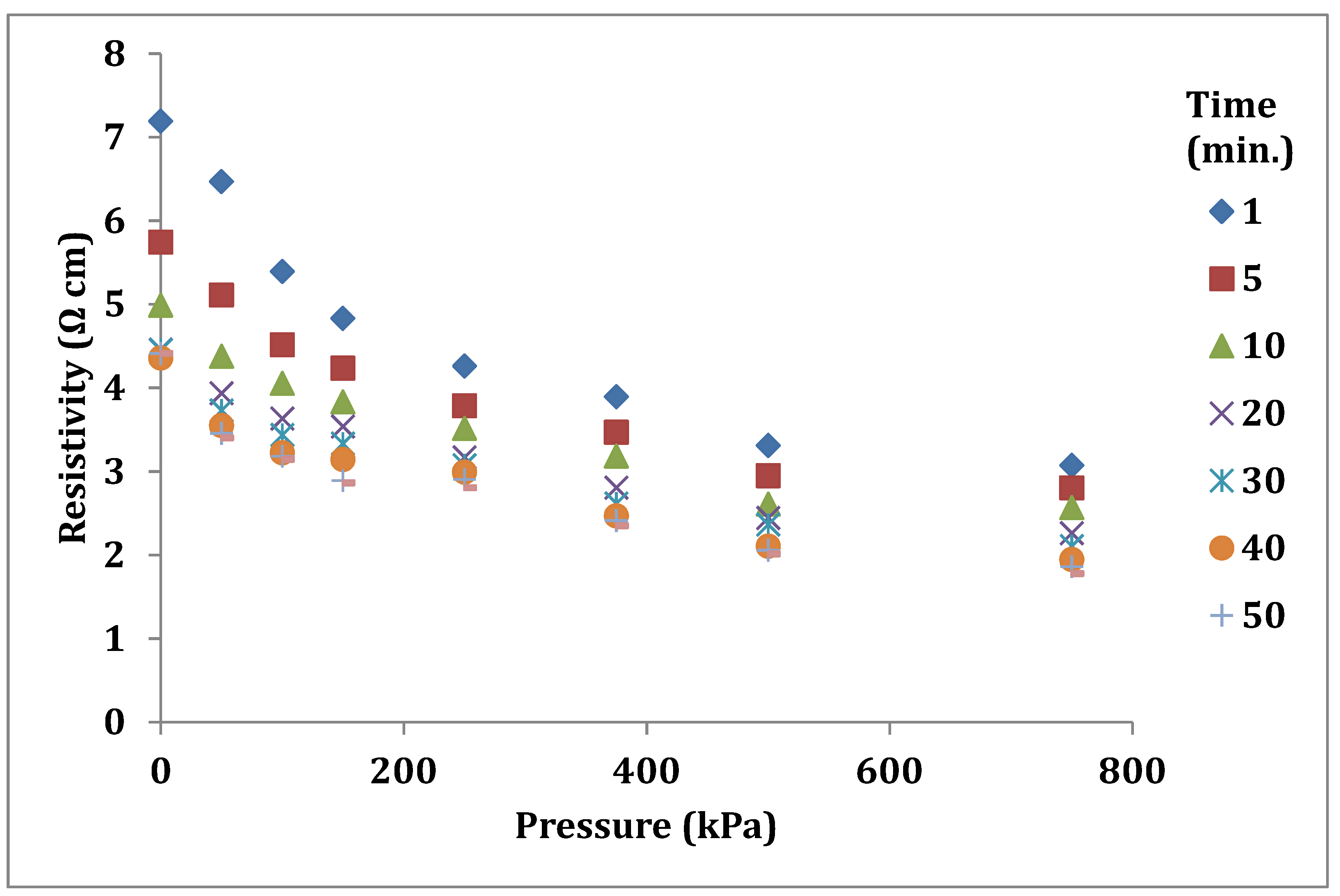
19] evaluated the rate dependence of the composites’ resistivity by measuring the storage moduli, G´ under compression and showed that the stiffness decreased with strain levels leading to lower resistivity at higher strains (higher pressures). This is clearly seen in
Figure 4 by comparing the resistivity magnitudes at low and high pressure levels. Furthermore, they noted that increases in frequency resulted in higher G´ values, meaning that higher pressure rates should result in lower resistivity. This behavior can be varified by noting the decrease in slopes (for example time = 1 min.) of individual curves at increasing pressures in
Figure 4. These two characteristics define the typical asymptotically decreasing resistivity versus pressure behavior observed in
Figure 4. These findings show that the loading rate and the strain level can be used as conductivity actuation parameters in electronic/electrical devices by using CB-filled SG composites.
Effect of Conductive Filler Volume Fraction
Wei and Sancaktar [
5] showed that the 2-D and 3-D conduction path factor values approached each other with increasing volume fraction, eventually merging at 50 % vol, and the volume resistivity, ρ, is given by:
where D = diameter of spherical filler, R
s = contact resistance, Φ = volume fraction of fillers, and m = average contact number. Based on Equation (16), 3-D to 2-D transition results in 82% increase in resistivity level for the Φ = 0.35 case. With the lower filler particles volume fraction of Φ = 25% (Ag/Ni powder mixture case shown in
Table 1) a 141 % increase in ECA resistivity (from 3.05 to 7.34 mΩ cm) is observed due to 3-D to 2-D transition.
We note that, Gomatam and Sancaktar [
18] observed increases in their single lap joint resistivity values when the adhesive thickness was increased from 100 to 200 µm (
Figure 3). The author attributes this increase to the absence of adequate bonding pressure as thickness control shims were used with bonding pressure induced by medium size paper clamps. In the absence of high bonding pressure, adequate squeeze flow was not achieved, and the volume fraction of the non-conductive epoxy resin remained high with increases in tunnel resistivity and conductive path length. This result illustrates the importance of pressure in conductivity of these types of adhesives.
Equation (16) reveals that the filled adhesive resistivity may be inversely proportional to an (n) power of the volume fraction, Φ, leading to an equation of the type,
proposed to be used to represent resistivity - volume fraction data [
2].
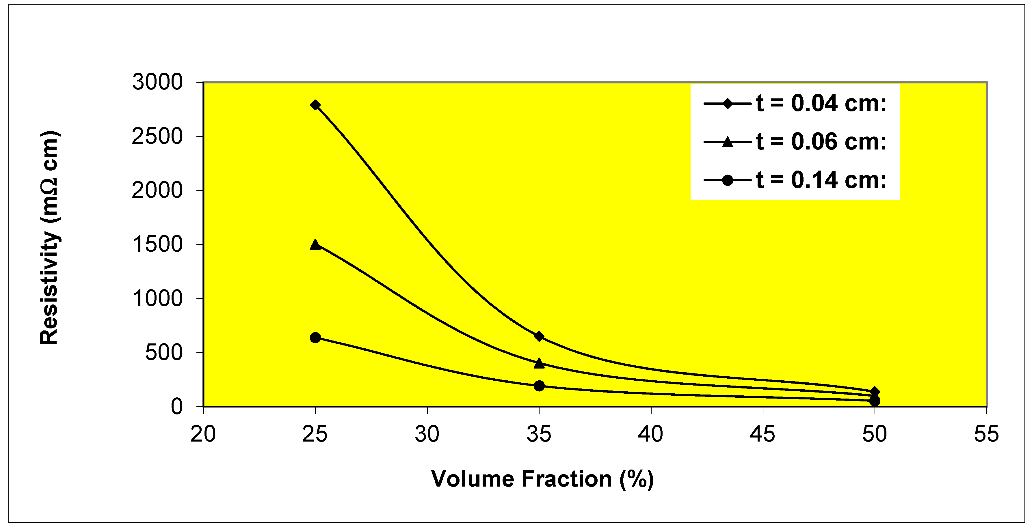
Figure 6 presents results which demonstrate the behavior described by Equation (17). The specimens were prepared by manual casting of different-thickness uncured adhesive films in molds of different thickness and cured in an oven at 60
oC for 3 hours as recommended by the supplier (Shell). The Ni particles were etched with 10% Hydrochloric acid (HCl) to remove the surface oxide layer by covering with the etching solution and occasional mixing for 5 minutes, followed by rinsing with distilled water and drying in an oven at 120
oC.
In discussions above, increases in ECA thickness resulted in reduced resistivity levels in the form of negative exponential decaying functions, described by Bai and Sancaktar [
2] with the equation:
where t = adhesive thickness (cm), and the parameters a, b, c are used to fit the experimental data to Equation (18) with parameter a representing the asymptotic resistivity w.r.t. ECA film thickness. The parameters a, b, c are functions Φ, and A and n are functions of t [
2]. Therefore, Equations (17) and (18) can be equated:
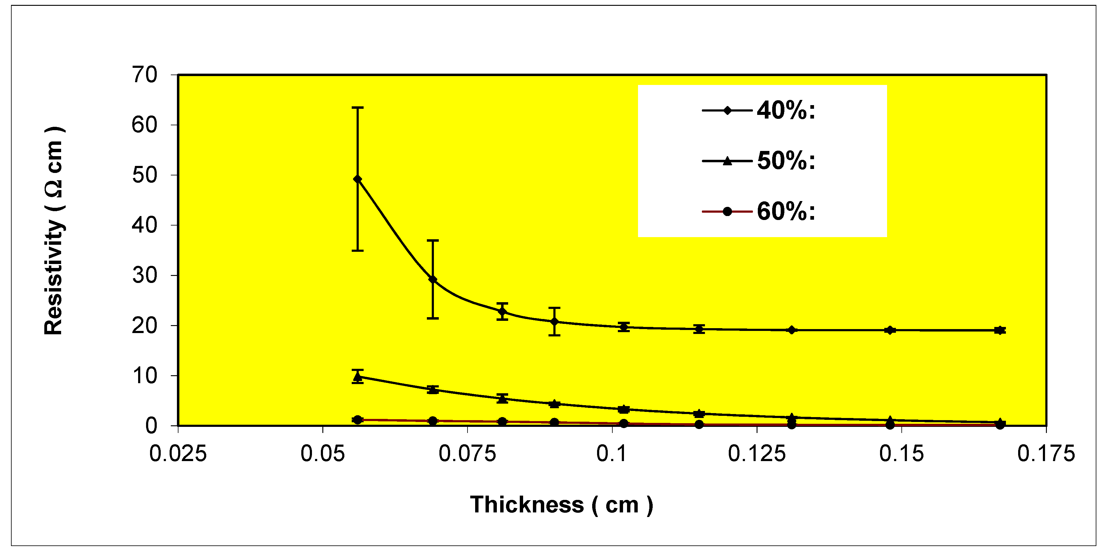
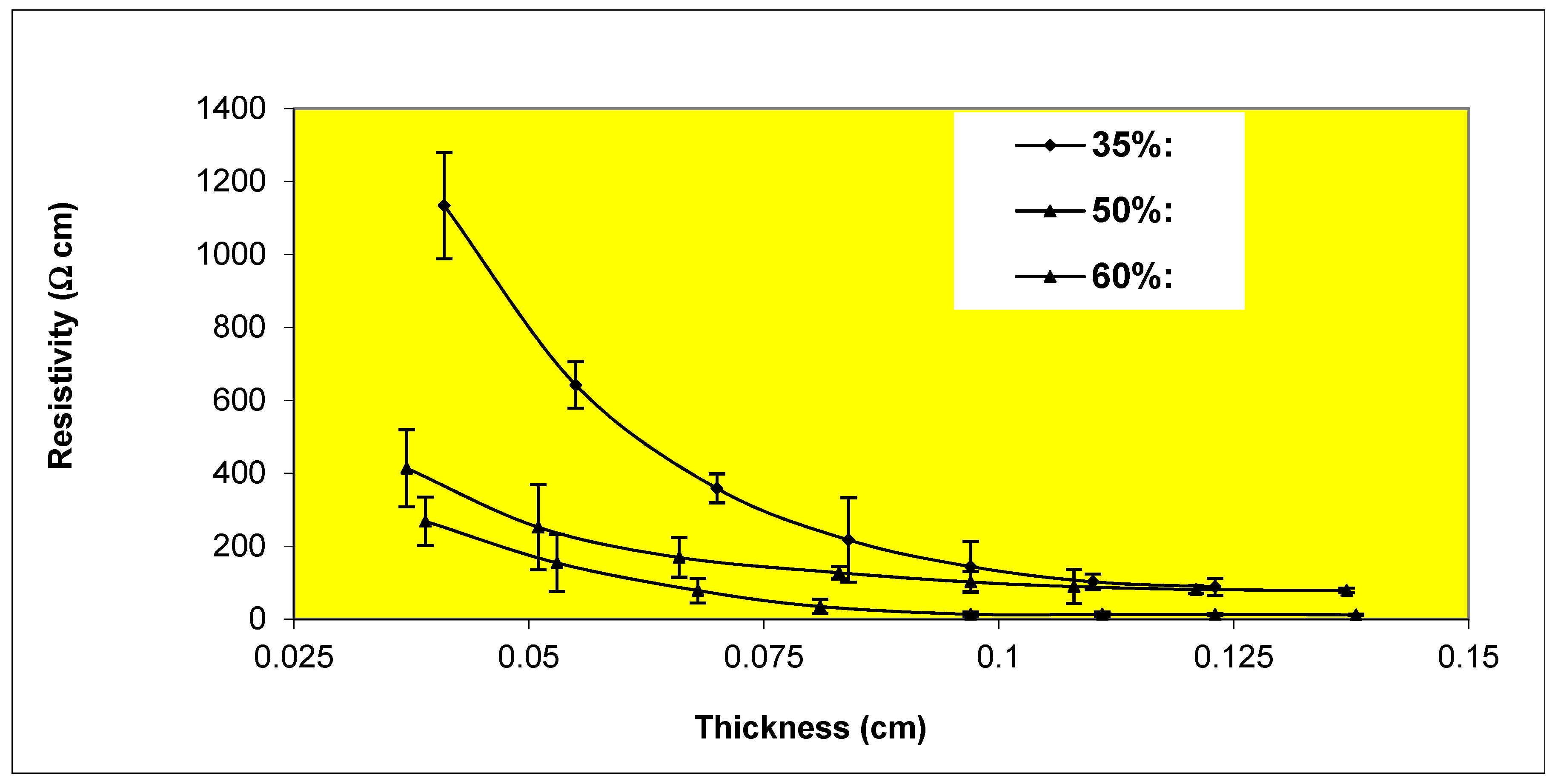
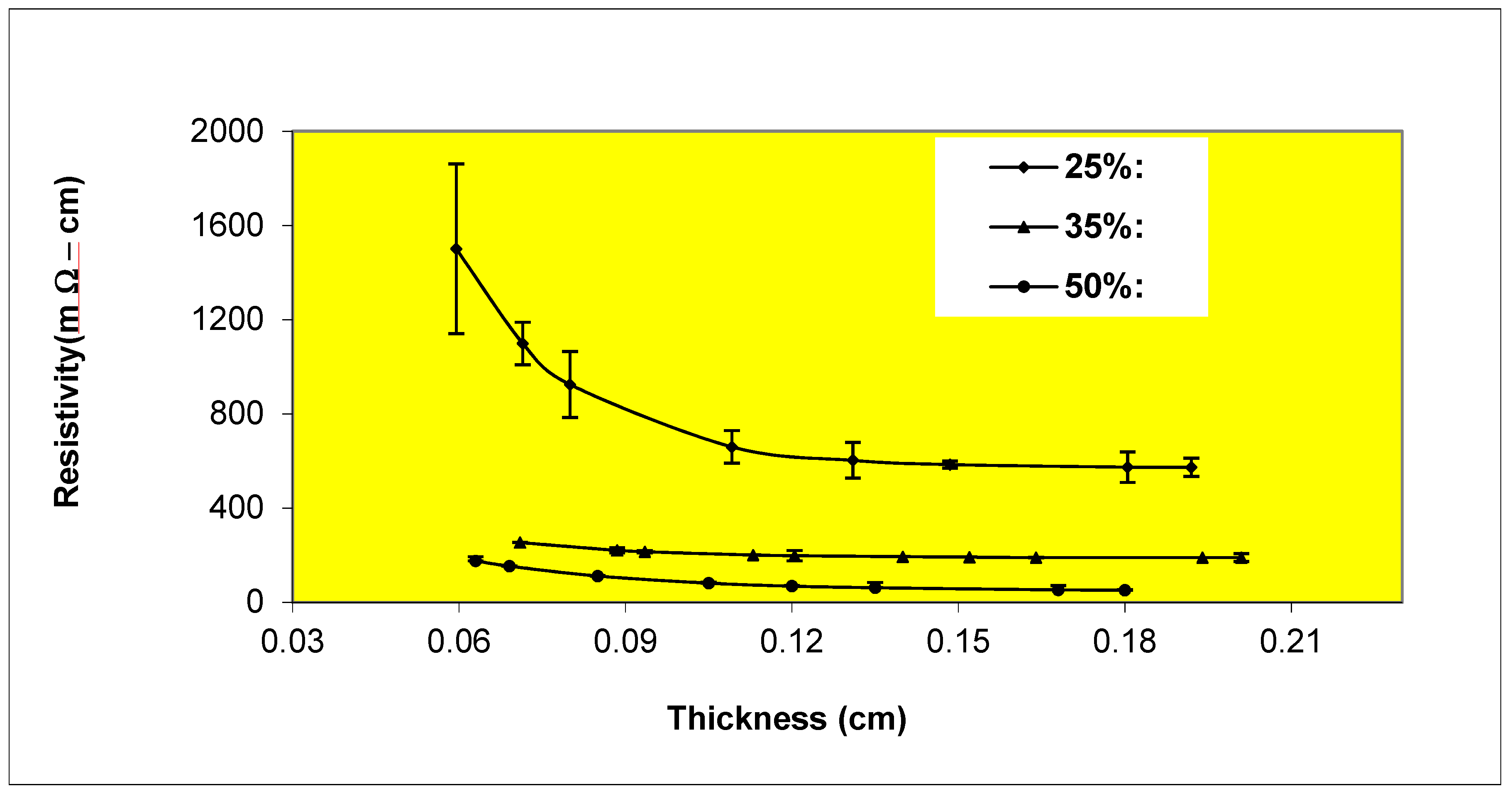
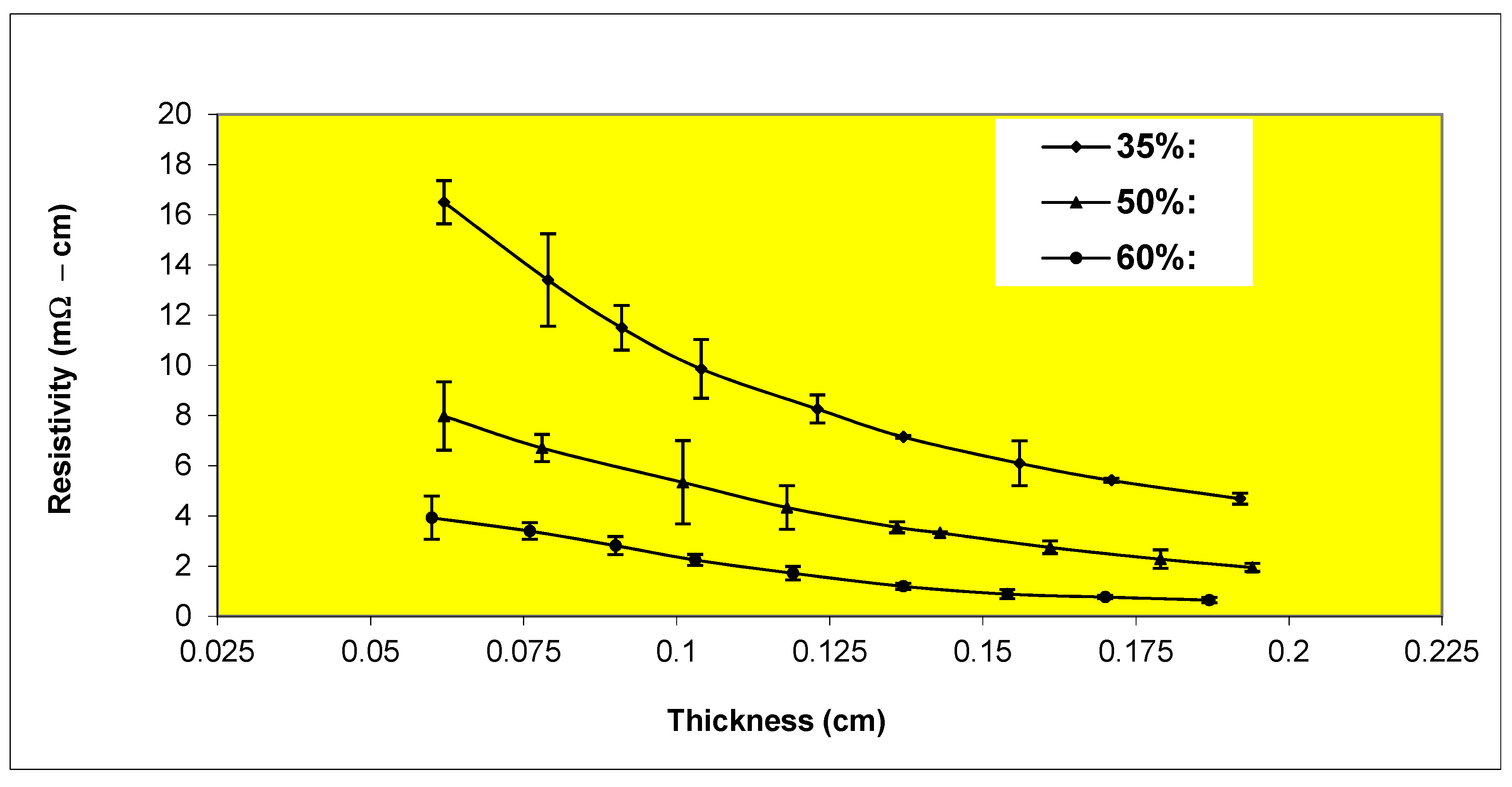
Figure 7,
Figure 8,
Figure 9,
Figure 10 and
Figure 11 present results which demonstrate the behavior described by Equation (19). The specimens were prepared by casting adhesive films manually with the thickness of the film as an experimental variable as described above in conjunction with
Figure 6. The Ni and copper particles were etched with 10% HCl and 20% Phosphoric acid, respectively, to remove the surface oxide layer by covering with the etching solution and occasional mixing for 5 minutes, followed by rinsing with distilled water and drying in an oven at 120
oC.
Nanocomposite Conductive Adhesives
Nanocomposite conductive adhesives have become popular with the emergence of “nanotechnology”. Sancaktar and Kuznicki [
21] used Cloisites 30B supplied by Southern Clay Products (Gonzales, TX) to reinforce epoxy resins. Cloisites 30B is clay organically modified with methyl, tallow, bis-2-hydroxyethyl, quaternary ammonium to facilitate wetting of approximately 1nm thick clay layers by the liquid epoxy Epon 815C and Epon 830 resins (Shell, Houston, Texas). Epon 815C is a low viscosity epoxy resin (5 - 7 Poise viscosity) which is a mixture of 86.4% DGEBPA epoxy and 13.6% monofunctional butyl glycidyl ether (Heloxy Modifier 61, reactive diluent, Shell, Houston TX). Based on the mechanical properties, the optimal level of nano clay loading was around 0.5% wt for Epon 815C and 2% wt for Epon 830. The addition of nanoclay resulted in mechanical property improvements with the 815C system in terms of, elastic modulus and maximum and yield stresses. Nanocomposite toughness and stress whitening increased at 1% indicating a high mechanical interaction between the clay particles reducing shear sliding and, thus, shear-yielding. Nanocomposite formation in the 830 resin was hindered by its higher viscosity (170 - 225 Poise) resulting in improvements only in yield stress with some improvement in maximum stress.
Kim and Reneker [
22] reported that 10 phr nanofiber addition to styrene-butadiene rubber provided 10-fold increase in Young’s modulus in comparison to the pure material. Sancaktar and Aussawasathien [
23] also reported on mechanical properties of nanofibers and their composites. Aussawasathien and Sancaktar [
24] showed that the high thermal conductivity, high fiber aspect ratio and the resulting highly interconnected network of carbon nanofiber (CNF) mats caused the rate of cure reaction for CNF mat-epoxy nanocomposites to be higher than that for the neat epoxy resin, especially at low cure temperatures. It is well known that the cure conditions (time and temperature) affect the mechanical and interfacial properties of filled/reinforced thermoset resins [
25,
26,
27,
28]. The carbon nanofiber (CNF) mats rendered the epoxy based adhesive composite electrically conductive. The maximum influence of the CNF mats on cure rate was observed at specific values of cure temperature and time with the mat-effect becoming insignificant at high temperature - long time curing. With the addition of the CNF mat to epoxy resin, its cure behavior involving heat flow rate, reaction rate, conversion and residual heat were all enhanced, especially during the initial stages of cure. Thus, the ECA nanocomposite required lower activation energy for cure, which was achieved in shorter times. It should be noted however that, the cure reaction may be retarded due to the diffusion hindering effect of the CNF mat, especially at high CNF mat loading, which may lead to low crosslinking density. Kamal’s model [
29] was used successfully to predict the cure kinetics of CNF mat-epoxy nanocomposites.
Qian et al. [
30] reported up to 25% increase in the composite strength with the addition of nanotubes. Multiwall nanotubes (MWNTs) have weak inter-shell interactions [
31] which limit their applications, while single wall nanotubes (SWCNTs) present processing and cost challenges. Thus, alternative nanofillers including graphite nanoplatelets and graphitic carbon nanofibers (GCNFs) which can be functionalized using additives to provide strong interfacial bonds with the matrix can also impart conductivity in nanocomposites.
Sub-micron size fillers with large specific surface area can form highly interconnected network thus enhancing the mechanical properties of their polymer matrix [
8,
23,
32]. These characteristics are also expected to enhance electrical conduction in polymer matrix (nano)composites since the total resistance between the conductive (nano)particles is inversely proportional to the contact area (Equation 10).
Table 2 presents volume resistivity of epoxy ECA’s filled with different types of conductive nanofibers as reported by Aussawasathien and Sancaktar [
10]. Obviously, using Ni nanofiber in mat form can reduce the conductive path factor considerably.
Adherend Surface / Adhesive Formulation Effects
Gomatam and Sancaktar used Epon 830 epoxy filled with Ni 104 (3-8 µm) and Ni 110 (as received: 3-20 µm, and HCl-etched), (Degusa©, Dusseldorf, Germany) particles to prepare conductive adhesives [
18,
33]. In order to prepare the conductive adhesives, two different particle volume fractions were used, namely, 35% by volume [
5], and 60% vol (Ni powder density is 2 g/cm
3 [
34]). For etching, the Ni 110 particles were covered with 10% HCl (5 ml HCl, and 45 ml distilled water) solution for 3 minutes (designated UE/PEI) or 5 minutes (designated UE/PEII), with occasional mixing followed by rinsing with distilled water and drying in an oven at 120
oC. The single lap adherend samples had 25.4 mm overlap length with the resin applied to the bonding sides using a spatula. Medium size paper clamps were used to pressurize the adherends for bonding. Different bonding pressures were also applied using paper clips and C-clamps, with C-clamps providing maximum bonding pressure, Different adhesive bond-line thicknesses were also incorporated using shims in the bonding jig. In order to avoid adhesive fillet formation, any extra resin flash was removed from the sides of the overlap. The samples were cured in an oven at 121
oC for 2 hours and cooled at room temperature.
Figure 3 shows the initial joint resistance of single lap joints with different steel adherend surface conditions (unetched and etched; UE or E), ECA formulation (Ni 104, Ni 110, 3 and 5 minute-etched Ni 110, 35%, and 60% by volume), adhesive bond line thickness (BLT), 0.1 mm or 0.2 mm (0.1, or 0.2), and bonding pressures by binder clips, and C-clamps (P or U). We note that use of ellipsoidal Ni 104 particles results in lower joint conductivity in comparison to spherical Ni 110 nickel particles. When the adherend bonding surfaces are etched resulting in the topographical parameters of Ra = 1.65 µm, Rz = 14.3 µm, and Rmax = 20.97 µm (conditions indicated by E / 0.1 and E/0.2), the joint resistance is reduced by 85% for joints bonded with Ni 110 filled ECA, which has smaller particles (3-8 µm), rather than Ni 104 filled ECA with larger particles (3-20 µm). Obviously, the smaller particles can easily get into the adherend surface crevices, providing better electrical connection between the joint substrates. Gomatam and Sancaktar also reported that with Ni 110 adhesive formulation filled at 35 phr, the reduction in the ultimate displacement values were larger for the unetched adherend joints in comparison to the etched joints when the test machine crosshead rate was increased from 1 to 100 mm/min (interfacial failures are more likely at higher rates), indicating the importance of proper mechanical anchoring of the particles with the etched surface. On the other hand, increasing the particle volume fraction in order to reduce the joint resistance (
Figure 3) causes significant reductions in the ultimate displacement and failure load values for both etched and unetched specimens as shown in
Table 3.
Gomatam and Sancaktar [
18] also showed that increasing the etching time from 3 to 5 minutes for the Ni 110 particles resulted in approximately 60% increase in joint resistance. Pressure-dependent conduction behaviors of various etched (with 10% HCl) and as received particles were studied by Sancaktar, and Dilsiz in the absence of resin [
3]. They reported 96%, and 89% reductions in the bulk resistances of the same dry nickel powder (no resin) measured under 0.7 MPa, and 7 MPa compression, respectively. On the other hand, the observation of higher joint resistance after increased particle etching time by Gomatam and Sancaktar resulted due to increased wetting enhancing adhesive layer formation around the particles by etching of the particles. Such increased adhesive layer formation causes an increase in the tunneling resistance within the ECA as well as its conduction to the substrate surfaces. This argument was substantiated by the authors [
18] with the fact that the joint deformation and strength improved with 5 min–etched Ni particles, clearly indicating improved particle wetting and adhesion. This result is illustrated in
Table 4.
Electrical conductivity of ECA’s as well as the associated behaviors such as heat conduction and mechanical behavior (strength, rigidity, deformation and viscoelastic behavior, all of which may be affected by moisture ingression [
21,
35,
36,
37]) are also affected by adhesive viscosity and thickness, filler shape, size and volume fraction, substrate and filler surface treatment and the applied pressure (during bonding and during conduction). In order to gain insight into electrical and mechanical performance of electronically conductive adhesives (used in electronics), Sancaktar et al. [
8] used (single) overlap joints made with C151 copper alloy copper substrates (0.1% of zirconium in pure copper) with four different types of plating, gold (Au), tin (Sn), nickel (Ni) and a palladium-nickel (PdNi) alloy. The substrates had the following dimensions, width = 0.25 mm, thickness = 0.25 mm, length = 9.5 mm, bonded with an overlap range of 0.54 - 1.1 mm, using 0.06 to 0.11 mm thick silver-filled thermosetting ECA. The adhesive was cured at 150
oC for 30 minutes. Some samples were also immersed in deionized water at 70
oC for 24 hours. Their results revealed the following conclusions: Conduction and the joint strength strongly depended on the conditions at the adhesive/substrate interphase. Conductivity and joint (interfacial) strength were inversely related in newly-bonded joints. This result, again, illustrates that increased adhesive layer formation on substrate surfaces (coated with Au) causes increases in the tunneling resistance between the substrate surface and its adjacent ECA particles due to the Au affinity by the resin. This argument was substantiated by the work of Gomatam and Sancaktar [
18] with the fact that the joint deformation and strength behaviors improved when (5 min-etched Ni particles were used, clearly indicating improved particle wetting and adhesion (
Table 4).
Even though the joint strength was reduced after 254 hours of water immersion, hydration did not significantly increase the joint resistivity [
8] due to efficient metal-to-metal contact within the conductive joint. This finding was further supported when it was observed that oxidation on nickel coating caused the joint resistance to increase significantly when compared with PdNi, Au and Sn coated substrates.
Gomatam and Sancaktar [
38] prepared stainless steel (304) and aluminum adherends treated using silane coupling, grit blasting and plasma treatment to fabricate single-lap joints to be tested under various environmental and fatigue conditions. The joints were bonded using Ablebond MA-2 ECA (Ablestik Laboratories, Rancho Dominguez, CA). The joint fatigue life and the cyclic creep displacements increased substantially with silane-treated substrates at higher loads, even though the increase in the fatigue life was marginal and the increase in creep displacements were smaller at higher temperatures. Plasma treatment and grit blasting substantially improved the fatigue life, while silane treatment of the grit-blasted surfaces did not provide any additional benefits in terms of fatigue life. This observation further illustrated that mechanical adhesion (anchoring) can sufficiently improve interfacial adhesion. Moisture ingression was reduced significantly with grit blasting preventing interfacial failures. It is interesting to note that silane treatment of the grit-blasted surfaces did not provide reductions in moisture intake.
With their fatigue experiments, Gomatam and Sancaktar also determined that increases in temperature and humidity levels [
39,
40,
41] and reductions in the cyclic frequency of the ECA joints at ambient environmental condition resulted in substantial reductions in fatigue life [
42]. We note that, as the cyclic frequency of the applied load is decreased, the exposure time for the propagating crack to high loads is longer. Furthermore, as the cyclic waveform was changed from sinusoidal to square, the fatigue life decreased.
Method of Application
Zhou and Sancaktar [
43] observed resin migration before cure and under static pressure for (Epon 830 and Epon 815C) epoxy-based ECA’s filled with 50% wt etched Ni (3 μm Ni 102 flakes, as received from AEE, Micron Metals, Inc., NJ; and etched with 10% HCl). Use of lower viscosity (5 - 7 Poise) Epon 815C/Ni (etched) resulted in electrical conductivity gradients and unstable capillary flow during and after injection process. As the shear rate increased, the plunger force and its oscillation frequency increased. The flow was stabilized at 75 % wt Ni concentration, while it could be stabilized at 62.7% wt when the 170 - 225 Poise viscosity Epon 830 resin was used as the binder. Stable capillary flow could also be obtained using 80 nm Ni nanopowders (Inframat Advanced Materials LLC, CT) even though filler agglomerate formation was observed [
43].
Zhou and Sancaktar [
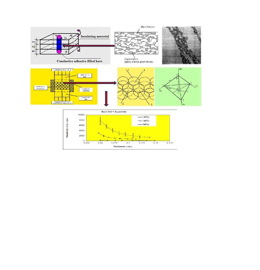
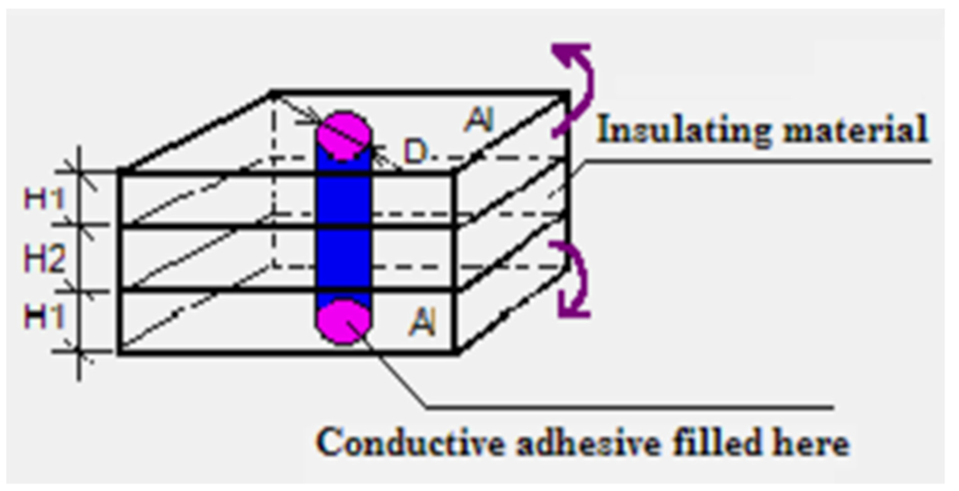
44] considered electrical resistance of multilayer hole-structure with ECA-filled holes connecting nonconductive layers to investigate the relation between the structure geometry and conduction using conductive (Al) plates covering the nonconductive Garolite sheets (McMaster-Carr, Aurora, OH) representing circuit boards (
Figure 12). As expected, adhesive - adherend interfacial contact and the ECA resistivity dominated conduction in the prototype shown in
Figure 12. They proposed Equation (20) to empirically represent the contact resistance (R
c Ω) as function of the hole diameter (D mm) and plate thickness (H mm), using Epon 830/Ni (60 % wt) /DETA ECA after cure, using regression analysis (R
2 = 0.955):
Sancaktar and Dilsiz [
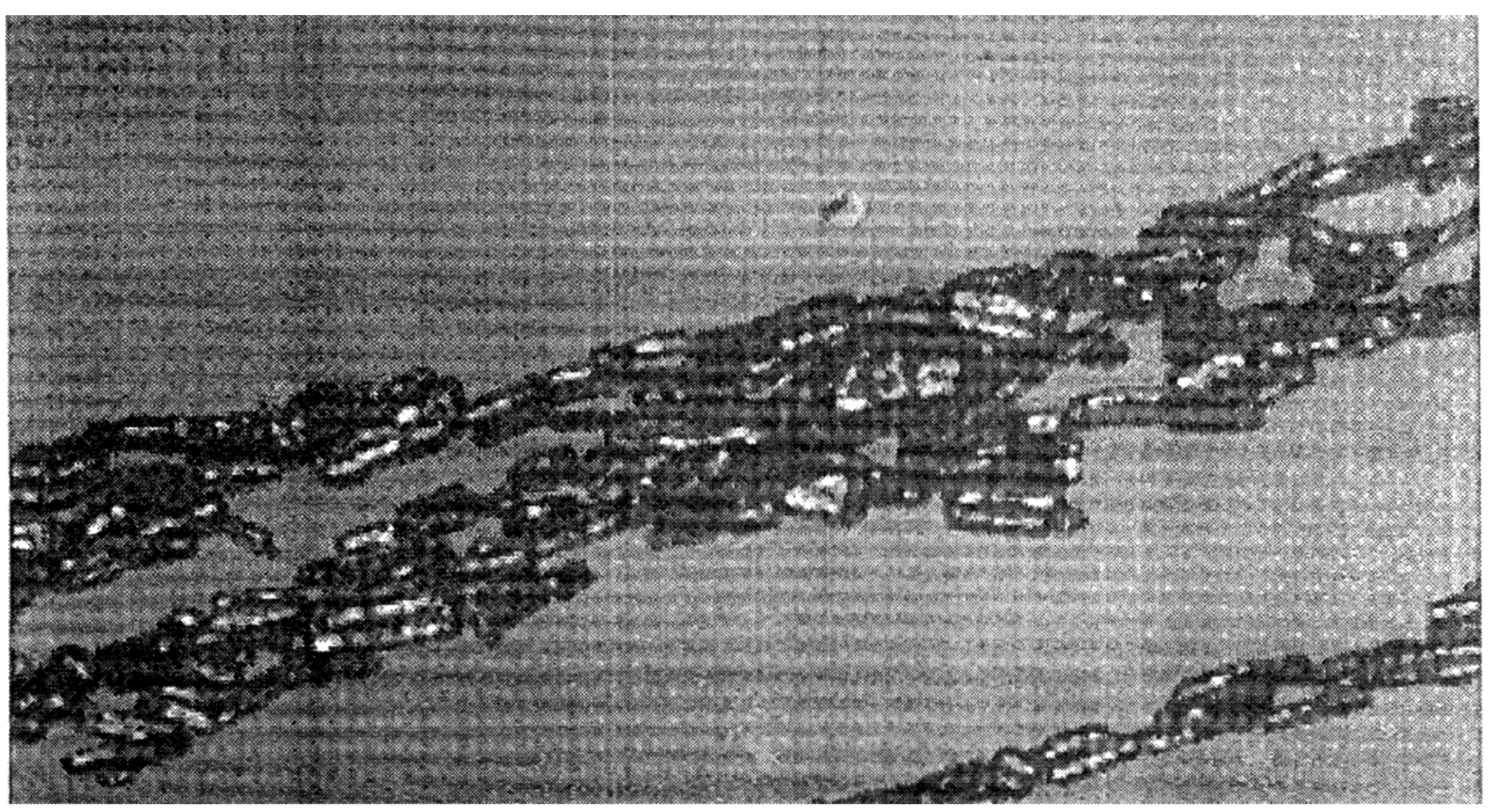
44] magnetically aligned conductive nickel particles (10% vol; 20 µm D, 160 µm long filaments, as received or chopped for 60 min; 3- 7 µm powder; 1-5 /µm or 3 µm flakes) in Epon 815 epoxy matrix to fabricate anisotropically (directionally) conductive adhesives. Anisotropic conductivity was achieved in the direction of the 1000-7500 Oe magnetic field applied to the ECA film for 2 min (
Figure 13).
Their results revealed that the size and shape of the magnetic Ni particles used, their oxidation condition and volume fraction, as well as the resin viscosity, all affected the magnetically created directional electrical properties of the fabricated ECA’s. Using filament and flake shaped magnetic particles with high aspect ratios helped to produce magnetic moments and the magnetic alignment process. Some filament particles were chopped using a blender and acquired a bowed shape, thus reducing directional resistance by increasing the number of particle contacts and reducing the conductive path length, S. Use of flakes produced a similar effect. Thicker films required higher intensities of magnetic field. Plane isotropic (3-D) to anisotropic directional (1-D) electric conduction transition in the adhesive films was approximately 15% vol with the nickel powders used and 5% vol with the nickel fibers used.
Figure 1.
Device used to study pressure effect on conductive particles’ resistivity.
Figure 1.
Device used to study pressure effect on conductive particles’ resistivity.
Figure 2.
a) Hexagonal packing of spherical particles (dotted particles are in top layers). b) Contact force, Qe, free body diagram.
Figure 2.
a) Hexagonal packing of spherical particles (dotted particles are in top layers). b) Contact force, Qe, free body diagram.
Figure 3.
Initial joint resistance with various conductive single lap joint substrate surface, adhesive formulation, thickness, and applied pressure conditions. Unetched and etched substrates (UE or E); formulation of the conductive adhesive: Ni 104, Ni 110 (3 and 5 min etched), Ni 110 35%, and 60% by volume; adhesive bondline thickness (BLT): 0.1 mm or 0.2 mm (0.1, or 0.2); bonding pressures: C-clamps – high pressure; binder clips - low pressure (U or P).
Figure 4.
The variation of 70 phr SG/CB composite resistivity with pressure and time.
Figure 4.
The variation of 70 phr SG/CB composite resistivity with pressure and time.
Figure 5.
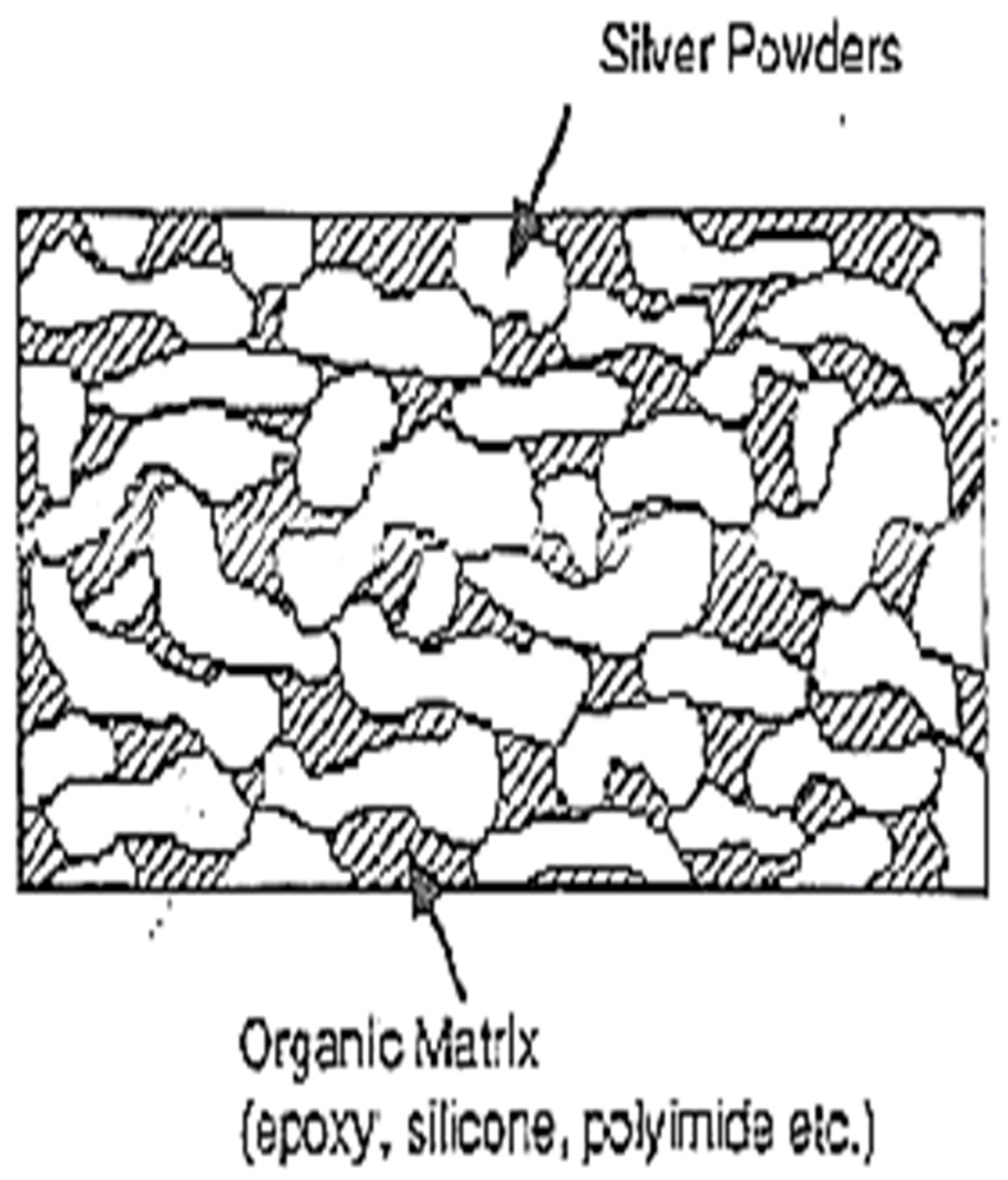
Representation of conductive path development in silver flake powders.
Figure 5.
Representation of conductive path development in silver flake powders.
Figure 6.
Variation of resistivity with volume fraction and thickness (t) for Epon 830/etched nickel flake ECA’s.
Figure 6.
Variation of resistivity with volume fraction and thickness (t) for Epon 830/etched nickel flake ECA’s.
Figure 7.
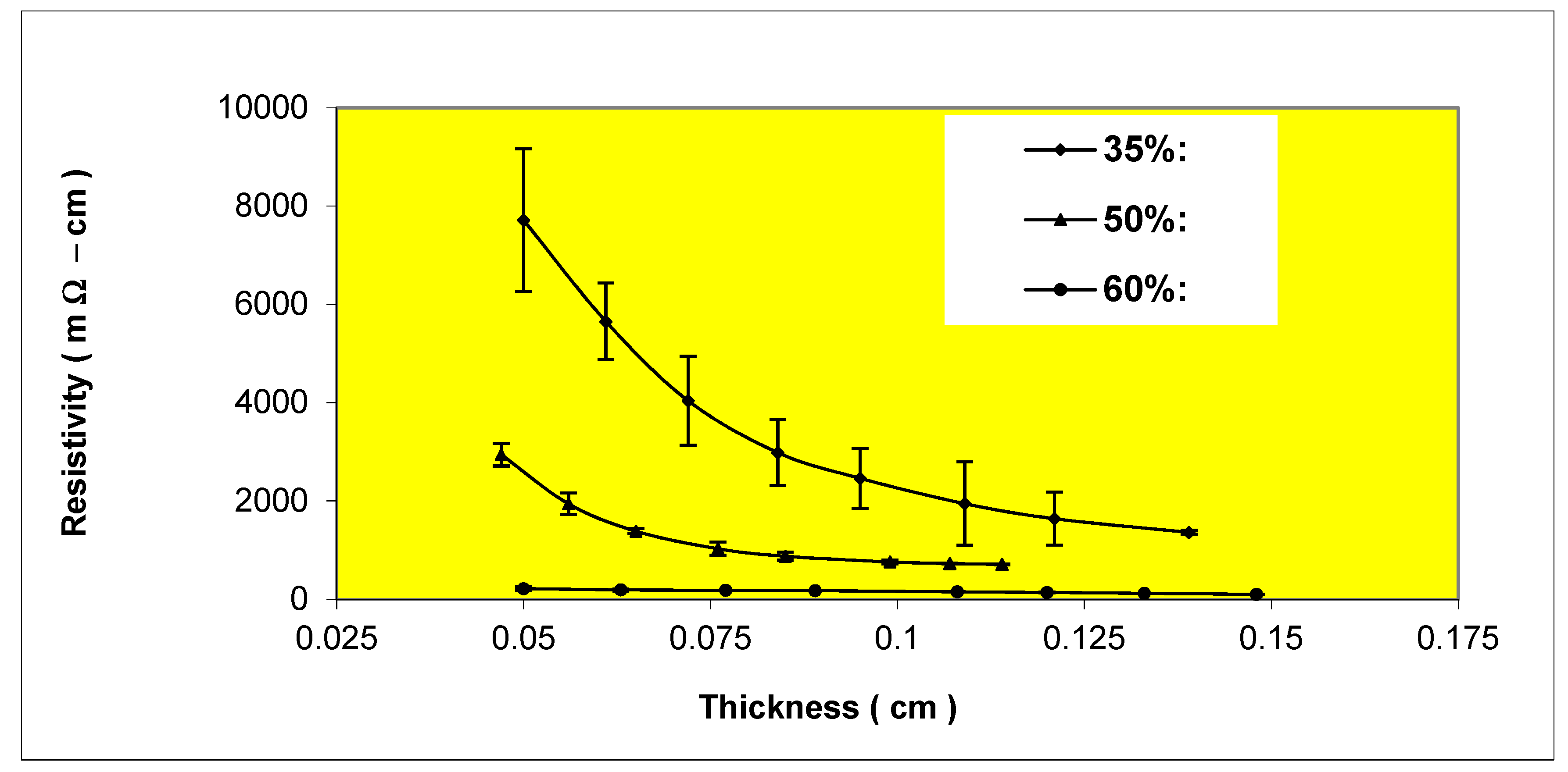
Variation of resistivity with thickness for Epon 830 films filled 35%, 50%, 60% by volume with (4-7 μm) silver powder.
Figure 7.
Variation of resistivity with thickness for Epon 830 films filled 35%, 50%, 60% by volume with (4-7 μm) silver powder.
Figure 8.
Variation of resistivity with thickness for Epon 830 films filled 40%, 50%, 60% by volume with etched (6-7 μm) copper powder.
Figure 8.
Variation of resistivity with thickness for Epon 830 films filled 40%, 50%, 60% by volume with etched (6-7 μm) copper powder.
Figure 9.
Variation of resistivity with thickness for Epon 830 films filled 35%, 50%, 60% by volume with etched (3-7 μm) nickel powder.
Figure 9.
Variation of resistivity with thickness for Epon 830 films filled 35%, 50%, 60% by volume with etched (3-7 μm) nickel powder.
Figure 10.
Variation of resistivity with thickness for Epon 830 films filled 35%, 42%, 50% by volume with etched (1-5 μm ) nickel flakes.
Figure 10.
Variation of resistivity with thickness for Epon 830 films filled 35%, 42%, 50% by volume with etched (1-5 μm ) nickel flakes.
Figure 11.
Variation of resistivity with thickness for Epon 830 films filled 35%, 50%, 60% by volume with etched (20 μm diameter) nickel filaments (260 µm).
Figure 11.
Variation of resistivity with thickness for Epon 830 films filled 35%, 50%, 60% by volume with etched (20 μm diameter) nickel filaments (260 µm).
Figure 12.
Modeling of hole depth effect on bonded sample resistance at hole diameter 2.74 mm for 60 % wt Ni (HCl-etched 3µm flake) / Epon 830 adhesive filled in Garolite sheets (McMaster-Carr, Aurora, OH) covered with 1.98 mm thick Al sheets.
Figure 12.
Modeling of hole depth effect on bonded sample resistance at hole diameter 2.74 mm for 60 % wt Ni (HCl-etched 3µm flake) / Epon 830 adhesive filled in Garolite sheets (McMaster-Carr, Aurora, OH) covered with 1.98 mm thick Al sheets.
Figure 13.
Microstructure of magnetically distributed 10% vol Ni filaments (20 µm diameter, 160 µm length) in ~ 0.02 cm thick Epon 815 epoxy film of ~ 25 mm² planar area, through which the magnetic field was applied (5000 Oe for 2 min).
Figure 13.
Microstructure of magnetically distributed 10% vol Ni filaments (20 µm diameter, 160 µm length) in ~ 0.02 cm thick Epon 815 epoxy film of ~ 25 mm² planar area, through which the magnetic field was applied (5000 Oe for 2 min).
Table 1.
Thickness-dependent resistivity of Epon 830 films filled with various particles.
Table 1.
Thickness-dependent resistivity of Epon 830 films filled with various particles.
Material
(50/50 by wt.
Proportions) |
Ag
(4-7 µm)
Powder |
Ag (4-7 µm)-
Ni (3- 7 µm)
Powder |
Ag-Ni (20 µm D*.
160 µm L*)
Filament |
Ag-Ni
(1-5 µm)
flake |
Ag-Ag Coated Ni (20µm) Flake |
| 3-D to 2-D |
None |
0.076 |
0.089 |
0.096 |
0.075 |
| transition thickness (cm) |
|
|
|
|
|
| |
|
|
|
|
|
| Highest resistivity |
0.093 |
7.34 |
13.6 |
740 |
37.2 |
| (mQ cm) at |
(0.058) |
(0.053) |
(0.051) |
(0.051) |
(0.045) |
| (cm thickness) |
|
|
|
|
|
| Average |
0.0728 |
3.05 |
4.57 |
81.5 |
8.14 |
| 3-D resistivity |
|
|
|
|
|
| (before 2-D transition) (mΩcm) |
|
|
|
|
|
| |
|
|
|
|
|
| Resistivity increase |
0.52 |
157 |
251 |
1491 |
970 |
| after 2-D transition |
|
|
|
|
|
| (per cm)* |
|
|
|
|
|
Table 2.
Volume resistivity of epoxy ECA’s filled with different types of conductive nanofibers.
Table 2.
Volume resistivity of epoxy ECA’s filled with different types of conductive nanofibers.
| Sample |
phr |
Volume Resistivity (ohm-cm) |
| Short Ni nanofiber filled-epoxy resin |
10 |
607 |
| Ag coated short Ni nanofiber filled-epoxy resin |
10 |
173 |
| Ni nanofiber mat filled-epoxy resin |
40.3 |
0.0145 |
Table 3.
Percent reduction in ultimate displacement and failure load values when the test machine crosshead rate is increased from 1 to 100 mm/min for specimens containing 35 and 60 % by volume Ni 110 particles.
Table 3.
Percent reduction in ultimate displacement and failure load values when the test machine crosshead rate is increased from 1 to 100 mm/min for specimens containing 35 and 60 % by volume Ni 110 particles.
| Substrate Surface/ Particle Volume Fraction Conditions |
% Reduction in Ultimate Displacement |
% Reduction in Failure Load |
| UE / Ni 110 35% |
42% |
25% |
| UE/ Ni 110 60% |
60% |
46% |
| E / Ni 110 60% |
69% |
42% |
Table 4.
Percent reduction in ultimate displacement and failure load values when the test machine crosshead rate is increased from 1 to 100 mm/min for specimens containing Ni 110 particles etched for 3 minutes (designated UE/PEI) or 5 minutes (designated UE/PEII).
Table 4.
Percent reduction in ultimate displacement and failure load values when the test machine crosshead rate is increased from 1 to 100 mm/min for specimens containing Ni 110 particles etched for 3 minutes (designated UE/PEI) or 5 minutes (designated UE/PEII).
| Particle Etching Condition |
% Reduction in Ultimate Displacement |
% Reduction in Failure Load |
| UE/ Etching I (UE/PEI) |
46% |
18% |
| UE/ Etching II (UE/PEII) |
39% |
15% |
| UE/ Unetched Particles |
50% |
30% |
