1. Introduction
Since its experimental demonstration, graphene has garnered global attention from researchers due to its mechanical, structural, thermal, and electrical properties, which make it highly attractive for engineering applications. The inherent properties of graphene have been explored in various fields, including flexible transparent circuits, electronic and optoelectronic device construction, chemical sensors, and energy storage [
1,
2,
3].
Over the past two decades, numerous carbon-based materials have been referred to as graphene, expanding upon its initial definition as "a monolayer of sp2-carbon atoms" [
1]. According to Zhu [
2], graphene has now become a generic term encompassing a wide range of carbon-based few-layer materials with distinct structures, morphologies, and sometimes even chemical compositions, heavily influenced by the preparation method.
There are two primary methods for manufacturing graphene: a top-down approach and a bottom-up approach, each with its own limitations and advantages. Antonova et al. [
1] discuss the bottom-up approach, which involves growing high-quality two-dimensional carbon layers through chemical vapor deposition or epitaxial growth on SiC substrates. This method allows for precise control over thickness by utilizing various substrate catalysts and growth parameters [
4].
In plasma applications, small graphene flakes with few layers can be produced without the use of substrates, employing a fast and controlled synthesis process. Plasma synthesis involves the decomposition of a carbon source, with carbon particle fragments formed within the gas phase of the plasma stream [
3,
5].
The deposition of graphene onto fiberglass has emerged as a promising area of research, leveraging the unique properties offered by both materials. Graphene, a two-dimensional carbon structure arranged in a hexagonal pattern, exhibits high electrical conductivity, exceptional mechanical strength, and a large surface area, making it an exceptional material for diverse technological applications [
6]. Conversely, synthetic fiberglass is known for its mechanical strength, lightweight nature, and durability, making it extensively utilized in sectors such as construction, automotive, and aerospace industries [
7].
Combining graphene with fiberglass could significantly enhance the mechanical properties of the resulting composite. Graphene possesses exceptionally high tensile strength, augmenting the strength and stiffness of fiberglass, rendering it more suitable for lightweight yet robust material applications [
7]. Additionally, the incorporation of graphene could improve the fatigue resistance of fiberglass, extending its lifespan under repetitive stress conditions.
Another advantage of depositing graphene onto fiberglass lies in its electrical properties. Graphene serves as an excellent conductor of electricity, facilitating the development of conductive composites when combined with fiberglass, which is an electrical insulator. This combination holds particular interest in applications within the realm of flexible electronics and sensory devices, where fiberglass with graphene can play pivotal roles in the transmission of electrical signals. This work presents a novel, simple, cost-effective, rapid, and scalable method of depositing graphene onto fiberglass using a non-thermal plasma system.
2. Experimental
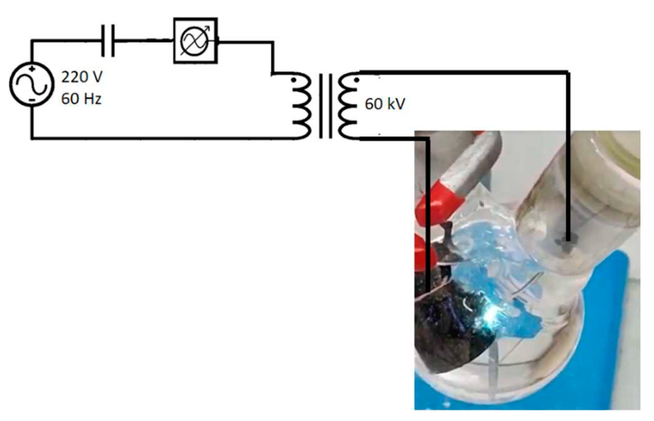
The graphene deposition on glass fiber was performed using a non-thermal plasma generator coupled to a reaction vessel, where an arc is created (
Figure 1). In this reactor, using cyclohexane (Aldrich) as input starting material, the 60 kV arc is applied with a flow of N
2(g) between a 316L steel electrode and another one made of mineral graphite, until there is no more liquid. The produced material is then collected in dimethyl-methanamide (Aldrich), sonicated for 15 minutes, and left to rest for 48 hours. Then, the supernatant is dried for 30 minutes in an oven at 180 °C. The same experimental procedure was used for depositing graphene onto glass fibers (Casa da Resina).
The dry material is characterized by transmission electron microscopy (TEM) using a JEOL JEM-2100 electron microscope, operated at 200 kV. The material obtained was characterized using scanning electron microscopy (SEM) Jeol JSM-6701F. The X-ray diffraction (XRD) were obtained using a diffractometer model Miniflex II, with Cu kα radiation source of 0.15406 Å, set at 2θ range 2–90°, with 2 min-1 scan speed. The Raman spectra were collected using a Horiba Scientific MacroRam Raman spectroscopy equipment with laser 785 nm. The Atomic Force Microscopy was used to observe the graphene deposit on the glass fibers and was carried out in a Multimode 8 using Peak Force Tapping mode and ScanAsyst-Air probe (resonant frequency ~ 70 kHz, spring constant ~ 0.4 N/m), both from Bruker, under ambient conditions.
3. Results and Discussion
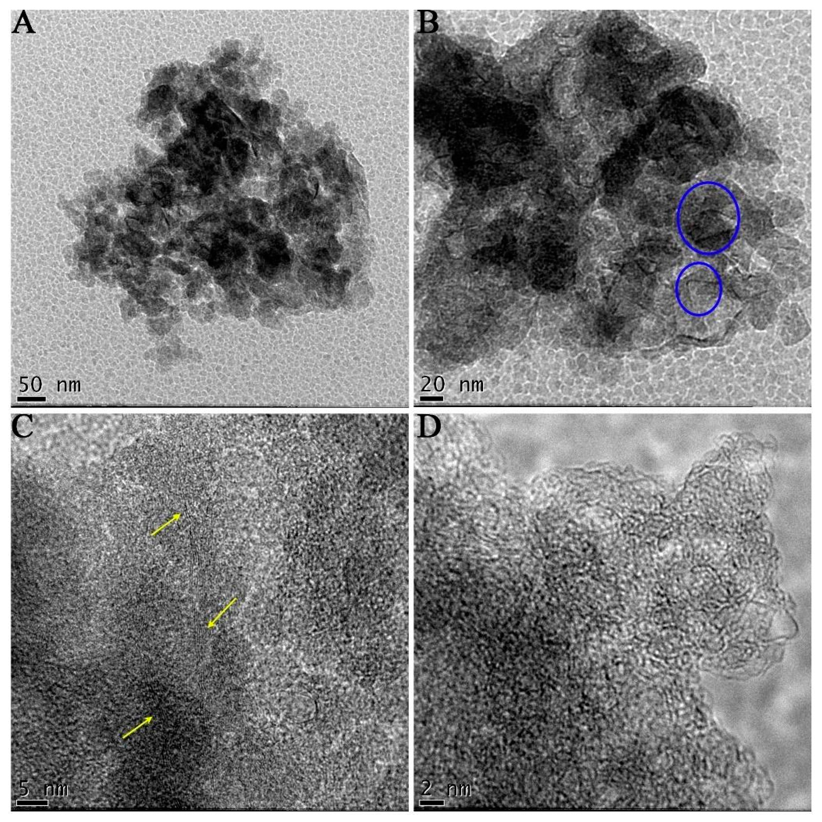
Figure 2 presents TEM images of graphene unsupported nanoflakes (GUN) obtained through non-thermal plasma with cyclohexane. In
Figure 2a, agglomerates of particles can be observed, with the transparent regions indicating ultra-thin nanoflakes measuring a few nanometers in size. Furthermore, slightly wrinkled regions are evident, contributing to the distinctive characteristics of graphene [
8,
9]. Moreover, the morphology of these nanoflakes, which are partially flat, along with regions exhibiting a low level of contrast, suggests a thin graphene layer thickness. However, the occurrence of disordered graphene flakes is also observed.
Figure 2b shows regions where the graphene nanoflakes were folded and, in some instances, curled edges were also observed. The layered structure of these nanoflakes is shown in
Figure 2c, where there are stacks of about 5 or more layers. Due to the high resolution of the TEM (
Figure 2d), it is possible to state that the graphene nanostructure is not perfectly flat. It has a partially wrinkled surface that can be designated by regions with different levels of transparency, as discussed above. These nanostructural features provide graphene flakes with promising electronic properties [
9].
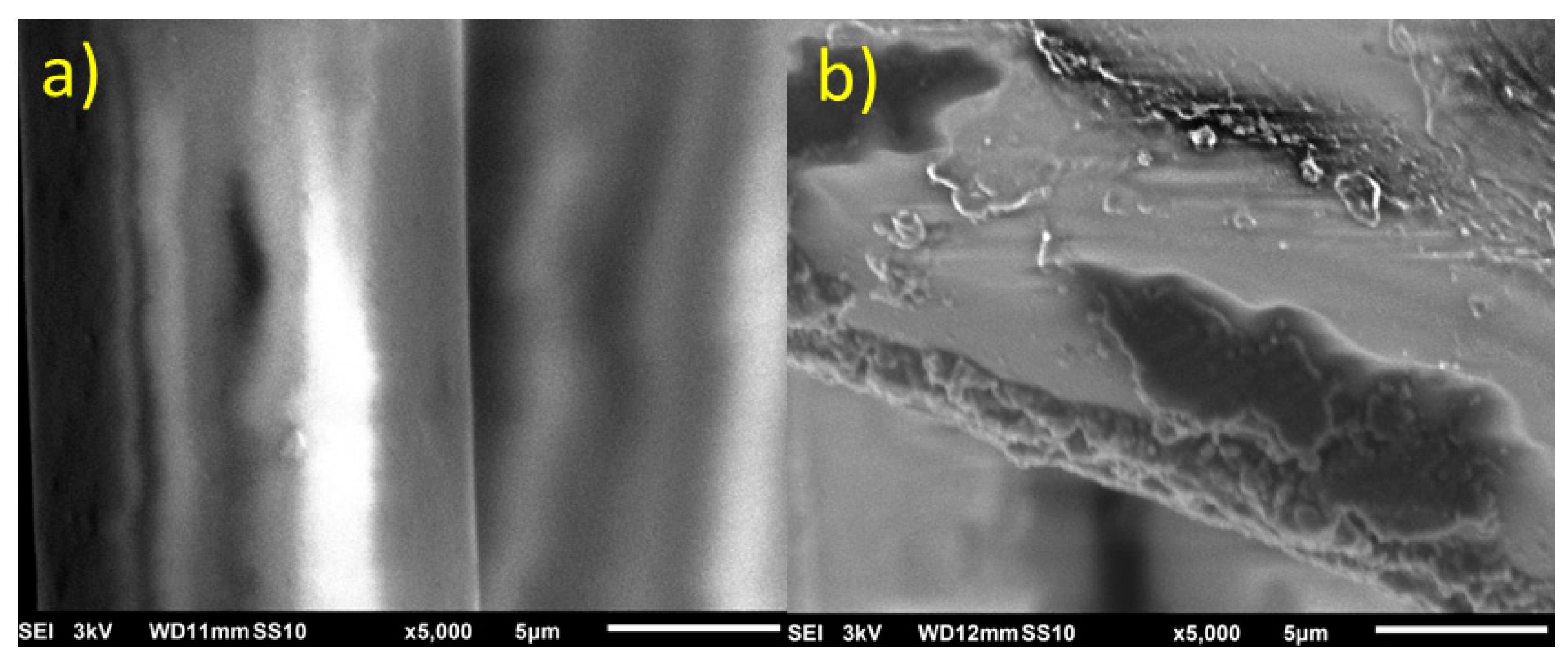
SEM images (
Figure 3) reveal the smooth and shiny appearance of the fiberglass, similar to what has been reported by other authors in the literature [
10,
11]. However, after subjecting the fiberglass to the graphene deposition process using non-thermal plasma, referred in text as a Graphene Nanoflake/Fiberglass (GN/Fiberglass), clear encrustations of carbonaceous material can be observed on the previously smooth surface. Additionally, surface roughness and defects are noticeable, likely caused by the exfoliation process facilitated by this synthesis setup [
12].
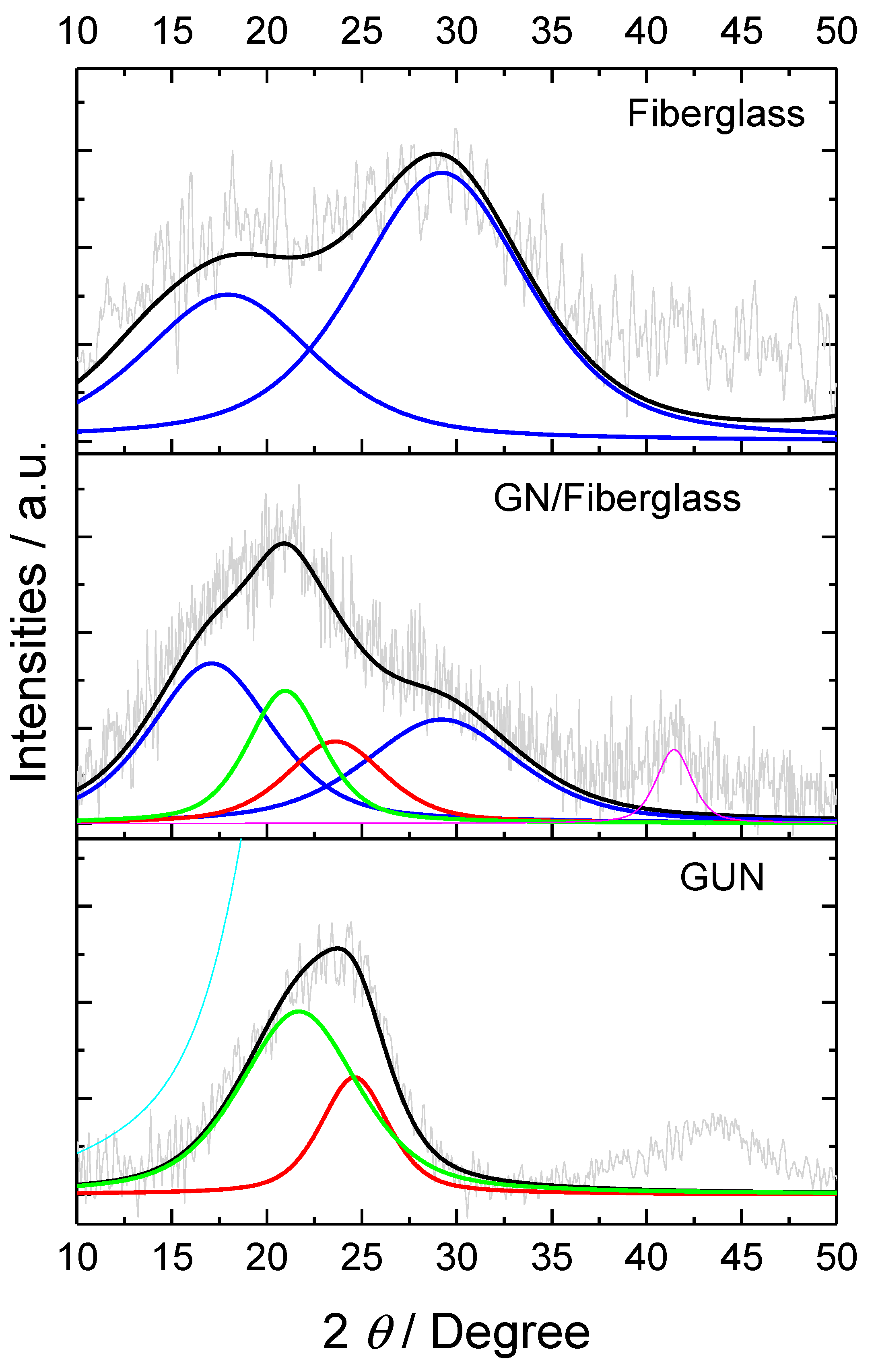
Figure 4 presents the X-ray diffraction (XRD) analysis of the fiberglass, revealing peaks at 2θ = 18.8 and 28.9° corresponding to silicon oxides (JCPDF 38-360). For the GUN, the diffraction pattern provides evidence of nanoflake stacking and crystallite size within the graphene plane. This evidence can be observed from the (002) and (100) planes, which further corroborates the data obtained from TEM analysis. The presence of a broad peak at 2θ = 24.62° may suggest a structure with a lower degree of crystallinity. Moreover, the data indicate a degree of amorphism of approximately 48%, where the partially disordered structure exhibits a d-spacing of approximately 0.358 nm between graphene layers. Additionally, the presence of defects affirms the existence of regions in the graphene sheets with increased folding and edge areas, as observed in the TEM images. The peak corresponding to crystallographic plane (100) presents a d-spacing of 0.208 nm for graphene; this observation suggests the formation of few-layer graphene (FLG) [
13]. In the material with Graphene Nanoflakes on Fiberglass surface (GN/Fiberglass), it was noted that the peaks related to carbon phases are shifted by approximately 1° towards a less positive 2θ angle, with a d-spacing of 0.2134 for the (100) plane. This indicates an increase in the spacing between graphene layers. Furthermore, there is a degree of amorphism of approximately 55%, where the partially disordered structure exhibits a d-spacing of approximately 0.364 nm between graphene layers.
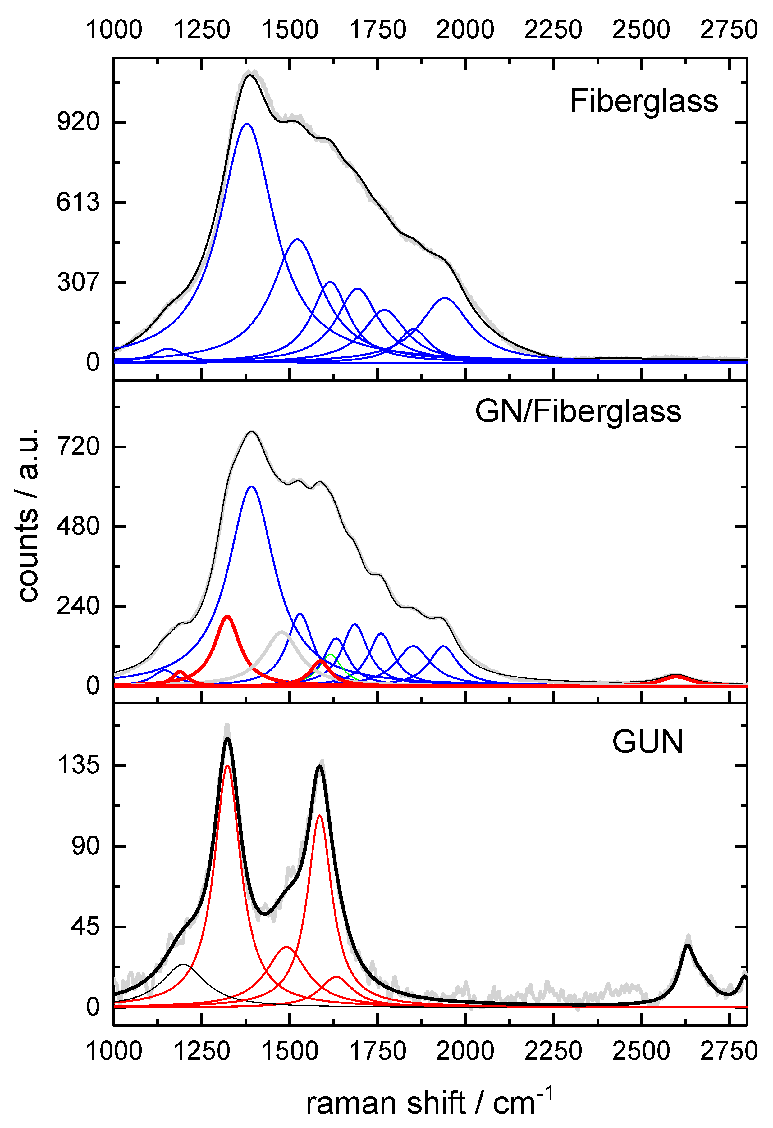
The Raman spectroscopy analysis provides us with related information, such as the quality of graphene, based on the detailed position, width, shape, and relative amplitude of the peaks. It can also corroborate the TEM and XRD analyses discussed so far. In the Raman spectrum of fiberglass (
Figure 5), one can observe the bands at 1149, 1625, and 1691 cm
-1, which are related to silicon bonded to aluminum, oxygen, and hydrogen [
14,
15,
16]. Additionally, the bands at 1385, 1527, 1763, 1847, and 1930 cm
-1 correspond to boron bonded to hydrogen, boron, and oxygen [
17,
18,
19,
20]. In the spectrum obtained from GUN, it is possible to observe the three characteristic peaks of graphene: the D, G, and 2D bands centered at approximately 1320, 1585, and 2640 cm
-1, respectively [
21]. The observed peaks in the D and G bands are the result of the convolution of the D1, D2, D3, D4, and G modes in the lower frequency regions of the spectrum at approximately 1322, 1623, 1495, 1196, and 1587 cm
-1 [
22].
For the GN/Fiberglass material where the convoluted bands of fiberglass interfere with the resolution of the D and G bands of graphene due to the small amount of material deposited on the fiber, the D2 band of graphene is suppressed. This suppression is likely due to the low intensity nature of the D2 band which occurs when a small quantity of material dopes the fiberglass; this is also an indication that the nanoflake was incorporated into the fiberglass.
The literature extensively discusses that the G-band corresponds to first-order scattering of
E2g mode which is related to
sp2 carbon. Additionally, the D band can be attributed to structural defects carbon amorphism or edge defects that can affect symmetry and selection rules [
23]. The G band is characterized by number of layers as it reflects contribution of vibration modes from more carbon atoms. Its intensity shape and position provide indications of induced deformations. In literature Raman intensity ratio of D-band to G-band (
ID/
IG) is a critical parameter for characterizing degree of disorder in graphene [
21]. In both cases characteristics of graphene nanoflakes were observed with ratio of 1.36 for GUN and approximately 3 for GN/Fiberglass indicating increase in defects and doping of carbon structure by components of fiberglass. This is entirely possible considering energy employed in synthesis method which is capable of exfoliating crystalline structures such as NB [
12].
However 2D frank band positioned at 2631.4 cm
-1 may indicate presence of randomly arranged and disordered graphene sheets as discussed earlier in TEM analyses [
13]. Literature indicates that defects observed in graphene nanostructure may be caused by high anisotropy of mechanical strength or electrical conductivity between in-plane and out-of-plane directions which can improve material performance for electronics and catalysis applications [
24].
Furthermore 2D peak may indicate folded graphene structure as observed in TEM and XRD data. This effect may be result of accumulation of amorphous carbon during material formation [
25]. The Non-hexagonal defects observed in discussed graphene nanostructure can increase the reactivity of the basic planes, making these materials active and efficient in heterogeneous catalysis [
24].
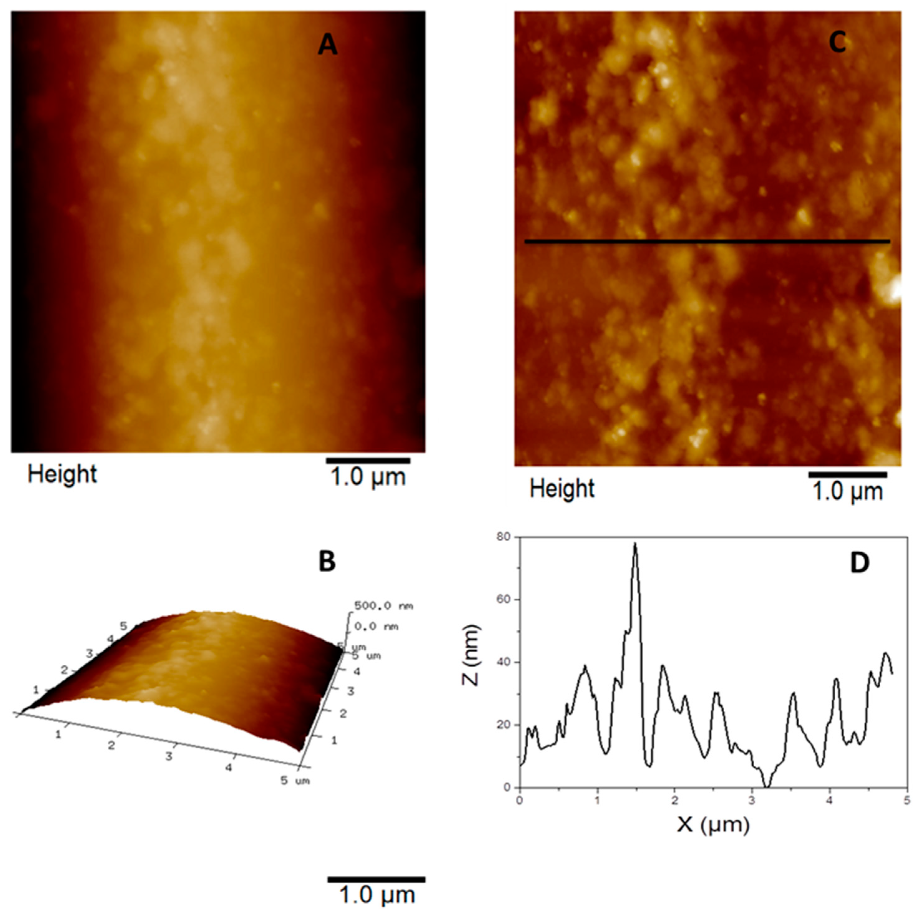
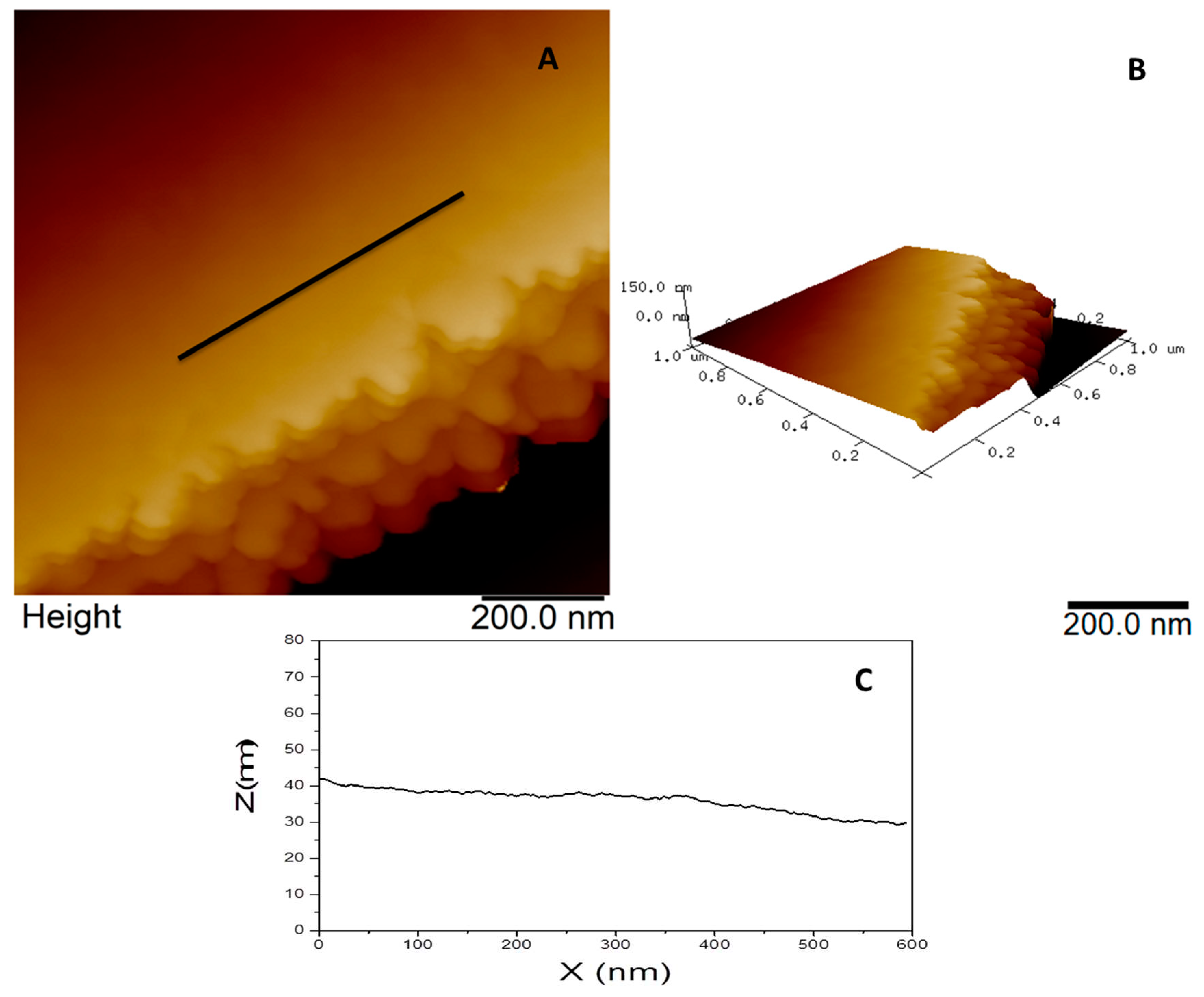
Figure 6 and
Figure 7 illustrate the fiberglass and the graphene nanoflakes deposited on fiberglass performed by AFM to support the understanding of the fiberglass surface and the formation of graphene layers on it at the nanometric scale. The fiberglass clean has a slight curvature and an irregular surface, as shown in
Figure 6a,b, which couldn't be seen by SEM analysis (
Figure 3a). For a more detailed visualization of the surface irregularities present on it, image 6a was flattened prior to the section analysis (
Figure 6c) and the corresponding profile can be observed (
Figure 6d) with peaks around 30 nm and regions reaching 70 nm in height.
Figure 7a presents topographic AFM image of graphene deposition on a fiberglass, where is possible to see a regular and smooth surface, the layer border shape and how they are stacked in multilayers (
Figure 7a,b). The line profile from
Figure 7a is represented in
Figure 7c and it is in the same “Z” scale from
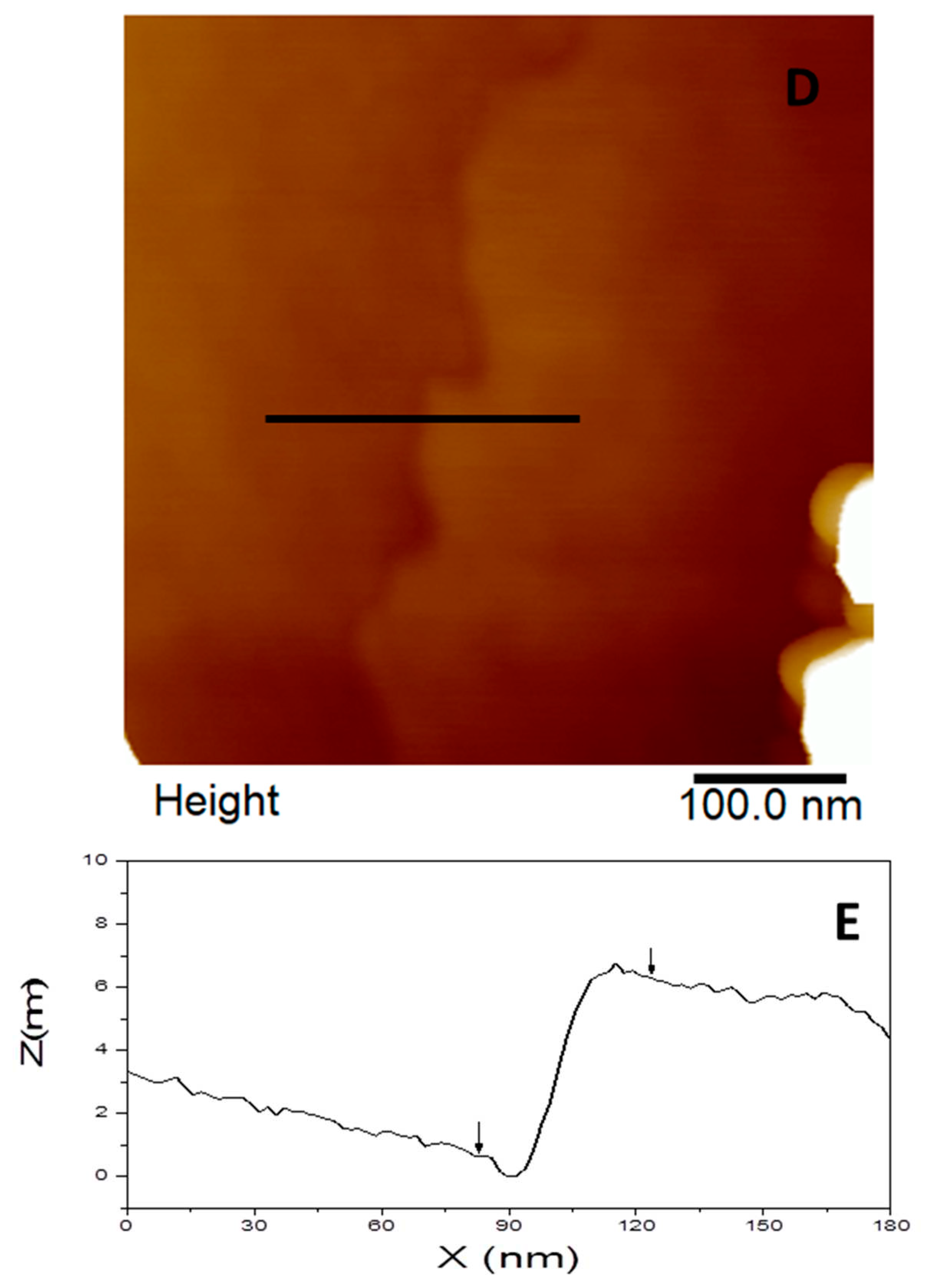
Figure 6c to better visualization and comparison. In a smaller scan size (
Figure 7d), a step can be seen in detail and a vertical distance around 5.7 nm was measured (
Figure 7e).
