1. Introduction
Infrared sensors which consist of a pyroelectric thin film sandwiched between two metallic electrodes produce an electrical voltage (or current) in response to temperature variations. In recents decades, they are widely used in fire detection, intruder alarms, infrared light detection and imaging, body temperature monitoring, and so on [
1,
2,
3,
4,
5]. Moreover, pyroelectric sensors can be easily integrated with modern IC circuits to realize sophisticated system-on-chip (SoC) devices for a wide variety of sensing and detection applications [
6,
7].
Lienhard and Heepmann [
8] investigated the transmittance of thin nickel (Ni) films deposited on pyroelectric polyvinylidene fluoride (PVDF) films over the infrared spectral range of 2–50 μm. It was shown that an appropriate specification of the Ni film thickness could effectively control the absorbance characteristics of the pyroelectric sensor. Hashimoto et al. [
9] developed a pyroelectric detector incorporated a thin PbTiO
3 ceramic film with a thickness of approximately 40 μm and a supply voltage of 5 V to construct a people-counting system for detecting the moving direction and number of passersby at a door. The detector showed a maximum sensitivityof voltage response of 23 mV/mW at a chopping frequency of 10 Hz. Chang and Tang [
10] fabricated an integrated pyroelectric sensor consisting of a PZT thin film and a Si JFET. The device implemented with a 500 μm thick silicon substrate was characterized over a modulation frequency range of 0.2 to 10 Hz and had a voltage sensitivity of 191 mV/mW at a modulation frequency of 1 Hz. Recently, Pb(Zr, Ti)O
3, (Bi, Na)TiO
3, (Sr, Ba)NbO
3, Pb(Sc, Ta)O
3, (Ba, Sr)TiO
3 and Pb(Zr, Sn, Ti)O
3 were investigated to be suitable for pyroelectric detection applications [
11]. Chong et al. [
12] fabricated a thin-film pyroelectric sensor array consisting of 16 sensing elements made of metal–ZnO–metal sandwiched layers with dimensions of 200 μm × 200 μm. The sensor response was enhanced to be a maximum voltage sensitivity of 110 mV/mW by depositing the sensing elements on a thermally isolated and freestanding Si
3N
4/SiO
2 membrane at a cutoff frequency of 20 Hz. The membrane was created by removing the underside of the SiO
2 substrate using a conventional back-etching technique.
Hsiao et al. [
13] fabricated a ZnO pyroelectric sensor on a back-etched silicon wafer using a two-step radio frequency (RF) sputtering technique. A ZnO film with preferred
c-axis orientation and an enhanced voltage response could be found by the use of the two-step deposition process. The sensor achieved a maximum voltage sensitivity of 8.6 mV/mW at a cutoff frequency of 500 Hz when implemented with a Ni coating on the uncovered part of the ZnO film in order to enhance the absorption of the incident energy. Hsiao et al. [
14] developed a pyroelectric sensor consisting of a zinc oxide (ZnO) sensing layer, gold (Au) upper and lower electrodes, and a supporting silicon (Si) substrate. The response voltage of the device was measured for three different line widths of the upper electrode given different values of the thin film thickness. The results showed that the optimal electrode width decreased as the thickness of the ZnO sensing film reduced. The maximum voltage response was obtained for a line width of 30 μm and ZnO thickness of 1µm. Wei et al. [
15] fabricated ZnO pyroelectric sensors with partially covered and fully covered electrodes, respectively, for performance comparison. The experimental results showed that the responsivity of the partially covered device was around four times higher than that of the fully covered device for incident light frequencies in the range of 10–1000 Hz. Liu et al. [
16] deposited a thin Ni layer on the surface of a PZT pyroelectric sensor as both the top electrode and a selective absorption layer. The maximum absorption coefficient of the resulting sensor was found to be 0.8 at a wavelength of 0.664 μm and 0.7 at a wavelength of 4 μm. Gaur et al. [
17] developed a miniaturized pyroelectric infrared sensor consisting of two polycrystalline aluminum nitride (AlN) films deposited on either size of a Si wafer, a silicon dioxide (SiO
2) insulating layer, and thin chromium (Cr) and Au electrodes. The sensing performance of the proposed device was improved through the sputtering of an additional Au film on the Ag film to enhance the infra-red absorptivity and increase the temperature gradient between the sensing film and the substrate. It was shown that the device had a response time of 8.0 ms and a current responsivity of 2.5 × 10
-6 A/W. Lee [
18] fabricated a pyroelectric infrared sensor incorporating a ZnO sensing layer, a thermally-insulated Si substrate, and Au upper and lower electrodes. The backside of the wafer was selectively etched to create a suspended sensing structure. Moreover, the responsivity of the device was enhanced by annealing the thin film at 500℃ for four hours. The numerical and experimental results showed that the voltage responsivity of the proposed device improved as the substrate thickness reduced.
One of the most common applications of infrared sensors is that of position sensing. Kim [
19] proposed an indoor positioning system consisting of three infrared emitters (scanner) placed at known positions and a mobile incident angle sensor attached to a moving target to measure the angle differences between each pair of emitters. Gorostiza et al. [
20] proposed a method for achieving the accurate localization of mobile robots in intelligent spaces by sensing the infrared signals emitted by the robots and then applying a hyperbolic trilateration method to the corresponding differential distances. Luo et al. [
21] constructed a wireless sensor network consisting of pyroelectric infrared sensor arrays as nodes and processed the signals emitted by the sensors using a filtering algorithm to detect human motion and perform activity recognition. Yan et al. [
22] investigated the various macro and micro factors affecting the ability of pyroelectric sensor systems to perform human identification. The results showed that the recognition performance improved with a closer distance, a faster moving speed, and a greater number of signal modulation mask holes. Agmell et al. [
23] constructed an indoor localization system for AGVs based on mobile receivers and infrared scanners mounted on the wall. Zhang et al. [
24] proposed a low-cost and robust method combining infrared vision and ultra-wideband (UWB) fusion for the indoor localization of mobile robots. It was shown that a centimeter-level of positioning accuracy could be obtained by applying an adaptive weight positioning algorithm to detect the edge of the UWB coverage area and fusing the outputs of the two sensing mechanisms using an extended Kalman filter (EKF). Wu et al. [
25] presented pyroelectric detection and sensing signal processing algorithms to create a non-wearable cooperative indoor human localization system based on pyroelectric sensor networks.
The present study proposes an approach for performing target object localization in indoor environments using a trilateration approach based on three miniaturized ZnO-based pyroelectric infrared sensors. The voltage readings of the three sensors are interfaced to a computer through low-noise current preamplifiers, and the signals are then fused and processed using a self-written LabVIEW human-machine interface to determine the position of the target object in two-dimensional space.
2. Principles and Designs
The pyroelectric phenomenon is primarily generated by the influence of the environmental temperature on the charged substances within the crystal structure of the sensing material. Assume that infrared light with a power
W(t) sinusoidally modulated at a frequency
is incident on the surface of a pyroelectric sensing element with a pyroelectric coefficient
p, an electrode area
A, thickness
d and surrounding temperature
T. The incident power can be formulated mathematically as follows [
26]:
where
i =
ApdT/
dt.
Assume further that the sensing element has a thermal capacity
HT, and the thermal conductance to the surroundings is denoted as
GT, giving a thermal time constant of
. Given an emissivity
, the temperature difference between the element and its surroundings,
, can be described as [
26]:
which has the solution [
26]:
Differentiating Equation (3), the rate of the temperature difference between the element and its surrounding is obtained as:
In particular, a change in the temperature induces a stress variation within the sensing layer, which is manifested by a measurable change in the electrical charge and output current of the device. The pyroelectric variation rate,
, can be expressed as follows:
where
is the temperature change.
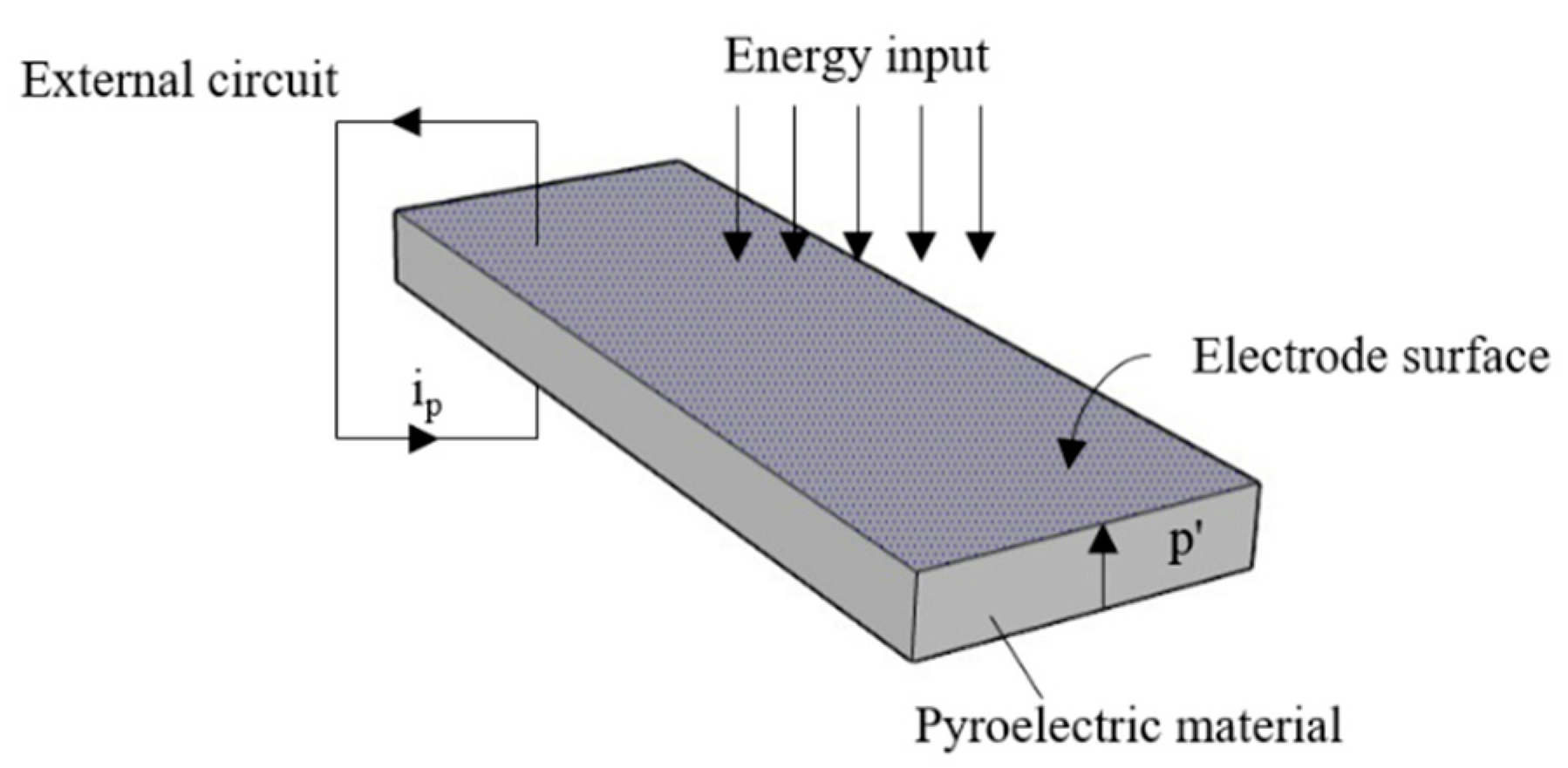
Figure 1 illustrates the basic operation of a pyroelectric sensor with a surface area A and pyroelectric coefficient component
p' in the vertical direction. When exposed to an input energy flux, the pyroelectric current which flows through the external circuit is given by
It can be found that the pyroelectric sensor is “AC coupled” to any input energy flux which generates a change in temperature, where this input may primarily take the form of electromagnetic radiation absorbed in the pyroelectric material.
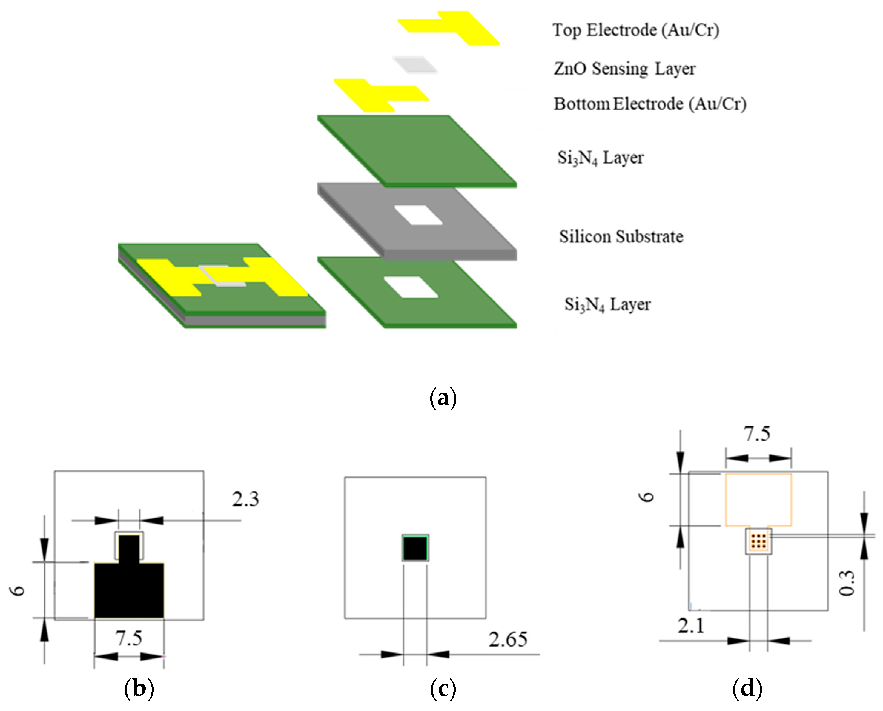
Figure 2(a) presents a structural assembly diagram of the thin-film pyroelectric infrared sensor proposed in the present study based on a single-side polished Si wafer substrate with a thickness of 525
+25 μm. As shown, the substrate is coated on both sides with a silicon nitride (Si
3N
4) insulating layer with a thickness of 1 μm. The bottom and top electrodes each comprise a layer of Cr with a thickness of 0.03 μm and a layer of Au with a thickness of 0.1 μm and have the configurations and dimensions shown in Figs. 2(b) and 2(c), respectively. Finally, the sensing layer has the form of a 0.89-μm thick ZnO film sandwiched between the top and bottom electrodes and having the dimensions shown in Fig. 2(d).
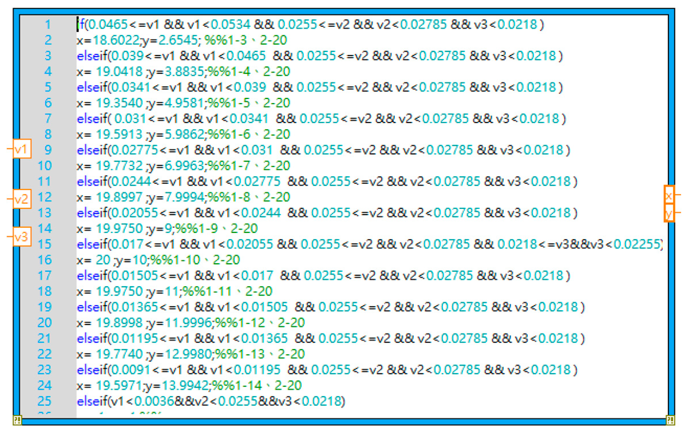
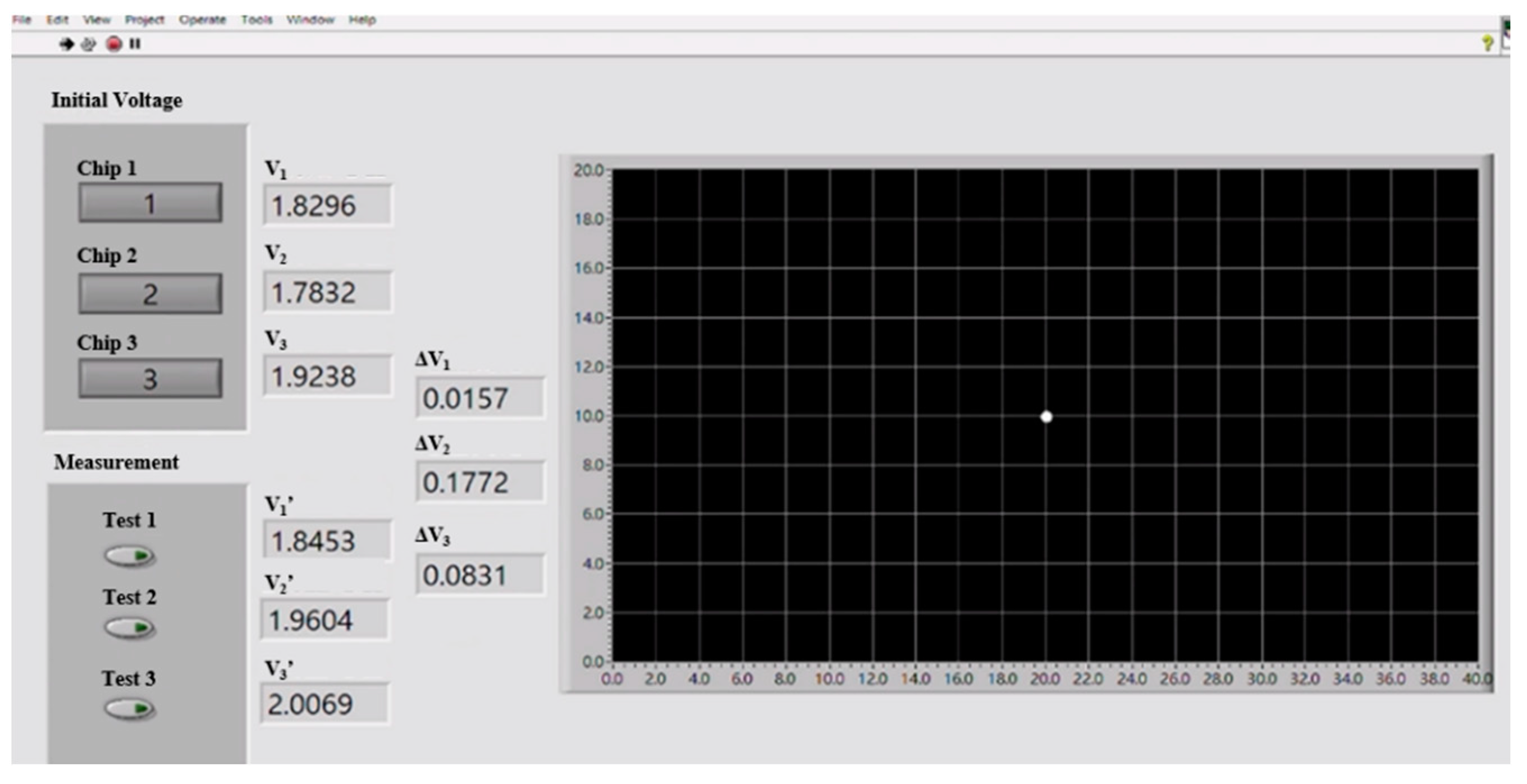
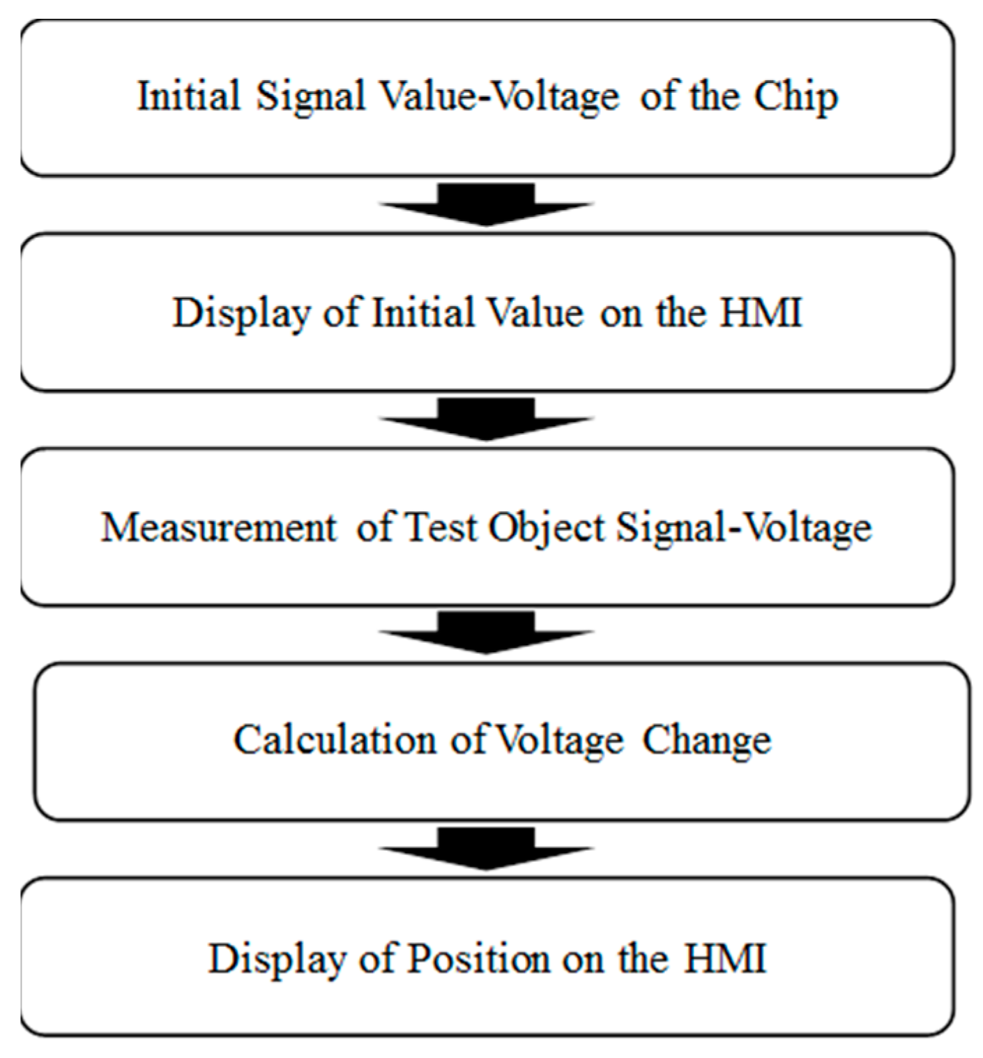
Figure 3 shows the basic steps in the self-written LabVIEW program used to perform target object detection in the present study. Upon receiving the initial voltage signal of the pyroelectric sensor in the absence of an infrared target object, the program measures the voltage and displays it on a human-machine interface (HMI). Following the introduction of the target object into the sensing field, the program measures the voltage once again, calculates the voltage change, and presents it on the interface. The voltage change is then input to the MathScript module in LabVIEW to determine the position of the object using a triangulation-based method. Finally, the computed coordinates of the target object in the two-dimensional (2D) sensing field are displayed on the HMI.
3. Methods and Fabrication
3.1. Fabrication
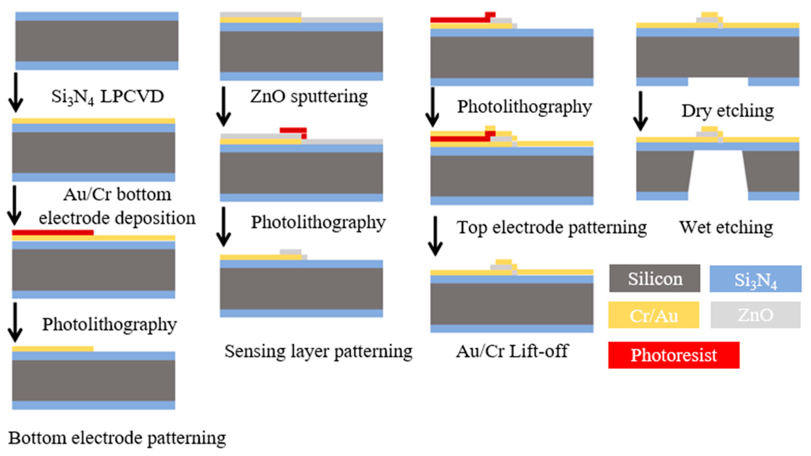
Figure 4 shows the main steps in the sensor fabrication process. The process commenced by patterning the bottom electrode. A low-pressure chemical vapor deposition (LPCVD) method was first employed to deposit a 1-μm thick Si
3N
4 film on both sides of a single-side polished P-type silicon wafer substrate as an insulating layer. The deposition process was performed using high-purity chemical gases with a chamber pressure of less than 10 Torr. A 300-Å thick Cr adhesive layer and 1000-Å thick Au conducting layer were then deposited on one side of the substrate using an electron beam evaporation technique to form the bottom electrode. The electrode was patterned using a standard photolithography method.
Having patterned the lower electrode, a ZnO sensing layer was deposited on the electrode using a high vacuum magnetron sputtering system using a 4N purity grade 4” ZnO target. The wafer was placed in the chamber, and the chamber was vacuumized down to 5×10⁻⁶ Torr. A pre-sputtering process was performed using argon (Ar) gas to remove any oxides or impurities from the target surface. In the pre-sputtering process, the target power was increased at a rate of 10 W per minute until it reached 150 W and the target was then bombarded by Ar ions for 30 minutes.
The upper electrode was patterned using photoresist, and a 300-Å thick Cr layer and 1000-Å thick Au layer were deposited using an electron beam evaporation method. The photoresist layer was removed using acetone solution to leave behind just the desired pattern of the top electrode.
In the final step of the fabrication process, a backside etching technique was used to release the sensing structure. A photolithography process was first performed to define the etching area on the backside of the wafer. Reactive ion etching (RIE) was used to remove the Si3N4 insulation layer from the wafer surface and wet etching was then performed in a 30 wt% potassium hydroxide (KOH) aqueous solution at a temperature of 80℃ for 6 hours to produce a final suspended film thickness of 1 μm.
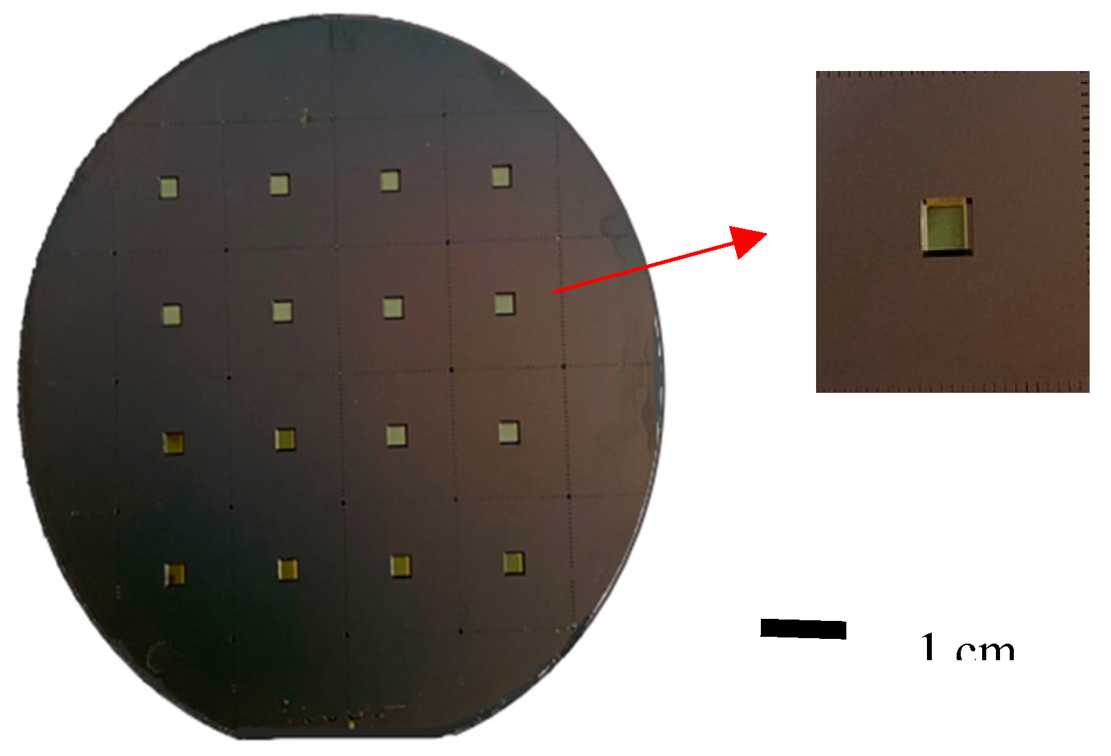
As shown in Fig. 5, sixteen infrared sensing chips were fabricated on a single silicon wafer. Four square alignment marks located at the four corners of the photomask were used to ensure a precise alignment of the mask during the patterning process.
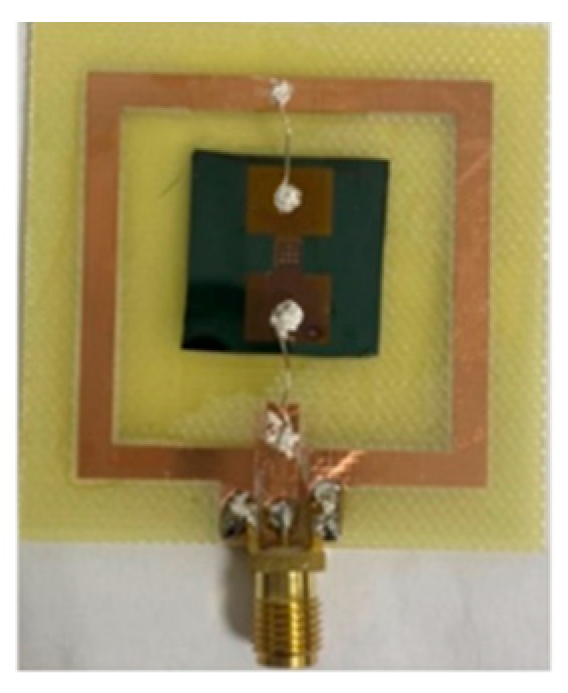
Figure 6 presents a photograph of the final sensor.
Figure 4.
Process flowchart showing main steps in sensor fabrication process.
Figure 4.
Process flowchart showing main steps in sensor fabrication process.
Figure 5.
Photographs of back-etched chip.
Figure 5.
Photographs of back-etched chip.
Figure 6.
Photograph of finished pyroelectric infrared sensor.
Figure 6.
Photograph of finished pyroelectric infrared sensor.
4. Results and Discussion
This section commences by analyzing the structure and surface morphology of the ZnO pyroelectric sensing layer. The voltage response of the device is then investigated as a function of the distance from the target object. Finally, the feasibility of the proposed sensor for target object detection and localization is demonstrated.
The ZnO film was sputtered using pure argon (Ar) as the working gas and was then annealed at 500℃ for 4 hours. The structure of the annealed ZnO film was examined by X-ray diffraction (XRD) using monochromatic Cu-Kα with a wavelength of λ=0.154 nm as the excitation source. Scanning was performed over a range of 2θ=30 ~ 60° with a sampling interval of 0.03° and a sampling time of 0.45 seconds. The analysis was conducted using an operating voltage of 40 kV and an operating current of 40 mA.
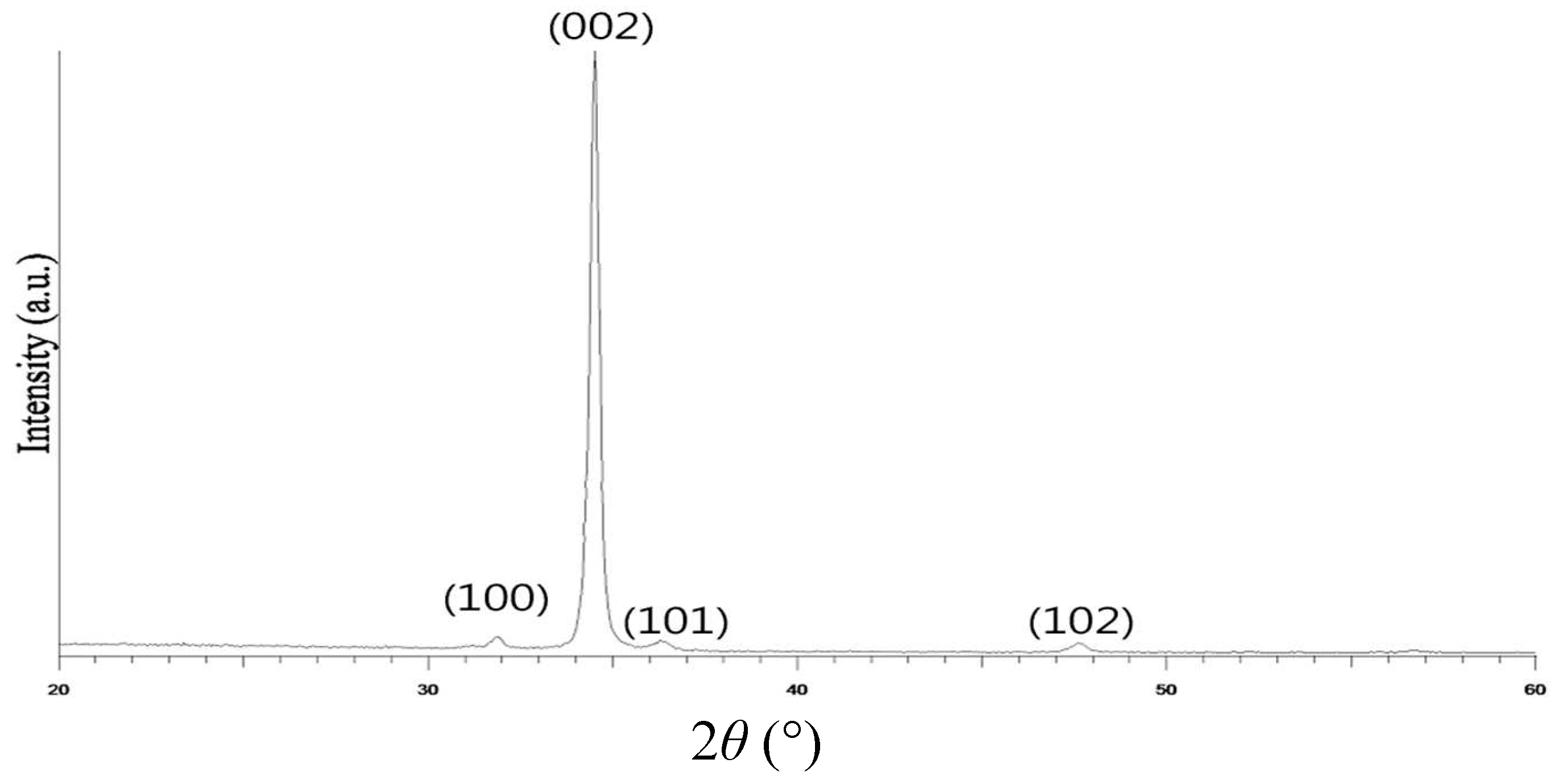
The XRD pattern for the annealed ZnO film is shown in Fig 7. The results indicate that the strongest peak is associated with the (002) crystal orientation. Thus, the ZnO film is inferred to have a wurtzite structure [
18].
Figure 7.
XRD pattern of ZnO sensing film.
Figure 7.
XRD pattern of ZnO sensing film.
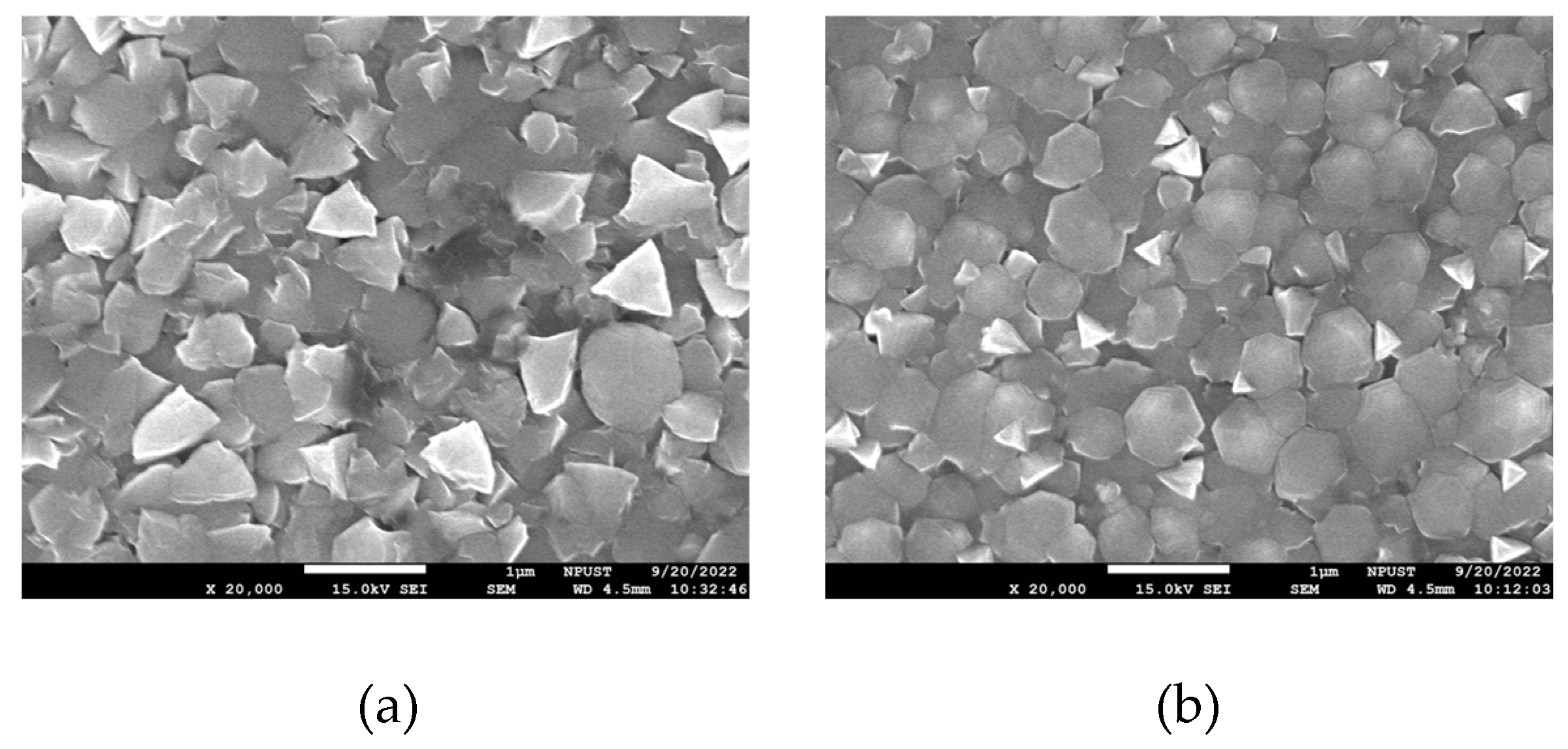
Figure 8(a) and (b) present SEM images of the surface morphologies of the as-deposited and annealed ZnO thin films, respectively. The as-deposited surface has a flake-like morphology with relatively large gaps and voids between the grains. Following the annealing process, the particle size increases while the voids and gaps decease in both size and number. Thus, the pyroelectric current signal transmission capability is improved, as discussed in [
18].
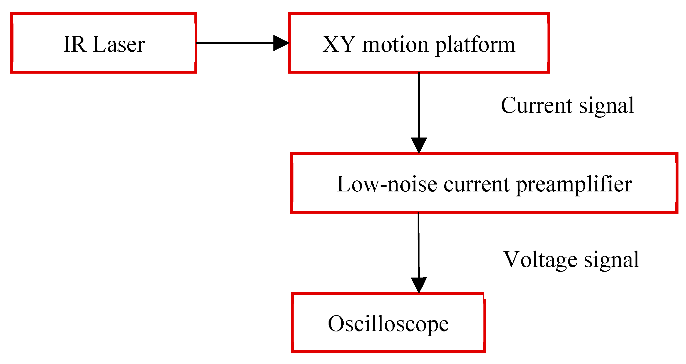
Figure 9 illustrates the basic structure of the measurement platform constructed in the present study. The sensor was placed on an X-Y platform and a human palm was utilized as the thermal source for infrared signals. The sensor signal was interfaced to an SR570 low-noise current preamplifier (Stanford Research Systems) via SMA connectors, and the resulting voltage signal was displayed in real time on an oscilloscope (TDS 2001C, Tektronix, USA).
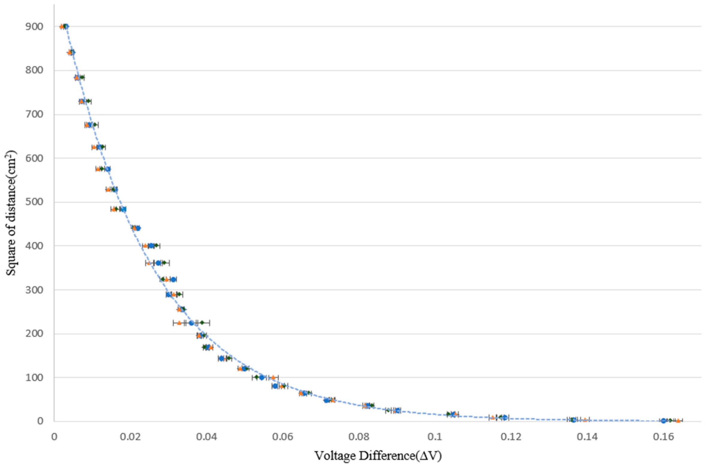
Figure 10 presents the experimental results obtained for the variation of the voltage change of the infrared sensor with the square of the distance between the sensor and the human palm. As expected, the voltage response increases as the sensing distance reduces. The voltage change is related to the square of the sensing distance inversely and exponentially with a correlation coefficient of R
2 = 0.9885. Moreover, the voltage response is particularly pronounced for sensing distances in the range of 0 ~ 30 cm.
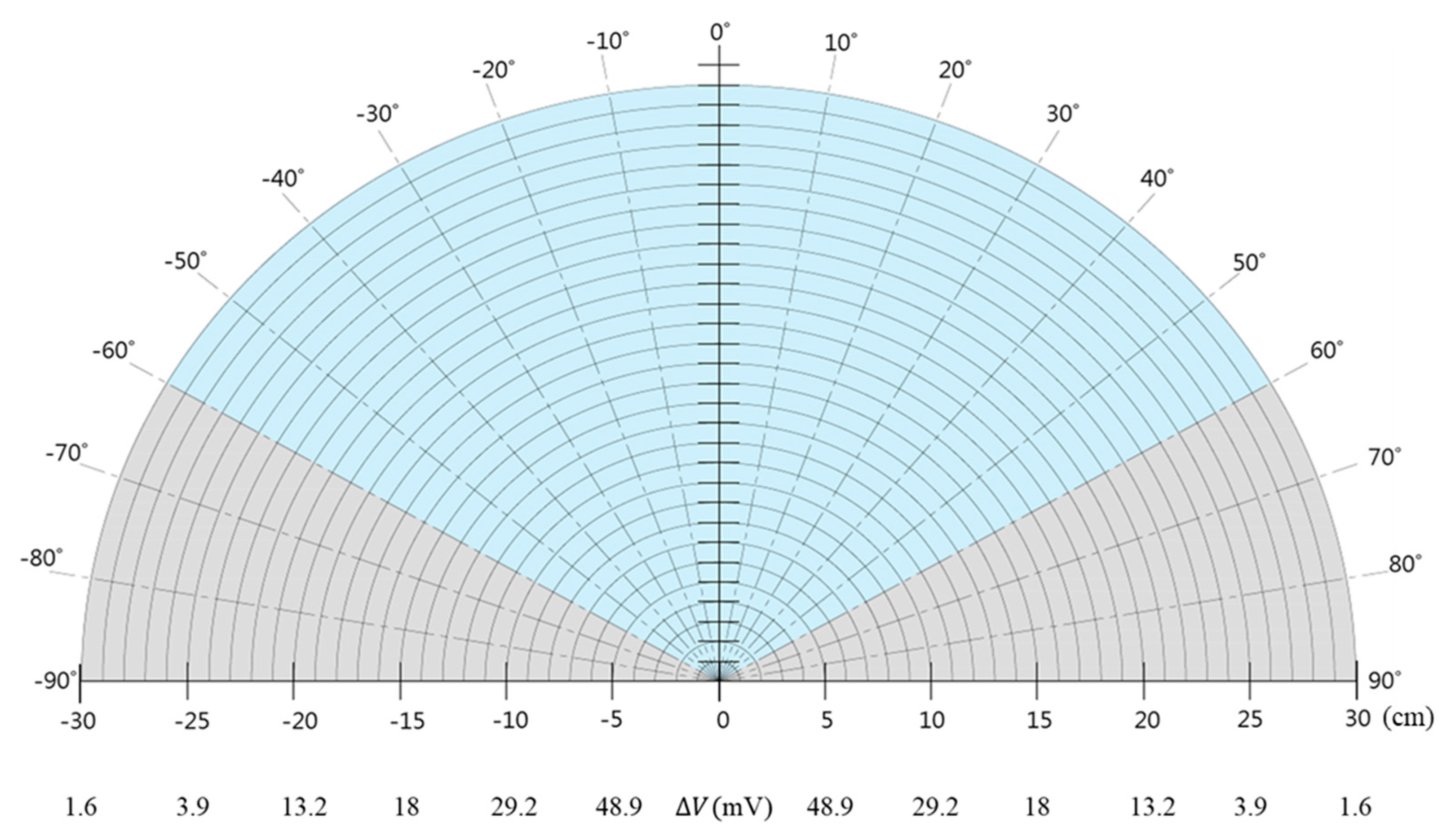
Figure 11 shows the measured voltage change of the sensor over a distance of 0 ~ 30 cm as the position of the human palm relative to the sensor was rotated through 180°. It is seen that the voltage variation is identical at equidistant points over the range of 120° in front of the sensor (as indicated by the blue region). Hence, in developing the target object positioning system proposed in this study, the sensing angle range of each sensor was set as 120°. Within this range, the voltage varied from 1.6 mV at a distance of 30 cm to 160 mV at a distance of 0.1 cm.
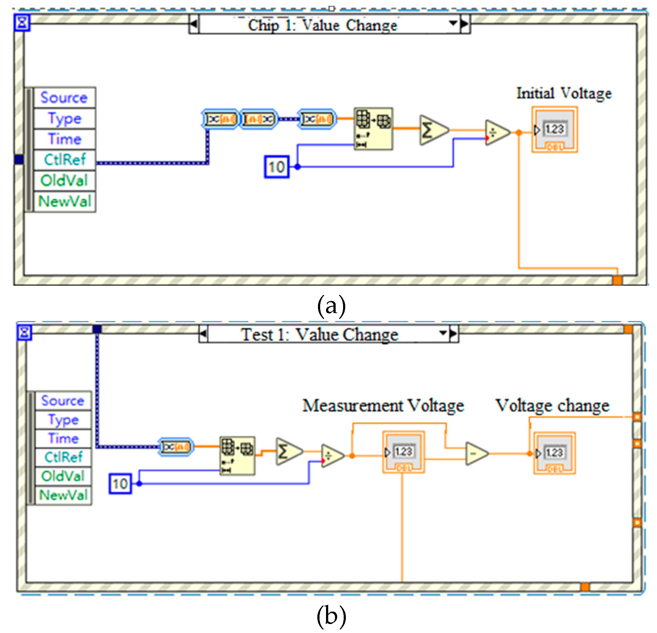
A target object detection system was constructed using a system of 3 sensors. For each sensor, the acquired data were converted into a 1D array of scalars, representing a single channel of voltage values. Due to slight fluctuations of the voltage signal, 10 data points were averaged to obtain a mean value when determining the initial voltage (no target object) and measurement voltage (with target object) of the sensor respectively. Since it was not possible to measure the voltage simultaneously for all three chips, an Event Structure loop was implemented in LabView in order to sample the voltage of each chip individually.
Figure 12(a) and (b) show the code used to measure the initial voltage of the sensor and the voltage change following the introduction of the infrared source into the system, respectively.
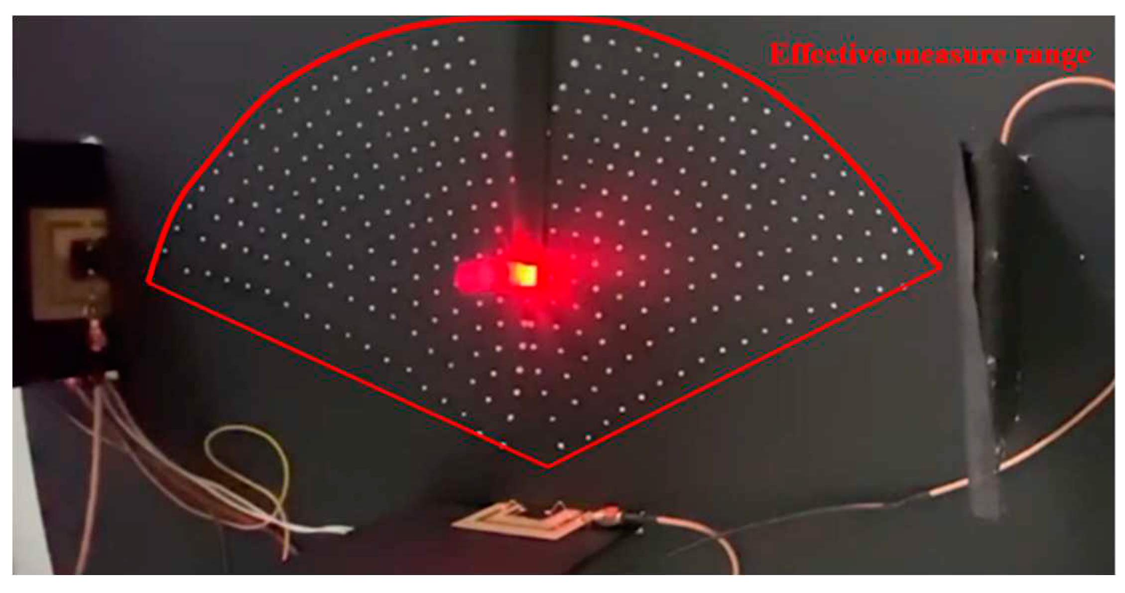
The three sensors were connected to the SR570 low-noise current preamplifier using SMA connectors. The amplified voltage signals were interfaced to LabVIEW software via a NI-9234 DAQ module. The positioning experiments were conducted using a high-power infrared source as the target object (Fig. 13). The voltage signals of the three sensors were first measured sequentially with the light turned off. The light was then turned on, and the voltage signals of the three sensors were measured once again. The precise position of the light source was determined using a trilateration approach based on the three voltage change measurements (Fig. 14). Finally, the coordinates of the light source were displayed as a plotted point on an X-Y graph presented through the LabVIEW HMI (Fig. 15).
Figure 13.
Experimental position measurement system.
Figure 13.
Experimental position measurement system.
Figure 14.
LabVIEW Mathscript position determination code.
Figure 14.
LabVIEW Mathscript position determination code.
Figure 15.
Human-machine interface showing coordinates of sensed target.
Figure 15.
Human-machine interface showing coordinates of sensed target.
Table 1 compares the measured coordinates of the infrared light source with the computed coordinates for three positioning tests. As shown, the average positioning error lies within ± 0.13 cm.
5. Conclusions
This study has presented a MEMs-based ZnO thin-film infrared sensor for non-contact temperature and distance sensing. The XRD results have shown that, following annealing at 500℃ for four hours, the ZnO film demonstrates a strong peak in the (002) crystallographic direction, indicating that it has a wurtzite structure. It has been shown that the ZnO sensor can function as an infrared-based target detection system over the range of 0 ~ 30 cm. A trilateration-based object localization system has been constructed based on three sensors and a self-written LabView interface. The experimental results have shown that the estimated target position deviates from the actual position by no more than 0.13 cm.
Author Contributions
Conceptualization and design, C.-Y. L.; methodology, C.-Y. T. and Y.-W. L.; fabrication and experiments, C.-Y. T. and Y.-W. L.; data analysis, C.-Y. L. and H.-M. K., writing, C.-Y. T., H.-M. K. and C.-Y. L. All authors have read and agreed to the published version of the manuscript.
Funding
This research was funded by the Ministry of Science and Technology in Taiwan, grant number MOST 110-2622-E-020-001.
Institutional Review Board Statement
Not applicable.
Informed Consent Statement
Not applicable.
Data Availability Statement
The data presented in this study are available on request from the corresponding author.
Conflicts of Interest
The authors declare no conflict of interest.
References
- Watton, R. Ferroelectric materials and devices in infrared detection and imaging. Ferroelectric 1987, 91, 87–108. [CrossRef]
- Ploss, B.; Bauer, S. Characterization of materials for integrated pyroelectric sensors. Sens. Actuator A Phys. 1991, 26, 407–411. [CrossRef]
- Hammes, P.C.A.; Regtien, P.P.L. An integrated infrared sensor using the pyroelectric polymer PVDF. Sens. Actuator A Phys. 1992, 32, 396–402. [CrossRef]
- Lienhard, D.; Nitschke, S.; Ploss, B.; Ruppl, W. The optimization of low cost integrated pyroelectric sensor arrays. Sens. Actuator A Phys. 1994, 41–42, 553–557. [CrossRef]
- Togami, Y.; Okuyama, M.; Hamakawa, Y. Pyroelectric infrared image sensors using Si CCD and FET arrays. Sens. Actuator A Phys. 1994, 40, 111–116. [CrossRef]
- Takayama, R.; Tomita, Y.; Iijima, K.; Ueda, I. Pyroelectric properties and application to infrared sensors of PbTiO3, PbLaTiO3, and PbZrTiO3 ferroelectric thin films. Ferroelectrics 1991, 118, 325–342.
- Choi, J.R.; Polla, D. Integration of microsensors in GaAs MESFET process. J. Micromech. Microeng. 1993, 3, 60–64. [CrossRef]
- Lienhard, D.; Heepmann, F.; Ploss, B. Thin nickel films as absorbers in pyroelectric sensor arrays, Microelectron 1995, 29, 101–104. [CrossRef]
- Hashimoto, K.; Yoshinomoto, M.; Matsueda, S.; Morinaka, K.; Yoshiike, N. Development of people-counting system with human-information sensor using multi-element pyroelectric infrared array detector. Sens. Actuator A Phys. 1997, 58, 165–171. [CrossRef]
- Chang, C.C.; Tang, C.S. An integrated pyroelectric infrared sensor with a PZT thin film. Sens. Actuator A Phys. 1998, 65, 171–174. [CrossRef]
- Liu, Z.; Lu, T.; Dong, X.; Wang, G.; Liu, Y. Ferroelectric ceramics for pyroelectric detection applications: A review. IEEE Trans. Ultrason. Ferroelectr. Freq. Control 2021, 68, 242–252. [CrossRef]
- Chong, N.; Chan, H.L.W.; Choy, C.L. Pyroelectric sensor array for in-line monitoring of infrared laser. Sens. Actuator A Phys. 2002, 96, 231–238. [CrossRef]
- Hsiao, C.C.; Huang, K.Y.; Hu, Y.C. Fabrication of a ZnO Pyroelectric Sensor. Sensors 2008, 8, 185–192. [CrossRef]
- Hsiao, C.C.; Huang, S.W.; Chang, R.C.Temperrature field analysis for ZnO thin-film pyroelectric devices with partially covered electrode. Sensors and Materials 2012, 24, 421–441.
- Wei, C.S.; Lin, Y.Y.; Hi, Y.C.; Wu, C.W.; Shih, C.W.; Huang, C.T.; Chang, S.H. Partial-electroded ZnO pyroelectric sensors for responsivity improvement. Sens. Actuator A Phys. 2006, 128, 18–24. [CrossRef]
- Liu, W.; Ko, J.; Zhu, W. Influences of thin Ni layer on the electrical and absorption properties of PZT thin film pyroelectric IR sensors. Infrared Phys. Technol. 2000, 41, 169–173. [CrossRef]
- Gaur, S.P.; Rangra, K.; Kumar, D. MEMS AlN pyroelectric infrared dector with medium to long wave IR absorber. Sens. Actuator A Phys. 2019, 300, 111660.
- Lee, C.Y.; Yu, C.X.; Lin, K.Y.; Fu, L.M. Effect of Substrate-Thickness on Voltage Responsivity of MEMS-Based ZnO Pyroelectric Infrared Sensors. Appl. Sci. 2021, 11, 9074. [CrossRef]
- Kim, S.Y.; Choi, J.Y. Indoor Positioning System using Incident Angle Detection of Infrared sensor. J. Inst. Control. Robot. Syst. 2010, 16, 991–996. [CrossRef]
- Gorostiza, E.M.; Zapata, F.E.; Infrared Sensor System for Mobile-Robot Positioning in Intelligent Spaces. Sens. 2011, 11, 5416–5438. [CrossRef]
- Luo, X.; Guan, Q. Simultaneous Indoor Tracking and Activity Recognition Using Pyroelectric Infrared Sensors. Sens. 2017, 17, 1738.
- Yan, J.; Lou, P. Research on the Multiple Factors Influencing Human Identification Based on Pyroelectric Infrared Sensors. Sens. 2018, 18, 604. [CrossRef]
- Agmell, S. IR-Based Indoor Localisation and Positioning System. Linköping University, Linköping, Sweden. 2019-06-05.
- Zhang, Q; Li, Y. Indoor Positioning Method Based on Infrared Vision and UWB Fusion. J. Phys.: Conf. Ser. 2021, 2078, 012070. [CrossRef]
- Wu, C.M.; Chen, X.Y.; Wen, C.Y.; Sethares, W.A. Cooperative networked PIR detection system for indoor human localization. Sensors 2021, 21, 6180–6202. [CrossRef]
- Whatmore, R.W. Pyroelectric devices and materials. Rep. Prog. Phys. 1986, 49, 1335–1386. [CrossRef]
|
Disclaimer/Publisher’s Note: The statements, opinions and data contained in all publications are solely those of the individual author(s) and contributor(s) and not of MDPI and/or the editor(s). MDPI and/or the editor(s) disclaim responsibility for any injury to people or property resulting from any ideas, methods, instructions or products referred to in the content. |
© 2023 by the authors. Licensee MDPI, Basel, Switzerland. This article is an open access article distributed under the terms and conditions of the Creative Commons Attribution (CC BY) license (http://creativecommons.org/licenses/by/4.0/).
