Introduction
Cerium dioxide is increasingly used in various high-tech industries: for the production of electrochemical elements [
1,
2,
3,
4,
5,
6,
7,
8], in photocatalysis [
9,
10], catalysis [
11,
12], to create new types of thermal barriers, heat-insulating materials [
13,
14,
15] and antireflection coatings for solar cells [
16], in optical devices [
17], etc. due to its high melting point and coefficient of thermal expansion, low thermal conductivity and valence transition Ce3+ - Ce4+. Cerium oxide has long been used as a polishing material due to its abrasive properties. The hydrophobicity of cerium oxide coatings is one of the key factors for its use in the development of new types of medical implants and other functional devices [
18]. Due to its relatively low toxicity, it is considered a potential replacement for chromium in anticorrosive protective coatings [
19]. Although it is noted as a neutral effect, and in some cases even a stimulating effect in experiments in vitro and in vivo, and unequivocally negative [
20]. It has been shown that the properties of cerium oxide depend on the size factor [
21], surface charge [
21], preparation method [
23,
24], and concentration [
25].
In this regard, research is underway on various methods for obtaining coatings from cerium oxide, including plasma chemical vapor deposition [
26], pulsed laser deposition [
27], and magnetron cathode sputtering [
28,
29,
30,
31,
32,
33,
34,
35,
36]. Magnetron sputtering allows you to create thinner coatings, while maintaining the properties and functions of thicker ones. The method makes it possible to obtain hardening, wear-resistant, protective, decorative and other types of coatings with a thickness of tens of nano- to hundreds of micrometers on products of various sizes (from millimeters to several meters) and configurations (plates, wire, complex three-dimensional shapes, etc.) practically from all materials. The deposited materials can be combined in various combinations. In this case, it is necessary to take into account a wide range of technological parameters and their relationship with the structure of the obtained materials.
One of the main problems in this case is the appearance in the composition of the coating, in addition to CeO2, of non-stoichiometric inclusions of Ce2O3, which leads to a decrease in mechanical, hydrophobic, and other properties; therefore, many modern works are aimed at finding the best methods that reduce/eliminate this process. One of such methods can be annealing following the deposition of a coating of metallic cerium or its oxides [
32,
33,
35,
36].
The aim of this work was to form layered composite materials with a surface layer of cerium dioxide based on the TIAL6V4 titanium alloy for medical use by magnetron sputtering and to study the effect of post-annealing on them.
Materials and methods
The creation of layered composite materials was carried out using a DC magnetron in an argon gas environment at a Torr International facility (USA).
The use of magnetron sputtering to create surface layers makes it possible to avoid overheating of the substrate by bombarding electrons due to their retention at the sputtered target, which is extremely important for substrate materials with low melting temperatures or a phase structure sensitive to temperature changes, such as, for example, superelastic titanium alloys - heat treatment makes it possible to vary static properties and cyclic loading under operating conditions with a wide range of deformations and is extremely important for the stabilization of properties, molding of products and successful application of the product.
Discs made of chemically pure cerium were used as a sputtered target. Due to the active oxidation of cerium in an oxygen-containing medium, before each deposition, the target surface was cleaned, incl. using ion etching. As a basis for the composites, plates made of titanium alloy TIAL6V4 with a size of 10 × 10 × 0.5 mm were used. The plates were pretreated for 5 min with Polinox (Dzhitul, Russia), which is a mixture of nitric, hydrofluoric, and sulfuric acids in glycerin. For cleaning, activation and polishing, the surface of the substrate before deposition was bombarded with argon ions for 3 min at voltage and current, respectively, Ue = 900 V and Ie = 80 mA - preliminary ion etching.
Surface layers were obtained under the following process conditions: 1) I ~ 135–865 mA, U ~ 323–347 V (power supply power ≈ 43–300 W, which corresponds to the range indicated in this work as 10–70%); 2) deposition time t = from 5 to 30 min; 3) spraying distance (distance from the target to the substrate) 150 mm. The temperature on the substrate surface did not exceed 150°C. The working and residual pressure in the vacuum chamber were ~ 0,4 and 4х10-4 Pa, respectively. Ten minutes after the deposition of metallic cerium, the atmosphere of the chamber was saturated with oxygen. After waiting 2 days after deposition to naturally remove the activation of the newly formed surface, half of the samples were annealed in an oxygen-containing environment at a temperature of 400°C.
The morphology and layer-by-layer elemental composition of the surface of the materials were studied on a Hitachi TM4000 scanning electron microscope (SEM) (Japan) equipped with an attachment for energy dispersive analysis (EDA), a JAMP-9500F electron Auger spectrometer (JEOL, Japan) in combination with ion etching under argon bombardment. at an angle of 30°. X-ray diffraction patterns (XRD) were obtained on a DRON-3M device (Burevestnik, Russia), in CoKα radiation in a parallel beam geometry.
Hardness measurement was carried out by sclerometry, which consists in analyzing the profile of scratches applied to the surface of the material, the hardness of the test material is determined relative to the known hardness of the standard sample (SD) by the ratio of loads and widths of scratches obtained on the test and standard samples. The measurements were carried out on a nanohardness tester NanoScan-3D (TISNUM, Russia), using a trihedral Berkovich pyramid, at loads of 60 mN. Each sample was covered with a series of 60 scratches, each of which was 50 µm in length. An array of scratches was necessary in view of the significant (up to 1.5 μm) height differences on the samples. The relief and topography of the surface of the samples were studied by atomic force microscopy on the Solver Pro M complex (NT-MDT, Russia) by the semi-contact method.
Results and discussion
Immediately after magnetron deposition, depending on the variable parameters (sputtering time and power), surface layers of cerium dioxide were obtained with a thickness from tens to thousands of nanometers (
Table 1). A linear increase in the length of the layer was observed with an increase in the deposition time at any power, while with an increase in power within one deposition time, an extreme dependence was observed - at first, the thickness of the layers increased, and at 30% a high sputtering rate of the material (38 nm/min) was achieved, at At higher power, the intensity of the flux of particles emitted from the target naturally increased, however, a gradual decrease in the thickness of the surface layers was observed. The cause of this phenomenon was assumed to be self-sputtering of the freshly deposited material, when, simultaneously with the deposition process, cerium is etched from the surface of the composite by its own atoms and ions, similar to the process of ion etching [
37].
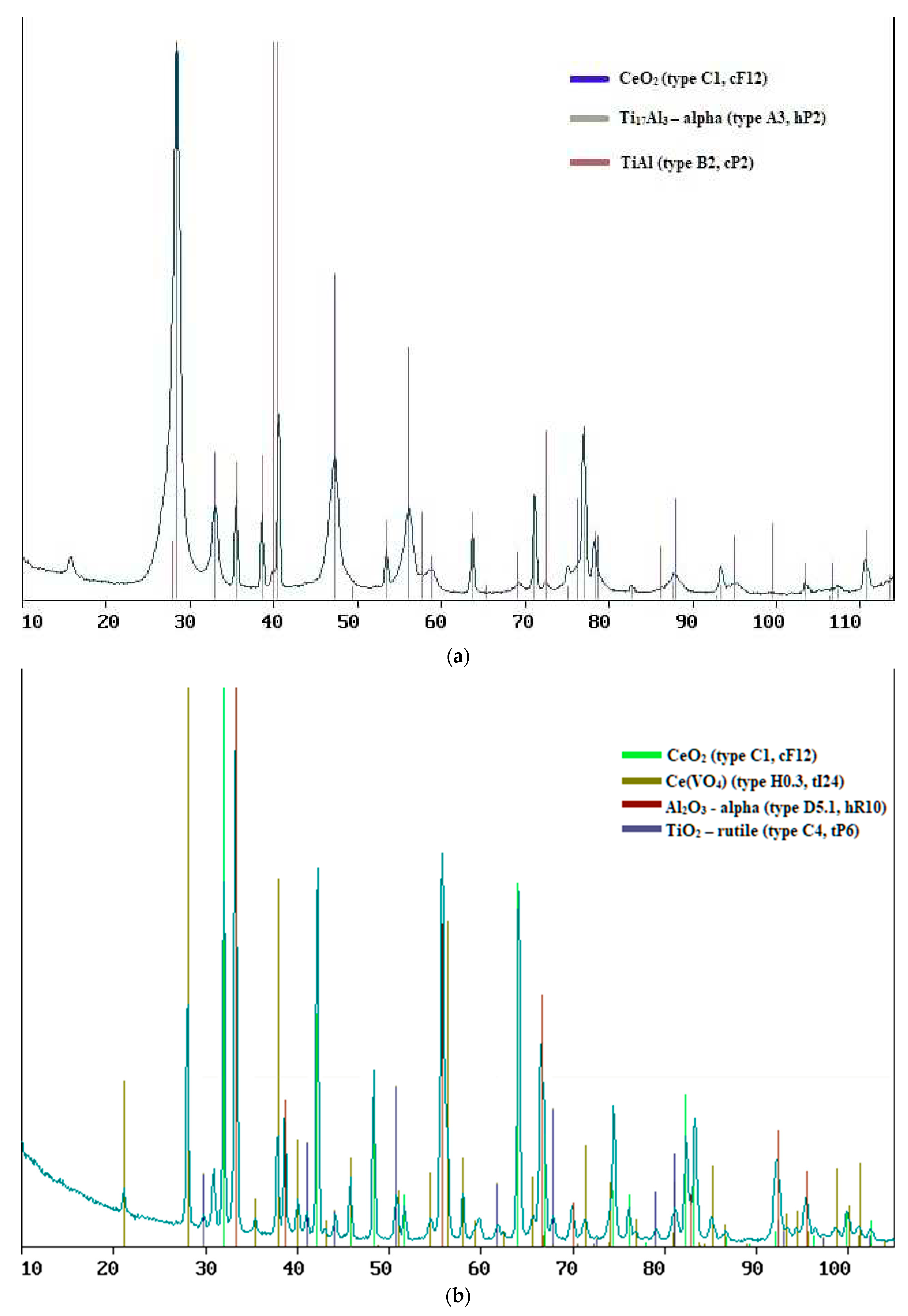
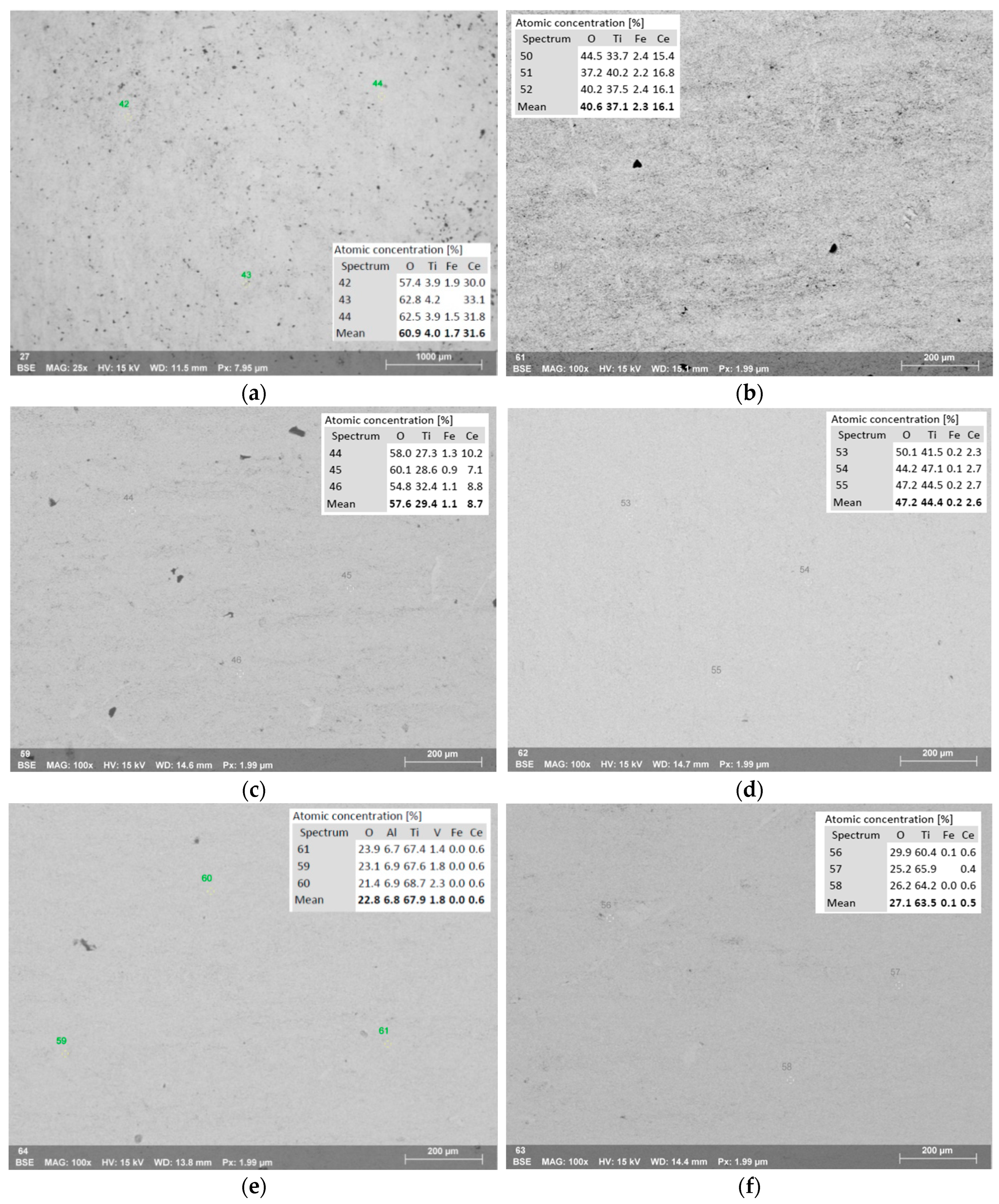
Regardless of the sputtering conditions, it was noted that with a cerium dioxide layer thickness of less than 715 nm, the presence of titanium, aluminum and vanadium oxides was observed in the samples of composite materials, which were not present at a longer layer length (
Table 1,
Figure 1 and
Figure 2). It was assumed that the oxides of other metals form a sublayer under CeO
2 if the thickness of the latter allows excess oxygen to diffuse into the substrate. Regardless of the deposition conditions, cerium immediately after magnetron sputtering forms stoichiometric dioxide, in the form of an independent layer corresponding in phase composition to a set of diffraction peaks at 2θ values of 28.61°, 33.14°, 47.57°, 56.35°, 59.13 ° etc., which corresponds to (111), (200), (220), (311), (222), etc. planes of a cubic structure of the fluorite type with space group Fm3m (
Figure 1).
The CeO
2(111) orientation is the most expected, since it has the most thermodynamically stable state. In most cases, a deviation from the orientation of the resulting CeO
2(111) coating is observed when the stoichiometric ratio of Ce
4+ and O
2– is violated. In this case, due to the loss of oxygen, the Ce
4+ - Ce
3+ phase transition occurs, amorphous Ce
2O
3 is formed at the grain boundaries or around CeO
2 oxygen vacancies, and crystalline Ce
2O
3 is further formed. The appearance of Ce
2O
3 in the composition of the coating leads to a decrease in mechanical, hydrophobic, and other The work is aimed at finding the best parameters for magnetron sputtering that reduce/eliminate this process. Usually, in the absence of oxygen in the atmosphere of the working chamber, immediately at the moment of sputtering of a pure Ce target, the resulting pure cerium coating, after being removed from the installation, immediately oxidizes to a mixture of CeO
2(111), CeO
2 (200), and Ce
2O
3 [
30]. However, the supply of oxygen during the sputtering process contributes to the rapid clogging of the target itself with oxygen, since cerium is extremely prone to react with oxygen, which presents a number of difficulties for the DC magnetron sputtering process. In our case, the amount of oxygen admitted into the chamber after deposition, when cerium itself is in the activated state, was sufficient to prevent the formation of Ce
2O
3.
As the layer thickness increases (
Figure 2), a barely noticeable folded relief appears on the surface, and at the maximum thickness, point defects can be observed, which can just be traces of local bombardment by high-energy particles of sputtered cerium.
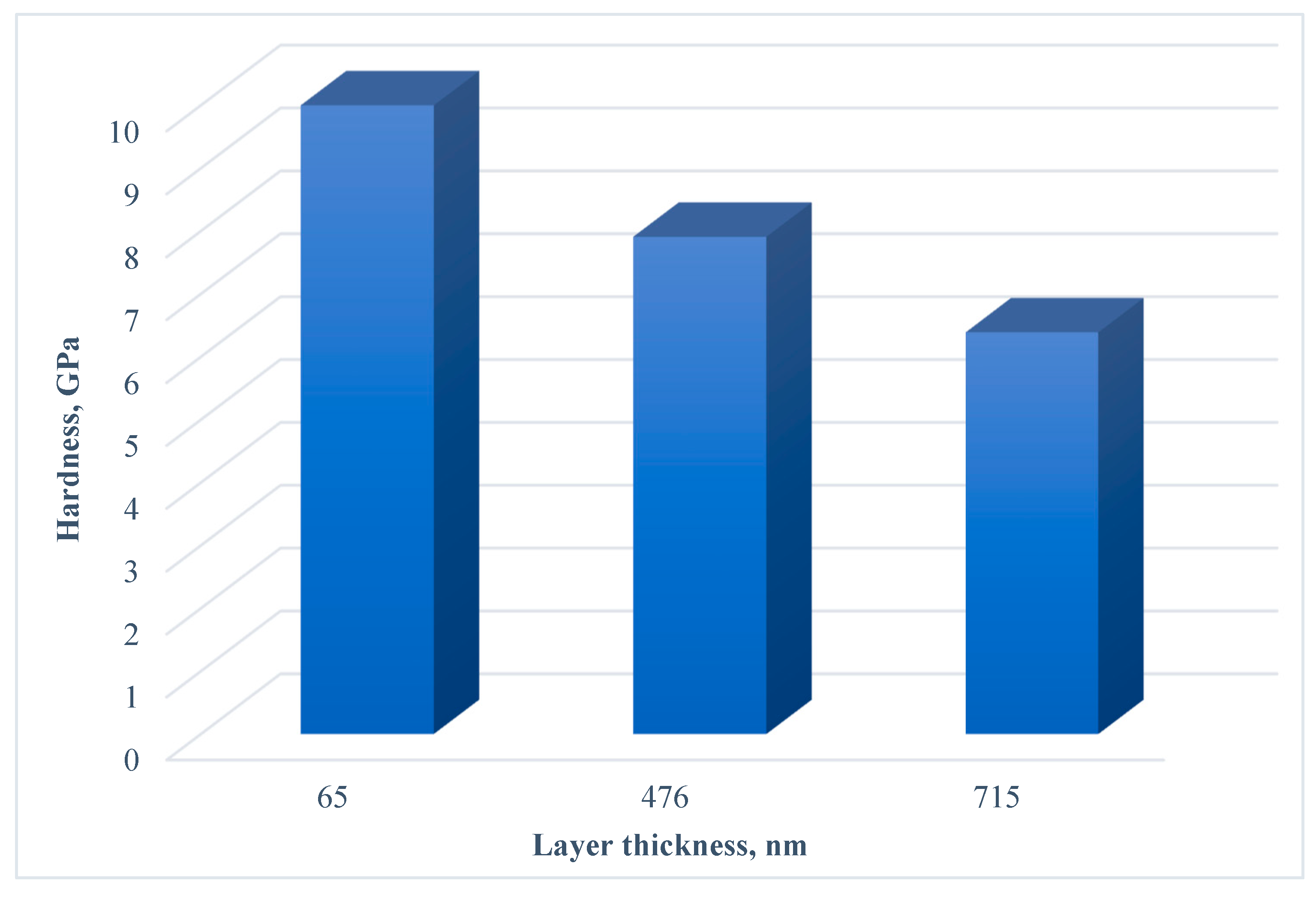
When analyzing the hardness of unannealed samples with different thicknesses of the surface layers of cerium dioxide (the samples were compared with a sublayer of titanium, aluminum, and vanadium oxides) by sclerometry (
Figure 3), an increase in the index was noted with a decrease in the coating thickness. During the formation of cerium oxide layers on silicon and ceramics, it is noted that the highest hardness values are achieved at the maximum content of the fine-grained dense CeO
2 (111) crystalline phase and high compressive stress [
29,
32,
36]. Perhaps, as the layer thickness increases, stress relaxation and/or grain growth occurs, since at a higher flow intensity and deposition time, a greater local heating of the sample surface naturally occurs.
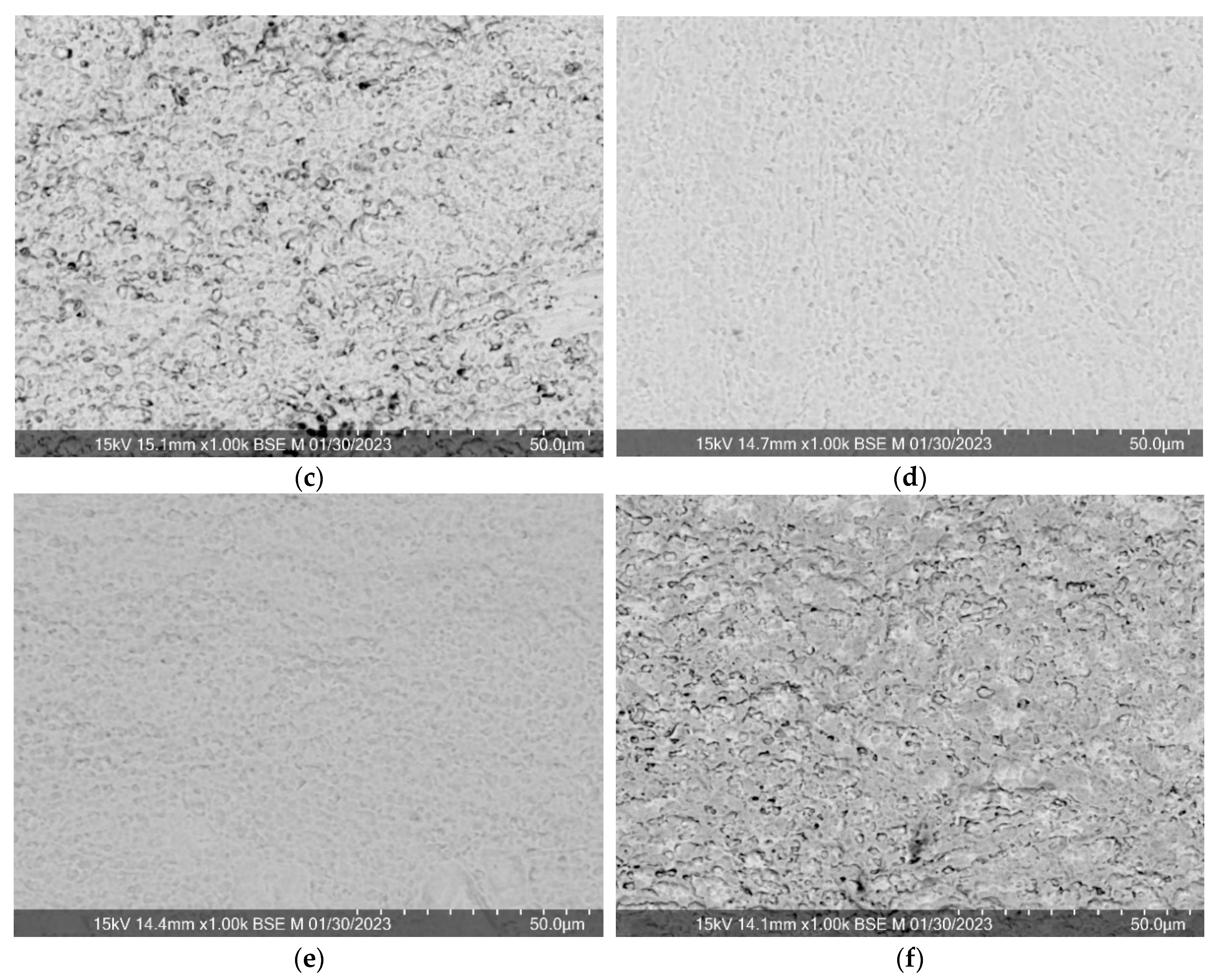
Regardless of the sputtering conditions, the surface morphology of the formed composite materials repeats the substrate surface morphology (
Figure 4). However, it can be noted that after 5 minutes of deposition at a power of 25%, rare and hardly noticeable folds appear, probably due to compressive stress, and after 20 minutes at 50%, the elements of the initial relief become coarser, it looks smoother, which is consistent with the assumption of self-spraying. Surface layer by high-power flows of the deposited substance.
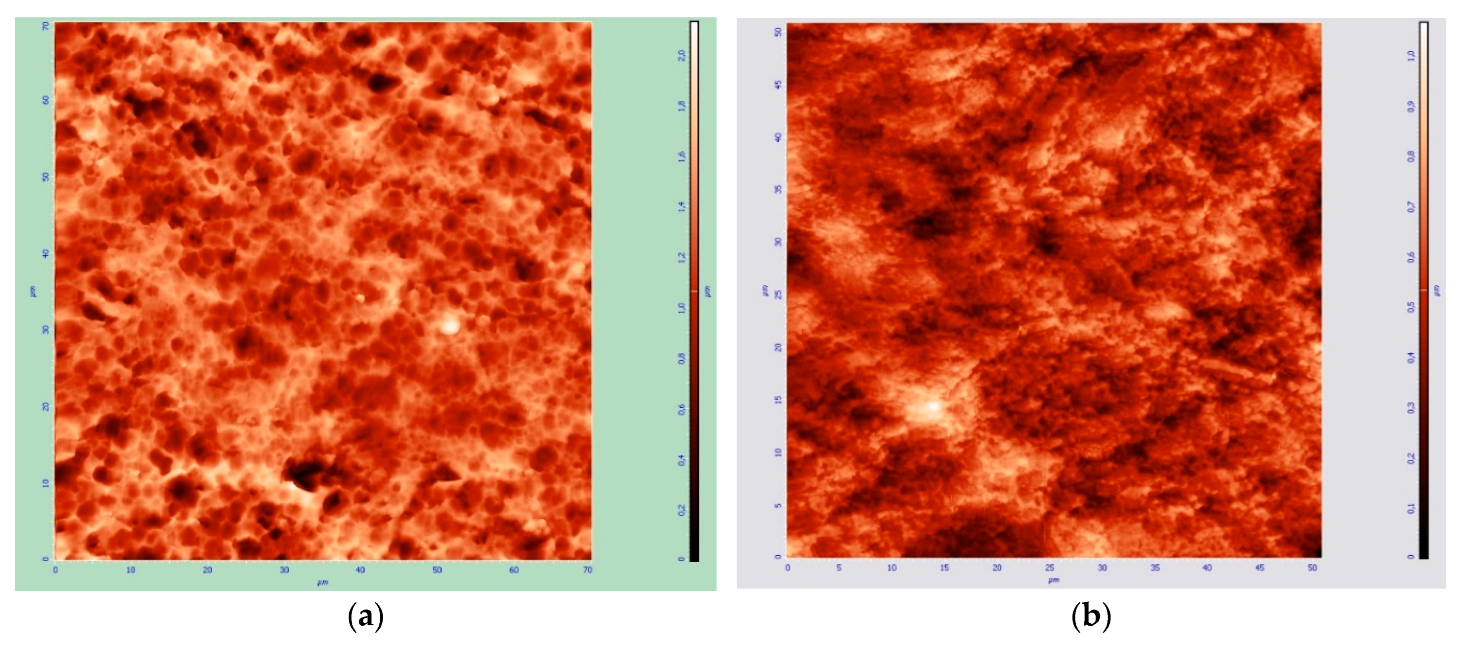
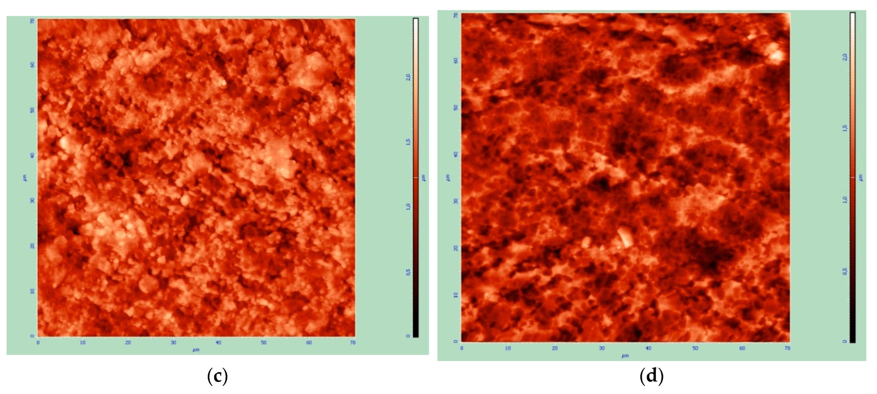
The topography of the surface of samples with thin surface layers of cerium dioxide after sputtering is shown in
Figure 5. It can be noted that an increase in thickness from 65 nm to 120 nm due to an increase in sputtering power leads to a decrease in relief elements – hillocks and depressions (both in height and in in diameter), as if they were compressed, with an increase in thickness to 160 nm, the surface elements again become coarser and deform even more, and the roughness increases, and at 480 nm the surface becomes similar to the original, but with more sharply defined details, while the spread of the surface in height becomes less.
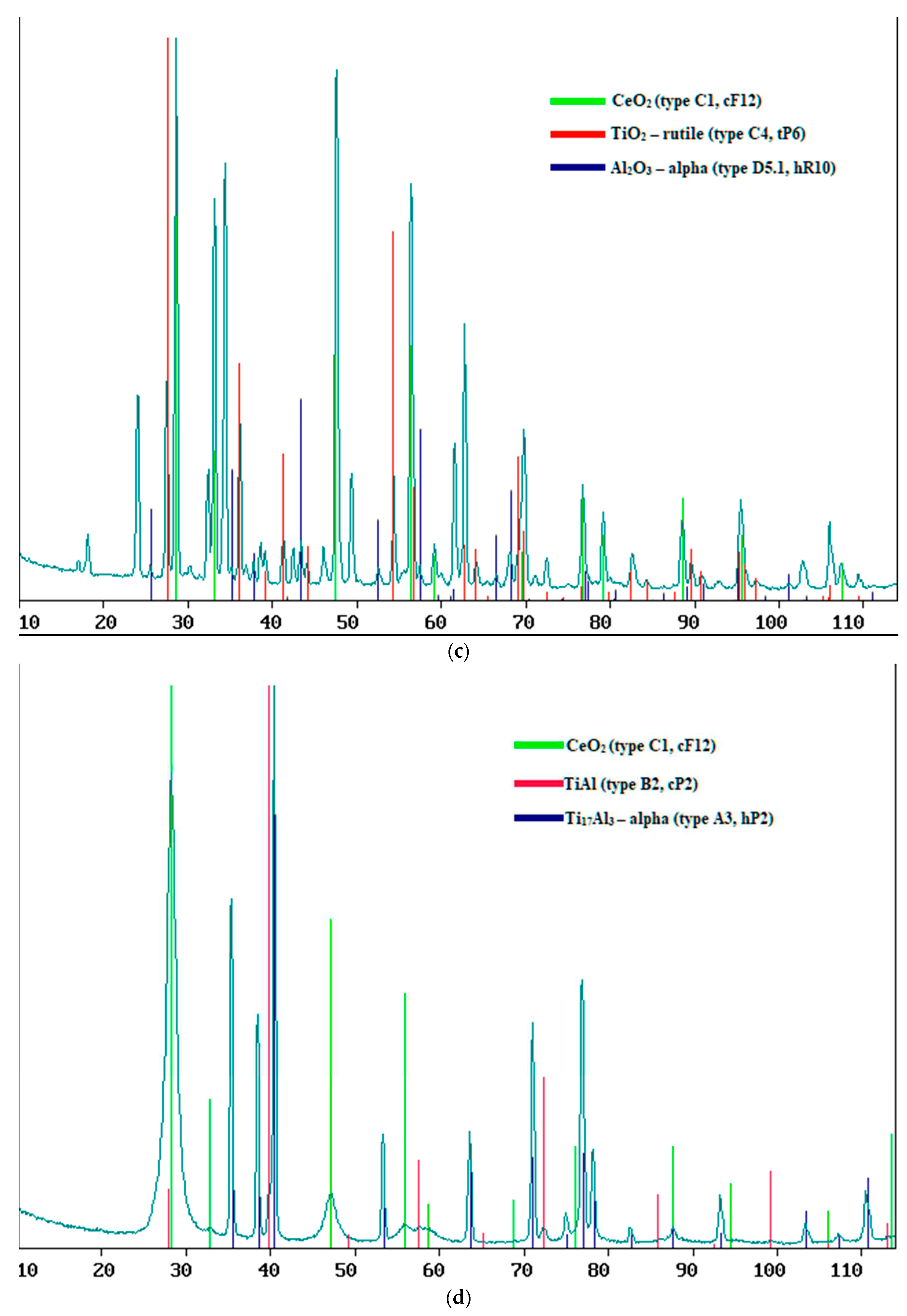
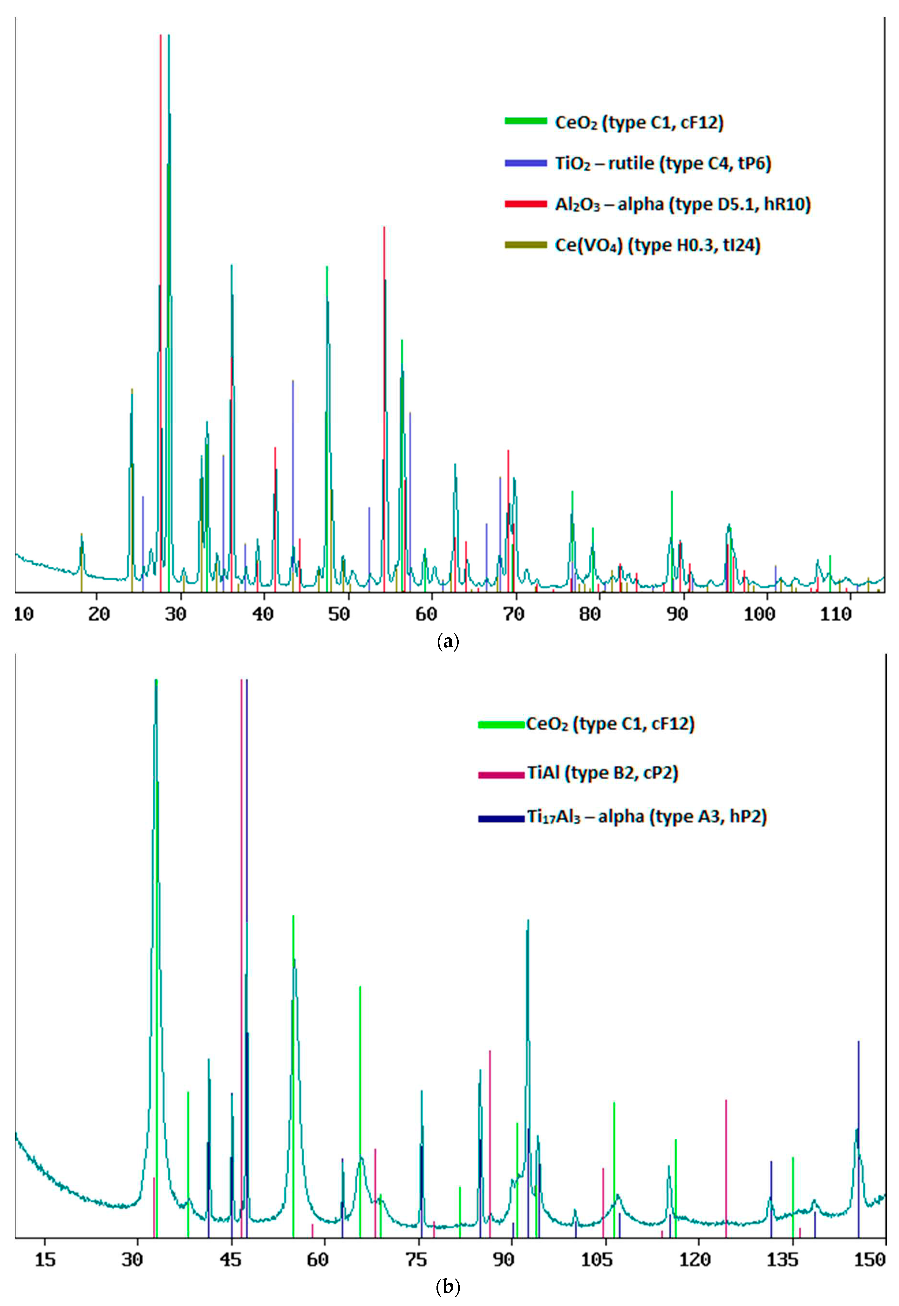
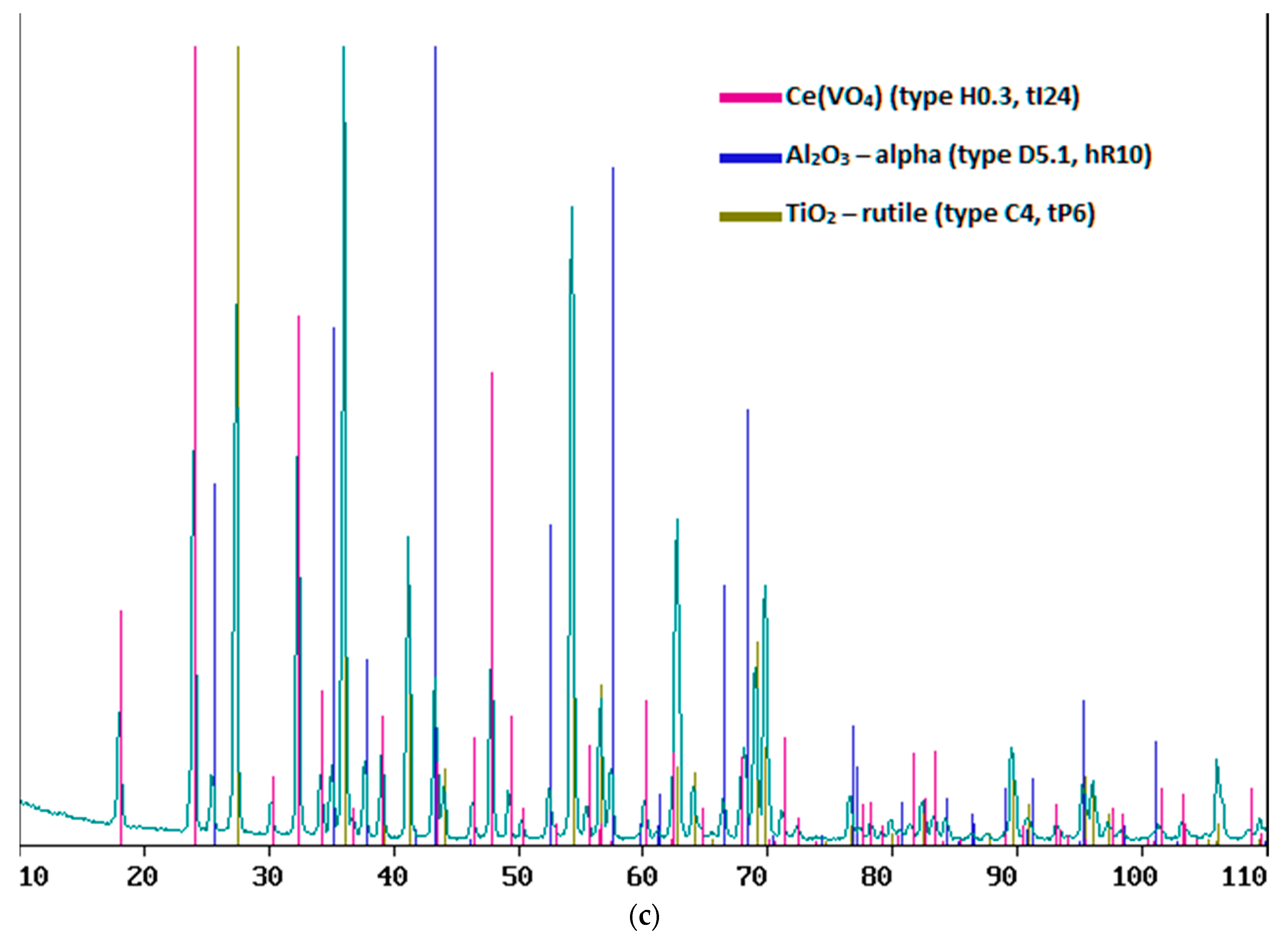
After annealing at low power, surface layers of cerium dioxide were obtained with a thinner thickness than without it; at 50% power, the thicknesses of the layers obtained without post-annealing and with it were close, but slightly higher after annealing, and at 70% annealing significantly increased the thickness layers (
Table 2). It was noted that, at a surface layer thickness of less than 790 nm, in addition to cerium dioxide, metal oxides of the substrate are formed in the form TiO
2, Al
2O
3 and Ce(VO
4), which were absent at a longer layer length, and at a layer length of less than 300 nm, all cerium dioxide is spent on combining with vanadium dioxide to form vanadate (
Figure 6).
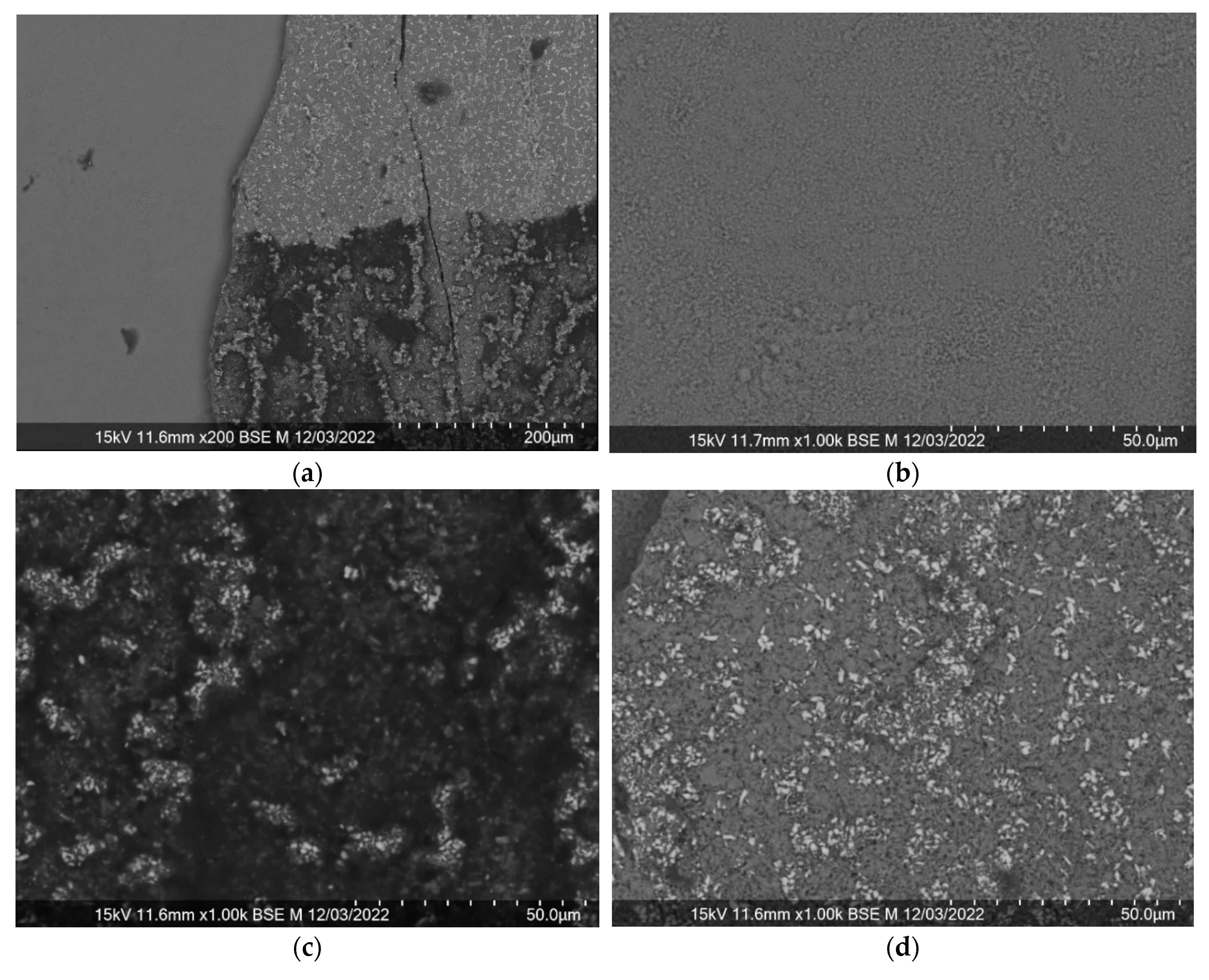
Figure 7 shows the delamination of the resulting surface into 3 different areas, for each of which the chemical composition was checked, as a result of which the zones were defined as the substrate, the top layer of cerium dioxide and the mixed oxide layer between them.
In this case, a linear increase in the length of the layer was also observed with an increase in the deposition time at any power. With an increase in power within one deposition time, the thickness of the surface layer also increased, however, with strong deviations from the linear regularity. Since defects in the surface were observed on many samples, peeling of small (micron) and rather large (millimeter) sections of the surface layer (
Figure 7), thickness fluctuations from the general pattern can be explained by the loss of part of the coating. At the same time, surface loosening after relaxation and recrystallization caused by annealing [
29,
32,
36] can also explain the increase in the imaginary thickness of the surface layer. For example, in
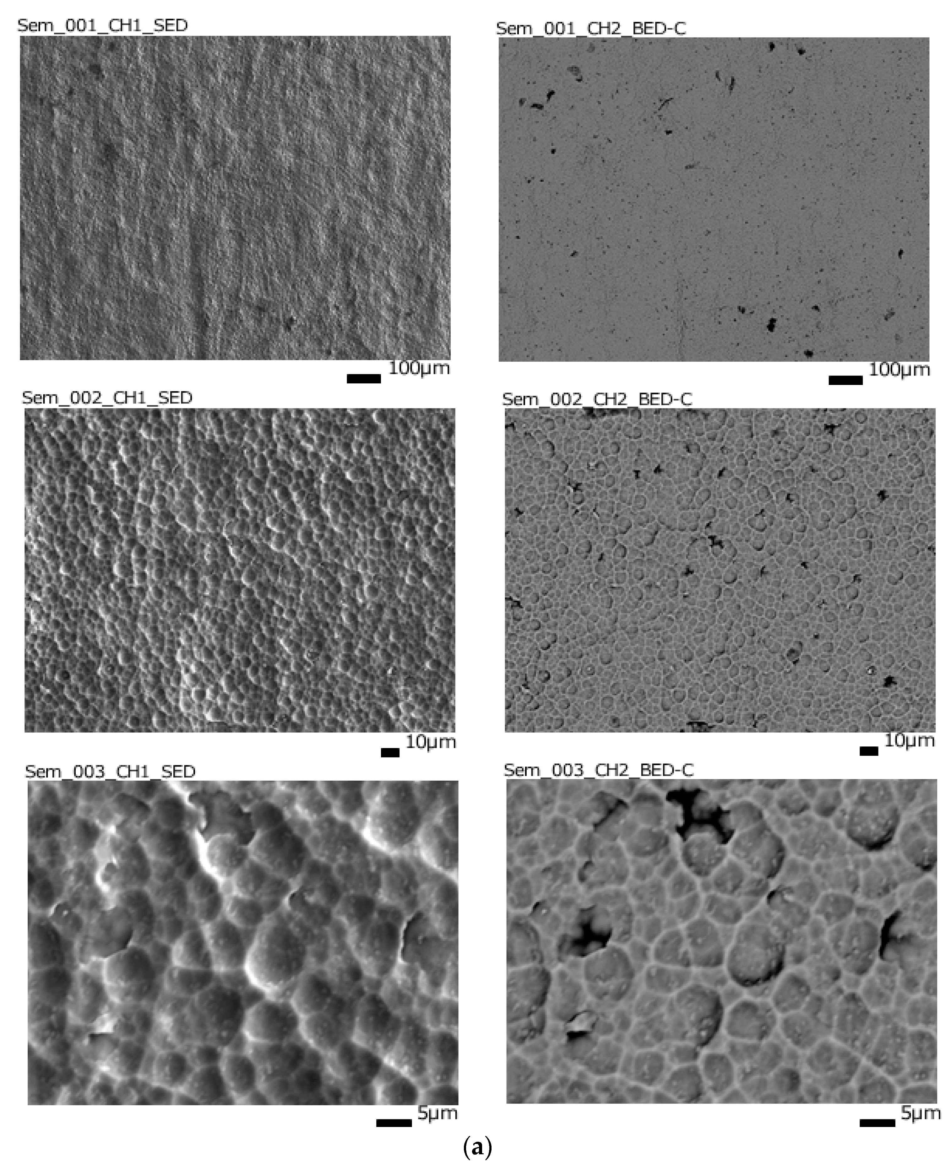
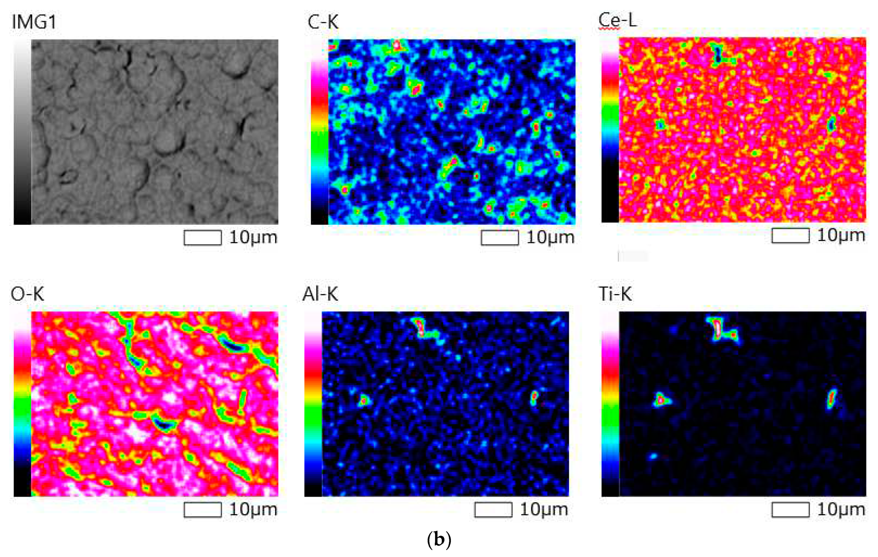
Figure 8, loose pores can be observed through the entire surface layer of almost micron thickness to the substrate.
It is also noted that an increase in the amount of oxygen affects the size of the resulting grain СеО
2, including grain refinement and roughness increase [
30,
34,
35,
36], which we can see in
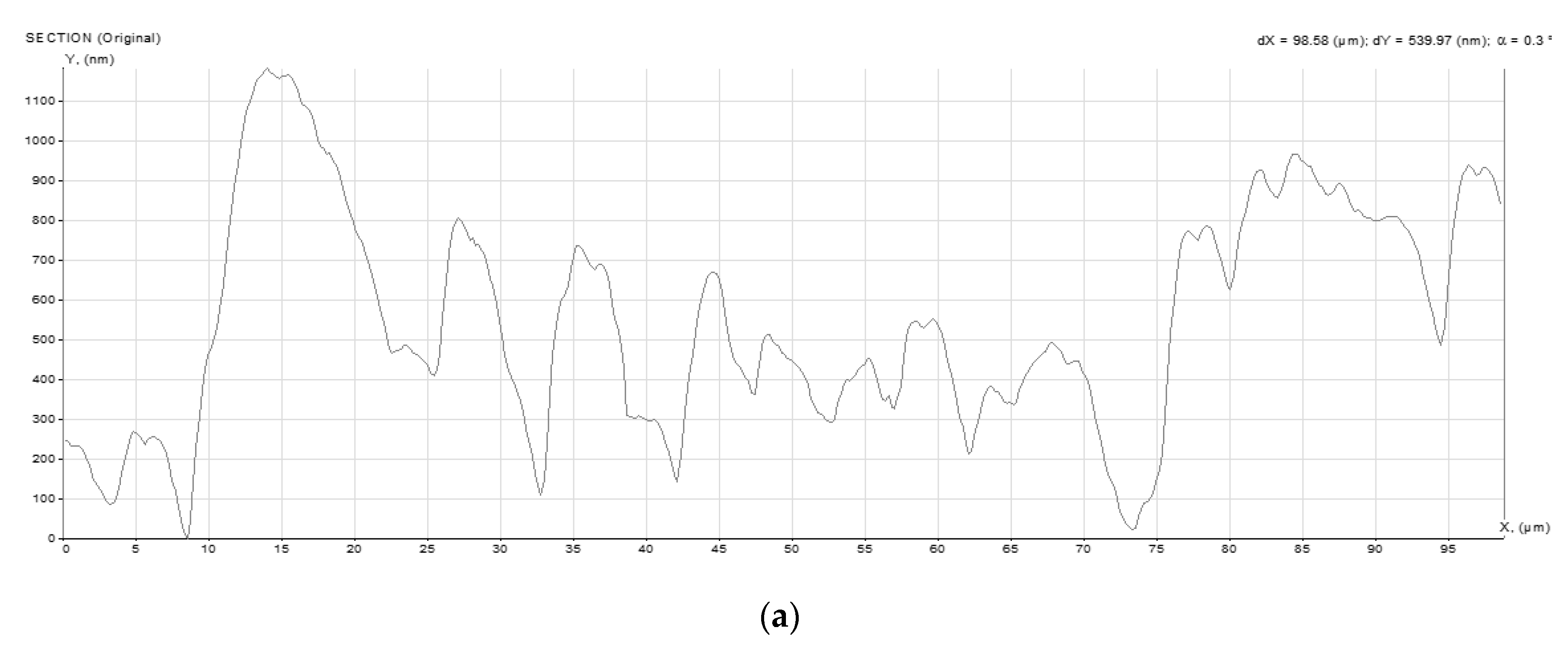
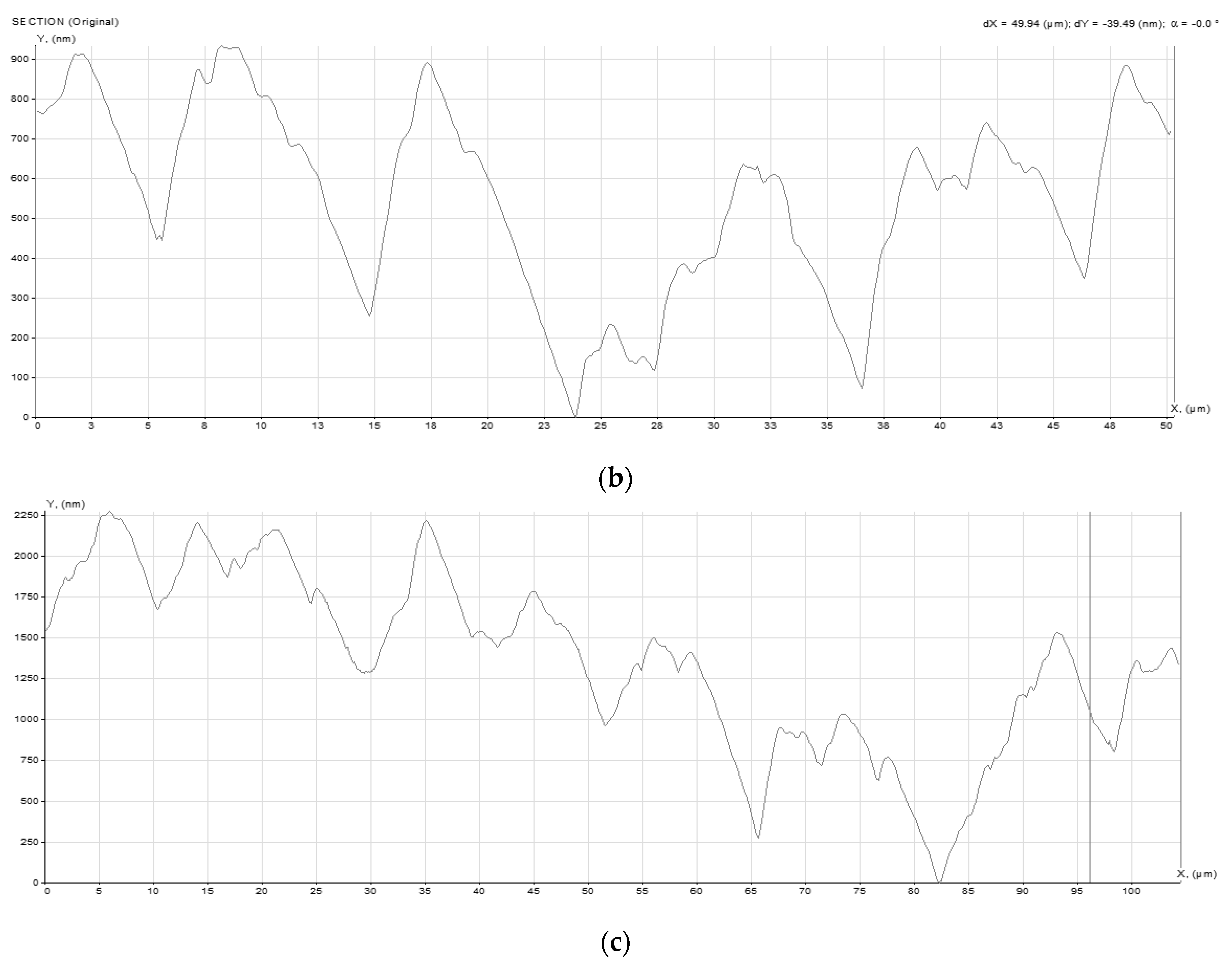
Figure 9, while high roughness in the case of thin surface layers significantly affects the analysis results. The surface layer of almost 500 nm in the absence of annealing slightly smoothes the roughness of the original substrate.
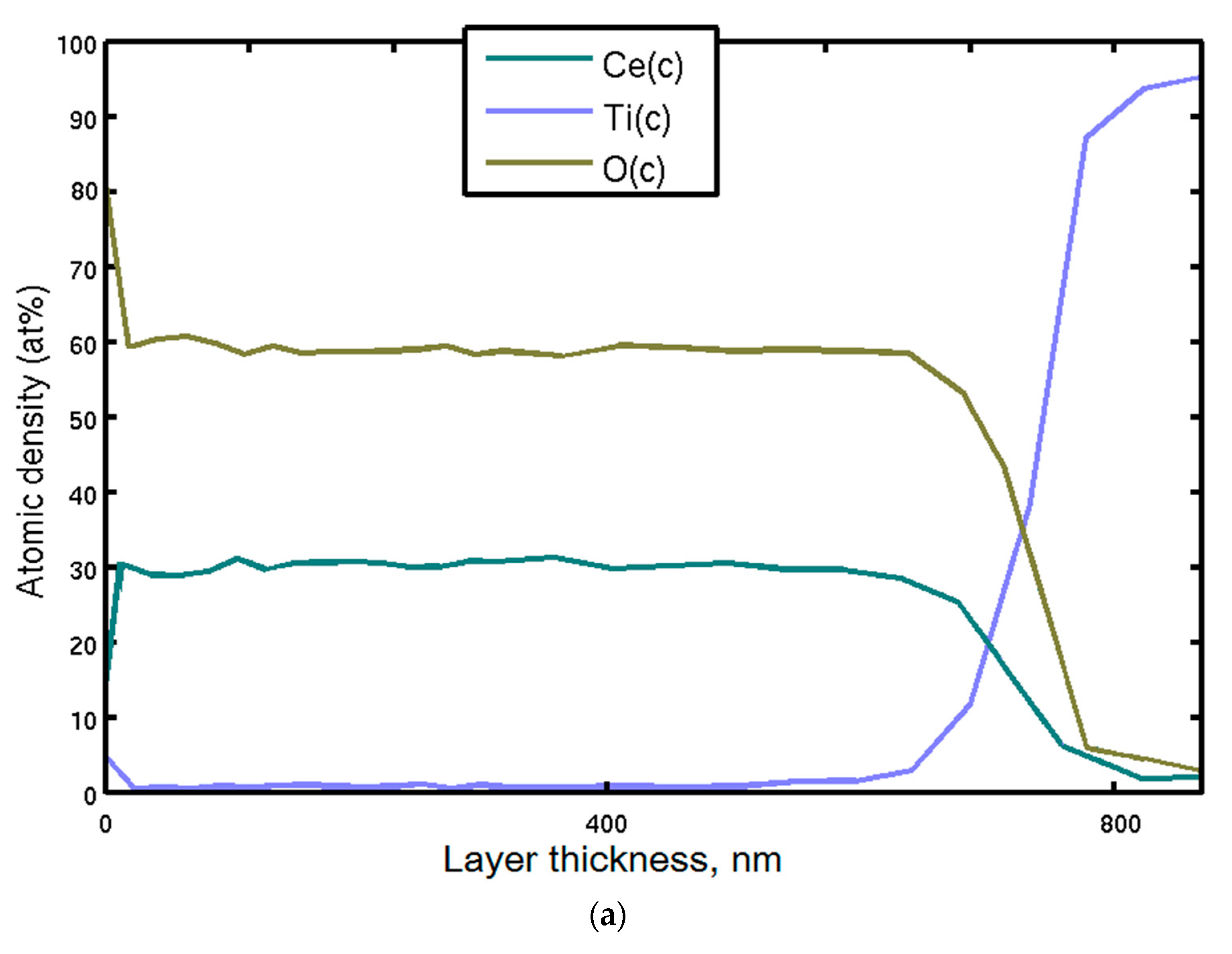
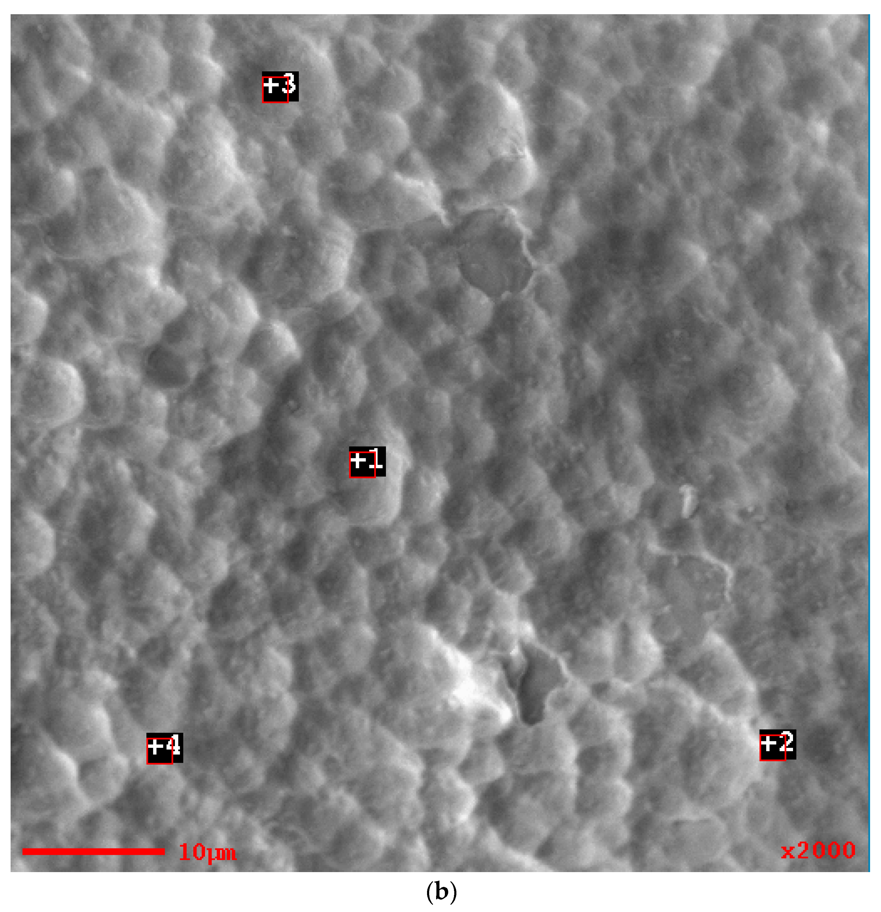
The layer-by-layer chemical composition and surface morphology of the composite material without a sublayer of oxides of other metals are shown in
Figure 10. The results of the chemical analysis showed high convergence at all points of the analysis.
Thus, in general, annealing following the deposition of cerium oxide showed unsatisfactory results and is not recommended as a stage in the technology for obtaining stoichiometric cerium dioxide.
Conclusions
Layered composite materials with surface layers of cerium dioxide of stoichiometric composition with a thickness of 35 to 1142 nm and a base of titanium alloy TIAL6V4 were obtained by magnetron sputtering.
A linear dependence of the thickness of the surface layer on the time of its deposition is noted, regardless of the presence or absence of subsequent annealing after deposition.
In the absence of annealing, a linear increase in the length of the layer was noted with an increase in power up to approximately 130 W, followed by its decrease. And if it is present, a nonlinear increase in the length of the layer with an increase in power, an increase in surface roughness, delamination and loosening of the surface layer.
In samples with a surface layer thinner than 715–750 nm, the formation of a sublayer of TiO2, Al2O3, and Ce(VO4) was found, and with a layer length of less than 300 nm, in the case of annealed samples, all cerium dioxide is spent on combining with vanadium dioxide to form vanadate.
The hardness of the samples, according to the sclerometry method, decreased with an increase in the thickness of the cerium dioxide layer.
Figure 1.
XPA results for samples of composite material “CeO2 – TiAl6V4”, obtained at: a) at 50% power for 30 min, b) at 70% power for 30 min, c) at 50% power for 20 min, d) at 20% power for 30 min.
Figure 1.
XPA results for samples of composite material “CeO2 – TiAl6V4”, obtained at: a) at 50% power for 30 min, b) at 70% power for 30 min, c) at 50% power for 20 min, d) at 20% power for 30 min.
Figure 2.
SEM results with EDA for samples of composite material “CeO2 – TiAl6V4”, obtained at: a) at 30% power for 30 min, b) at 20% power for 30 min, c) at 30% power for 12.5 min, d) at 25% power for 5 min, e) at 20% power for 5 min, f) at 10% power for 5 min.
Figure 2.
SEM results with EDA for samples of composite material “CeO2 – TiAl6V4”, obtained at: a) at 30% power for 30 min, b) at 20% power for 30 min, c) at 30% power for 12.5 min, d) at 25% power for 5 min, e) at 20% power for 5 min, f) at 10% power for 5 min.
Picture 3.
Hardness of composite material «CeO2 - TiAl6V4» samples.
Picture 3.
Hardness of composite material «CeO2 - TiAl6V4» samples.
Figure 4.
Morphology of the surface of the samples of the composite material “CeO2 – TiAl6V4”, obtained at: a) at 50% power for 20 min, b) at 10% power for 5 min, c) at 30% power for 12.5 min, d a) at 25% power for 5 minutes, e) at 20% power for 30 minutes, and f) the original substrate.
Figure 4.
Morphology of the surface of the samples of the composite material “CeO2 – TiAl6V4”, obtained at: a) at 50% power for 20 min, b) at 10% power for 5 min, c) at 30% power for 12.5 min, d a) at 25% power for 5 minutes, e) at 20% power for 30 minutes, and f) the original substrate.
Figure 5.
Surface topography of composite material samples «CeO2 – TiAl6V4», obtained at: a) at 10% power for 5 min, b) at 20% power for 5 min, c) at 25% power for 5 min, d) at 30% power for 12.5 min.
Figure 5.
Surface topography of composite material samples «CeO2 – TiAl6V4», obtained at: a) at 10% power for 5 min, b) at 20% power for 5 min, c) at 25% power for 5 min, d) at 30% power for 12.5 min.
Figure 6.
XRF results for samples of composite material “CeO2 – TIAL6V4”, obtained at: a) at 50% power for 20 min, b) at 50% power for 30 min and c) at 30% power for 12.5 min.
Figure 6.
XRF results for samples of composite material “CeO2 – TIAL6V4”, obtained at: a) at 50% power for 20 min, b) at 50% power for 30 min and c) at 30% power for 12.5 min.
Figure 7.
SEM results for a sample of the composite material «CeO
2 – TIAL6V4», obtained at 50% power for 20 min: a) general view of the delaminated material, b) c) and d) - 3 analysis zones:.
| Surface area |
Atomic content of the element, % |
| О |
Al |
Ti |
V |
Ce |
| b |
68,9 |
6,1 |
25,1 |
- |
- |
| c |
60,4 |
11,3 |
19,6 |
2,0 |
2,3 |
| d |
65,24 |
- |
2,76 |
1,06 |
29 |
Figure 8.
SEM image of the surface (a) and elemental mapping results (b) for a composite material sample «CeO2 – TIAL6V4», obtained at 70% power in 30 min.
Figure 8.
SEM image of the surface (a) and elemental mapping results (b) for a composite material sample «CeO2 – TIAL6V4», obtained at 70% power in 30 min.
Figure 9.
Surface profile of the original substrate (a) and samples of the composite material “CeO2 – TiAl6V4”, obtained at 30% power 12.5 min before (b) and after annealing (c).
Figure 9.
Surface profile of the original substrate (a) and samples of the composite material “CeO2 – TiAl6V4”, obtained at 30% power 12.5 min before (b) and after annealing (c).
Figure 10.
The profile of the distribution of elements in depth in the surface area of the sample of the composite material "CeO2 - TIAL6V4", obtained at 50% power for 30 min (a) and SEM of the analyzed area (b).
Figure 10.
The profile of the distribution of elements in depth in the surface area of the sample of the composite material "CeO2 - TIAL6V4", obtained at 50% power for 30 min (a) and SEM of the analyzed area (b).
Table 1.
Characteristics of the obtained samples of the composite material "CeO2 - TiAl6V4" according to XRD and SEM.
Table 1.
Characteristics of the obtained samples of the composite material "CeO2 - TiAl6V4" according to XRD and SEM.
| Sputtering time, min |
Sputtering power, % |
| 10 |
20 |
25 |
30 |
50 |
70 |
| Cerium dioxide layer thickness, nm |
| 30 |
390* |
715 |
960 |
1142 |
781 |
609* |
| 20 |
|
|
|
|
501* |
|
| 12,5 |
|
|
|
476* |
|
|
| 5 |
65* |
120* |
160* |
190* |
132* |
105* |
Table 2.
Characteristics of the obtained composite material samples «CeO2 – TIAL6V4» after annealing according to XRD and SEM.
Table 2.
Characteristics of the obtained composite material samples «CeO2 – TIAL6V4» after annealing according to XRD and SEM.
| Magnetron sputtering time, min |
Sputtering power, % |
| 20 |
30 |
50 |
70 |
| Cerium dioxide layer thickness, nm |
| 30 |
210** |
703* |
790 |
943 |
| 20 |
|
468,8* |
516* |
|
| 12,5 |
|
293** |
326* |
|
| 5 |
35** |
120** |
132** |
157** |
