1. Introduction
Due to the energy crisis caused by the problem of global warming, energy saving and carbon reduction become much more important. Renewable energy applications, including solar, wind or fuel cells, are thus emphasized because they have zero carbon emissions. For a single-phase 220 Vac generated from a DC-AC inverter in a distributed power grid system with renewable energy, a high dc voltage of 380~420 V is required to offer to the inverter. However, the output voltage of a solar array module is about 36 ~ 48 V for domestic applications, so a step-up DC-DC converter with a high voltage gain is needed to convert the voltage level.
In general, the ideal traditional boost DC-DC converter with a near unity duty cycle can achieve high voltage gain, but the presence of parasitic resistances in circuit components greatly limits the voltage gain and conversion efficiency [
1]. Therefore, for obtaining a high voltage gain and improving the conversion efficiency, many high step-up techniques have been presented and applied to propose a lot of high step-up converter structures [
2,
3,
4,
5,
6,
7,
8,
9,
10,
11,
12,
13,
14,
15,
16,
17,
18,
19,
20,
21,
22,
23,
24,
25,
26].
Switched-capacitor techniques [
2,
3,
4,
5,
6,
7] and voltage-lift techniques [
8,
9,
10,
11,
12,
13,
14,
15,
16] have been widely used to achieve high step-up voltage gain. The main purpose for these step-up techniques is to create voltages across the capacitors. Therefore, the induced capacitor voltages can be positively series at output side for a very high output voltage, but some of the high step-up converters [
3,
8,
17] have the drawback of no common ground involving the load, switches, and the input voltage source in order to cascode the voltages from the equivalent circuit structure deformed by component displacement. On the other hand, the capacitor voltages can also be set as a negative voltage against output voltage in the path of releasing energy for the inductor when the switch is off to be able to derive a much higher output voltage based on volt–second balance principle to inductors. However, if the voltage gain needs to be increased in advance, much more diodes and capacitors will be required and result in more cost and power losses. On the other hand, the high charging currents will also exist and flow through the main switches and rectified diodes, and that will increase more power dissipation.
In order to increase the voltage conversion ratio of a dc–dc converter, the other common solution is to use the turns ratio of the coupled inductor or transformer [
17,
18,
19]. These high step-up converters have an extra design freedom degree, which is the turns ratio. High voltage gain can thus be achieved for these converters with high turns ratio. However, a large turns ratio increases leakage inductance, which may cause high voltage spikes and increases voltage stresses on the switches and diodes. Therefore, several non-isolated converters have been proposed, such as switched-inductor applications [
20,
21,
22,
23,
24,
25,
26].
In [
26], a symmetrical dual-switch converter with synchronous switching mode is presented. It has a simple circuit configuration and can achieve a high voltage gain based on the switched-inductor boost technique. But a high voltage stresses of switches, high input current ripple and just one degree of design freedom are the main drawbacks. However, in this paper, an active-switched coupled-inductor can be proposed and applied in this symmetrical dual-switch circuit structure, and thus a voltage multiplier [
17,
18,
20,
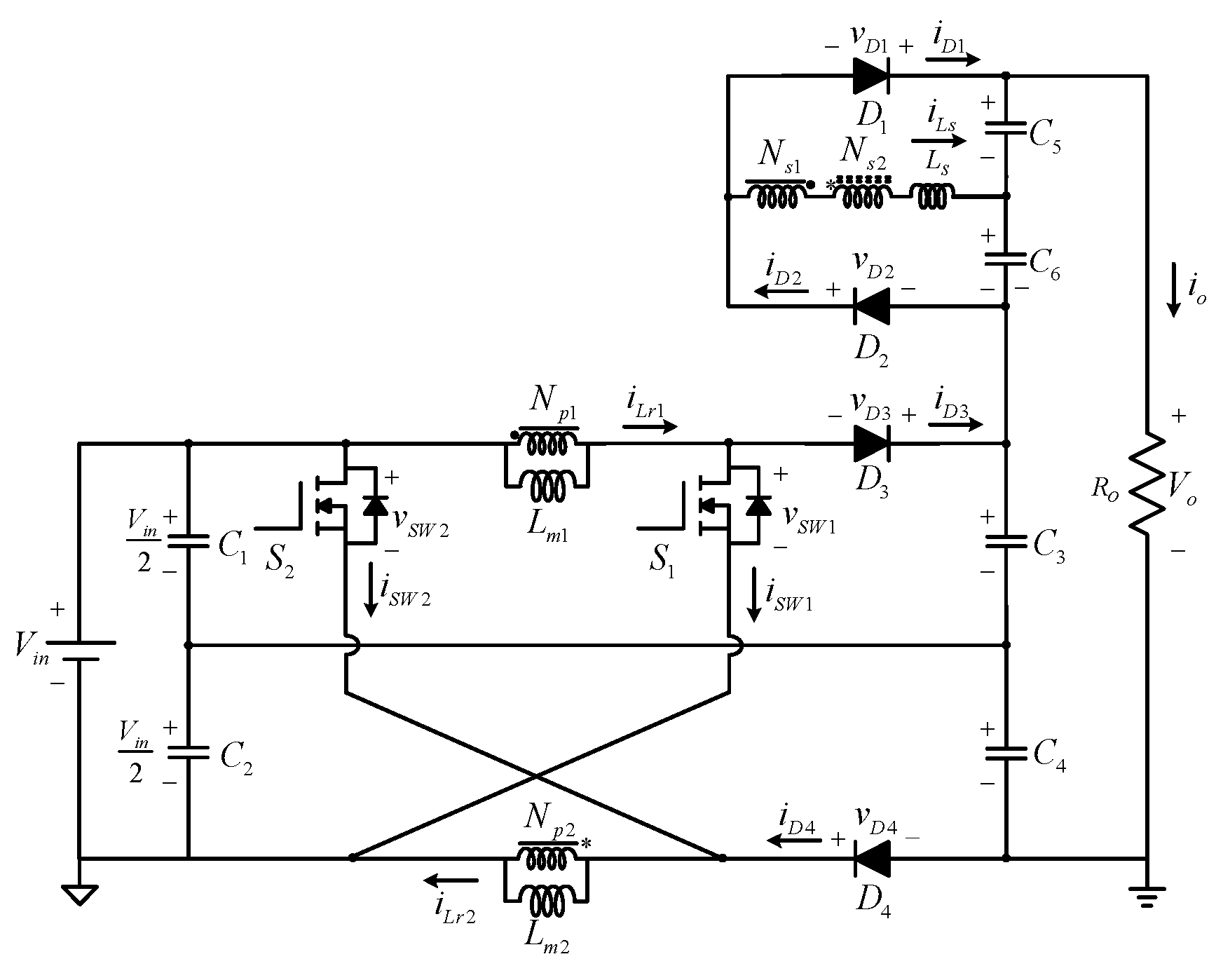
23] can also be used to achieve much higher voltage gain and decrease the voltage stresses of the switches and diodes in the proposed active-switched coupled-inductor high-step-up DC/DC converter as shown in
Figure 1. On the other hand, the proposed converter operated in interleaved mode can also obtain the lower input current ripple. The advantages of the proposed converters are thus demonstrated as follows.
- (1)
Simple and innovative topology: The symmetrical circuit structure is simple and the components are few. The new active-switched coupled-inductor boost technology features both switching inductor and coupled inductor boost characteristics so the converter can be easier to achieve a higher voltage gain.
- (2)
High voltage gain: The converter has a high boost voltage conversion ratio without an extremely large duty cycle and the turns ratio is used to allows a high voltage gain and much freedom of design.
- (3)
High-power applications: For renewable energy power generation systems, the input voltage is usually low so there is a large input current for the high-power applications. The symmetric structure of the proposed converter using an interleaved operation can share the large input current and reduce input current ripple, simultaneously. This paper proposes a converter with an output power of 1 kW.
- (4)
Low voltage stress: For a specific power application, due to the symmetrical circuit structure and the active-switched coupled-inductor high-step-up technique for the proposed converter, the voltage stress on the switches is much less than the output voltage of 400 V.
- (5)
High efficiency: The interleaved operation and symmetrical structure reduces the voltage and current stress on the switches and diodes, so switches with low ON-resistance and diodes with low forward voltage are used to reduce conduction losses and increase overall efficiency. The maximum efficiency for the converter is 95.5%.
2. Proposed Converter and Operating Principle
The proposed converter is shown in
Figure 1.
and
are power switches,
and
are magnetizing inductors and
,
,
and
are the number of turns in the primary and secondary coils, respectively.
and
are voltage-doubling diodes,
and
are clamping diodes,
and
are input capacitors,
and
are clamping capacitors,
and
are voltage-doubling capacitors,
is the input voltage,
is the output voltage and
is the output load.
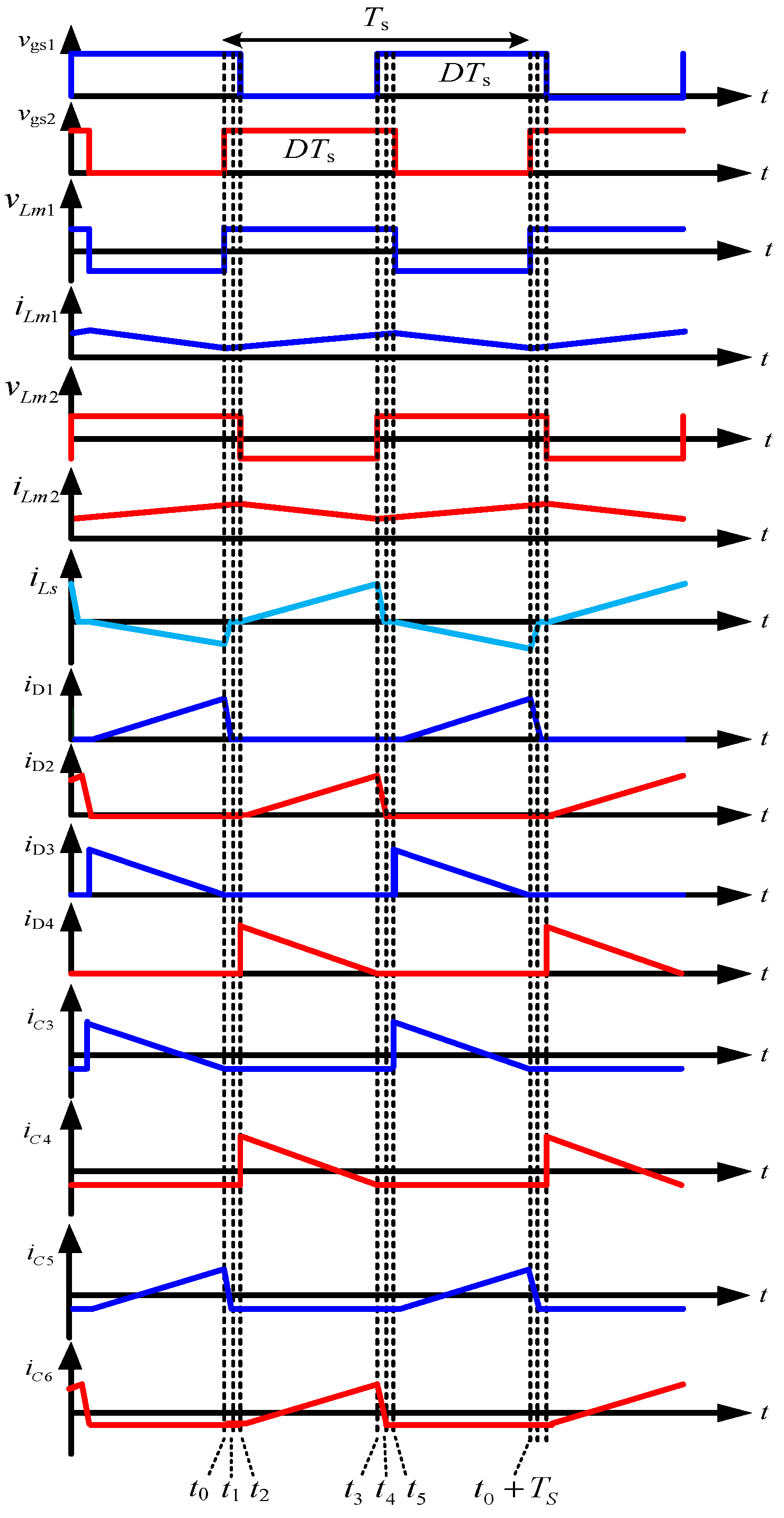
The theoretical key waveforms for proposed converter operating in continuous conduction mode (CCM) are shown in
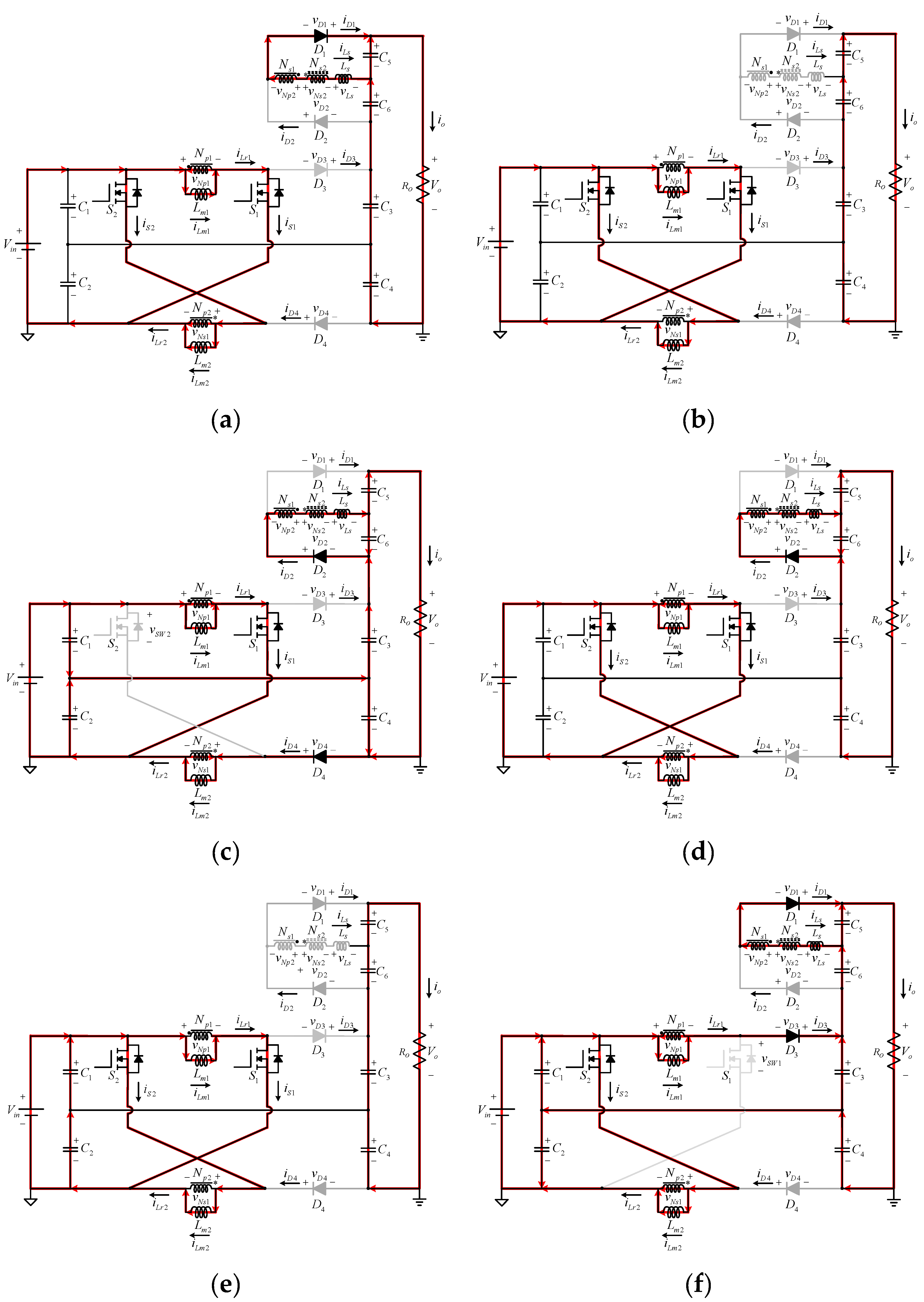
Figure 2. The proposed converter has six linear stages during one switching cycle. The equivalent circuits for these stages are shown in
Figure 3.
The following assumptions are made before the theoretic analyzing.
- (1)
The converter is operating in a steady-state.
- (2)
The magnetizing inductors and are assumed to be sufficiently large to allow the magnetizing inductor current to operate in continuous conduction mode (CCM).
- (3)
Inductors, capacitors, power switches and diodes are ideal.
- (4)
, , , , , and are sufficiently large that the voltage is regarded as constant within one switching cycle.
Stage 1 []: This stage starts at
, when power switches
and
are turned on. Diodes
,
and
are turned off due to the reverse-bias. Diode
remains on due to discharge of the leakage inductor current
. The path for current flow is shown in
Figure 3a. The voltages across the inductors at this stage are:
Inductor currents
,
and
all increase linearly and the reverse-bias for diodes
,
and
is:
As the leakage inductor current increases to zero at , is turned off and the next stage begins.
Stage 2 []: This stage starts at
. Power switches
and
are still on. Diodes
,
,
and
become reverse-bias. The path for current flow is shown in
Figure 3b. The voltages across inductors at this stage are:
Inductor currents
and
both increase linearly and
remains at zero. The voltages across diodes
,
,
, and
are:
If , power switch is turned from on to off and this stage ends.
Stage 3 []: This stage starts at
. Power switch
is turned off, and the power switch
still on. Diodes
and
are still off due to the reverse-bias. The magnetizing inductor current
decreases and inductor
is discharged to the load through
and
so the diodes
and
are forced to conduct. The path for current flow is shown in
Figure 3c. The voltages across the inductors at this stage are:
Inductor currents
and
still increase linearly and
decreases linearly. At this stage, the voltage across power switch
is:
The reverse-bias voltages for diodes
and
are:
At , power switch is turned on again and this stage ends and the next stage begins.
Stage 4 []: This stage starts at
, when power switch
is turned on and power switch
remains on. At this time, diode
is turned off due to the reverse-bias. The path for current flow is shown in
Figure 3d. The voltages across the inductors at this stage are:
Inductor currents
and
increase linearly and
decreases linearly. At this time, the reverse-bias voltages across diodes
,
and
are:
At , the leakage inductor current is reduced to zero so is turned off and the next stage begins.
Stage 5 []: This stage starts at
. Power switches
and
remain on, and diodes
,
and
are off. The path for current flow is shown in
Figure 3e. The operation for this stage is exactly the same as that for Stage 2, so it is not described in detail again at this stage. At
, power switch
is turned off and this stage ends and the next begins.
Stage 6 []: This stage starts at
. Power switch
is turned off, power switch
remains on, and diodes
and
are both off. The magnetizing inductor current
begins to decrease and inductor
is discharged to the load through
and
so diodes
and
are forced to conduct. The path for current flow is shown in
Figure 3f. The voltage across the inductors at this stage is:
Inductor currents
and
decrease linearly and
increases linearly. At this stage, the voltage across power switch
is:
The voltage across diodes
and
is:
When , power switch is turned on again to complete one switching cycle for the circuit.
3. Steady-State Analysis
This section analyzes the converter's voltage gain ratio, component voltage stress and the design conditions for inductors and capacitors in a steady state. At last, the performance comparison with some high step-up converters in literature is also presented herein.
3.1. Voltage Gain Ratio Derivation
Applying the volt–second balance principle to magnetizing inductors
and
, the voltage across capacitors
and
is:
To simplify the analysis, the leakage inductor is ignored for Stages 3 and 6, so the voltage across capacitors
and
is:
Substituting (18) into (19) gives:
By using Equations (18) and (20), the voltage gain ratio for the converter is calculated as:
There are two design conditions that affect the voltage gain for the converter: the coupled turns ratio and the duty cycle . There are two degrees of freedom in the voltage-gain design. Appropriate values for and ensure that there is a high voltage gain without using a extremely duty cycle.
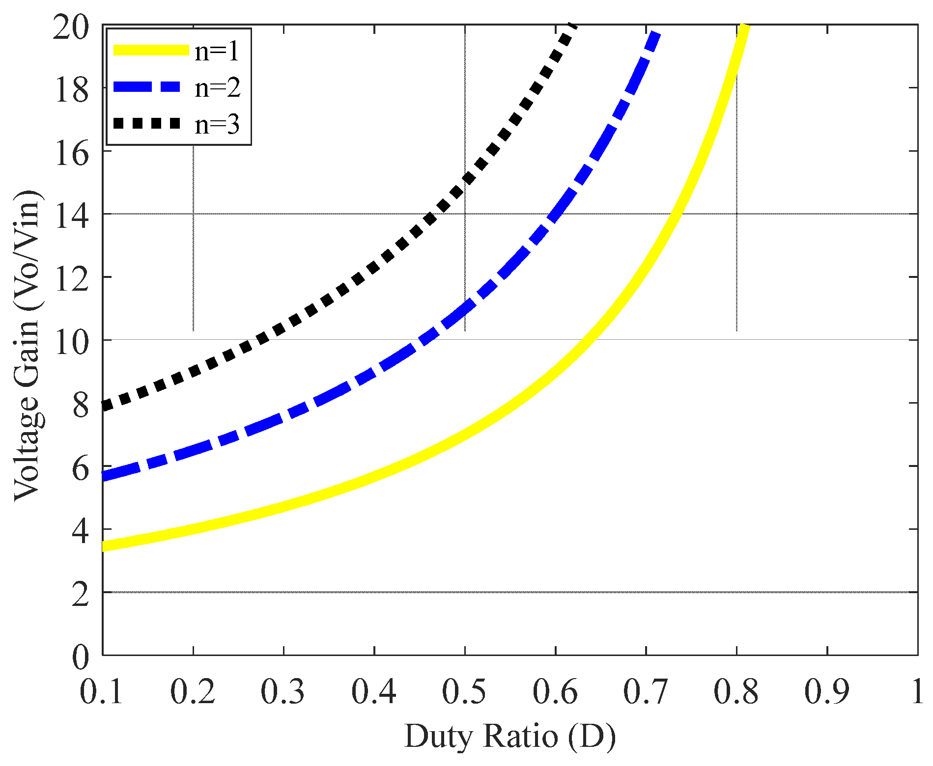
The voltage gain curve for the proposed converter is shown in
Figure 4. If either the duty cycle or the turns ratio is increased, the voltage gain increases. If the turns ratio of the coupled inductor is
, the voltage gain is 10 with
and if the turns ratio for the coupled inductor is
, the voltage gain can achieve 20 with
.
3.2. Voltage Stresses on Semiconductor Devices
When power switches
and
are off, the voltage stresses are calculated as:
When the diodes are off, the voltage stresses are:
3.3. Design of Inductors
Assuming the current sharing is achieved, the currents of magnetizing inductors
and
are the same after one of those currents are shifted half switching period.
is the average current of magnetizing inductors
and
, and
is the inductor ripple current. When the converter operates in CCM. It shows that
The average magnetizing inductor current is half of the average input current. It yields
where
is the average output power. The inductor current ripple
is written as:
Substituting (29)-(30) into (28) gives the design condition for inductor
as:
3.4. Design of Capacitors
Based on the charges for capacitors through the circuit in
Figure 2, it gives:
The capacitances are calculated using Equation (32) as:
Equations (18), (20) and (21) are substituted into this equation (33) to get:
3.5. Performance Comparison
In this paper, a comparison with three high step-up converters [
19,
20,
21] is given. The comparison shown in
Table 1 includes voltage gain, the value of voltage gain at n=1 and D=0.6, voltage stresses of switches and diodes, number of switches, diodes, capacitors, cores and winding, input current sharing ability, and efficiency at 200-250 W. It shows that the proposed converter has the higher voltage gain of 9 than 7 of converter in [
20] and 6.25 of converter in [
21]. In order to obtain the same voltage gain, the converters in [
20] and [
21] are required larger turn ratios or duty cycles, which thereby increase power losses. It also can see that the efficiency 95.5 % of the proposed converter at 200 W is higher than those 94.3 % and 92 % of the converters in [
20] and [
21], respectively. In addition, the proposed converter and the converter in [
20] have the current sharing ability, but the converter in [
21] does not have. It reveals that the current flowing through the components of the converter in [
21] is larger than those of the proposed converter and converter in [
20], so the converter in [
21] has higher conduction losses and worse power efficiency.
On the other hand, by comparing with the proposed converter and the converter in [
19], it gives that they can offer the same high voltage gain but the proposed converter has fewer components, resulting in a smaller volume, higher power density, and fewer magnetic cores, reducing volume and magnetic core losses. Moreover, the proposed converter exhibits lower power switch and diode voltage stresses compared to converters [
19,
20,
21]. Therefore, low conduction resistance switches can be used to reduce conduction losses and costs. This is the reason why the efficiency of the proposed converter is also higher than that of the converter in [
19].
4. Controller Design
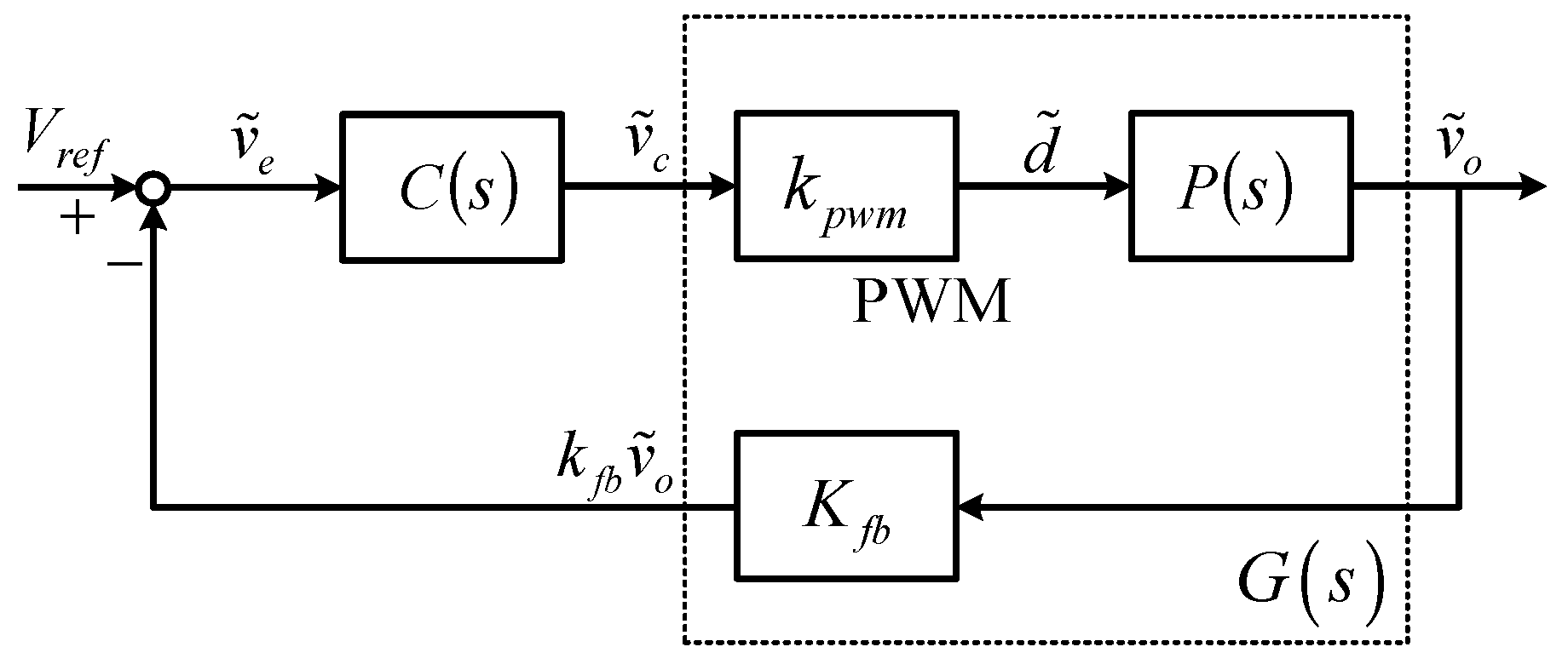
A controller is designed to regulate the output voltage of the proposed converter with variations in input voltage and load. The control block diagram is shown in
Figure 5. T The transfer function
is obtained from the control signal
to the output voltage divider signal
. It is written as:
where the equivalent gain for the PWM (pulse width modulation) circuit is
, the transfer function of proposed converter is
,
is the feedback voltage gain. Moreover,
is a controller that needs to be designed.
A prototype converter was constructed and tested. The specifications of the proposed converter and component parameters derived from the design considerations are shown in
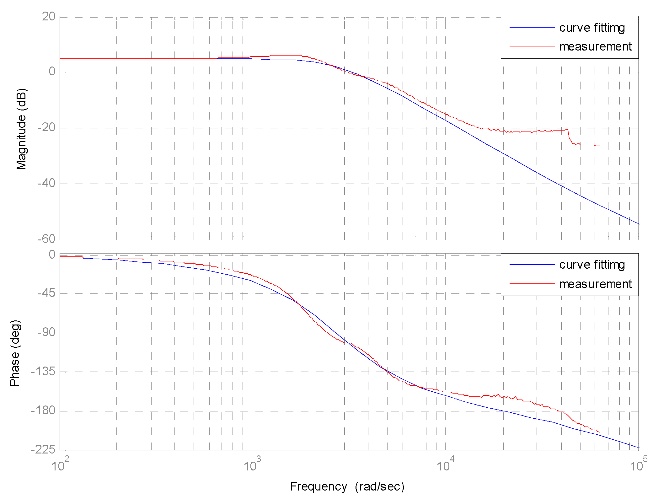
Table 2. A frequency response analyzer (FRA51602) was used to measure the Bode plots of the plant
for an output power of 500 W. The result is shown in
Figure 6. The red curves are the measured results and the blue curves are derived by curve fitting using MATLAB software. It shows that the two curves are similar in terms of gain and phase. Therefore, the small-signal transfer function for the proposed converter is obtained as:
Based on (36), the voltage feedback controller is designed by the K-factor method [
27]. A 45° phase margin at a crossover frequency of 1 kHz is given that a Type III controller is designed as
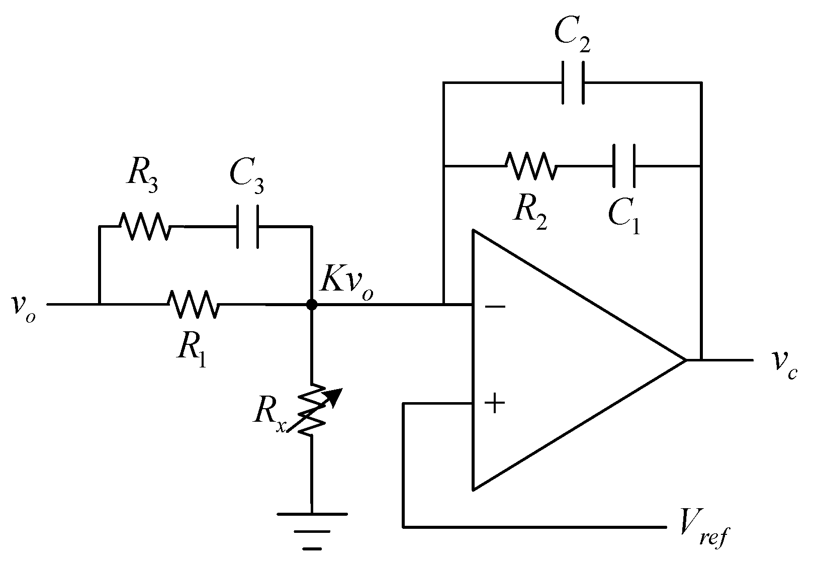
The Type III controller is implemented using an operational amplifier circuit shown in
Figure 7, and the transfer function of the proposed Type-III controller is presented as
From (37) and (38), the passive components of the Type III controller in
Figure 7 can be calculated and used to realize the designed controller, where it yields
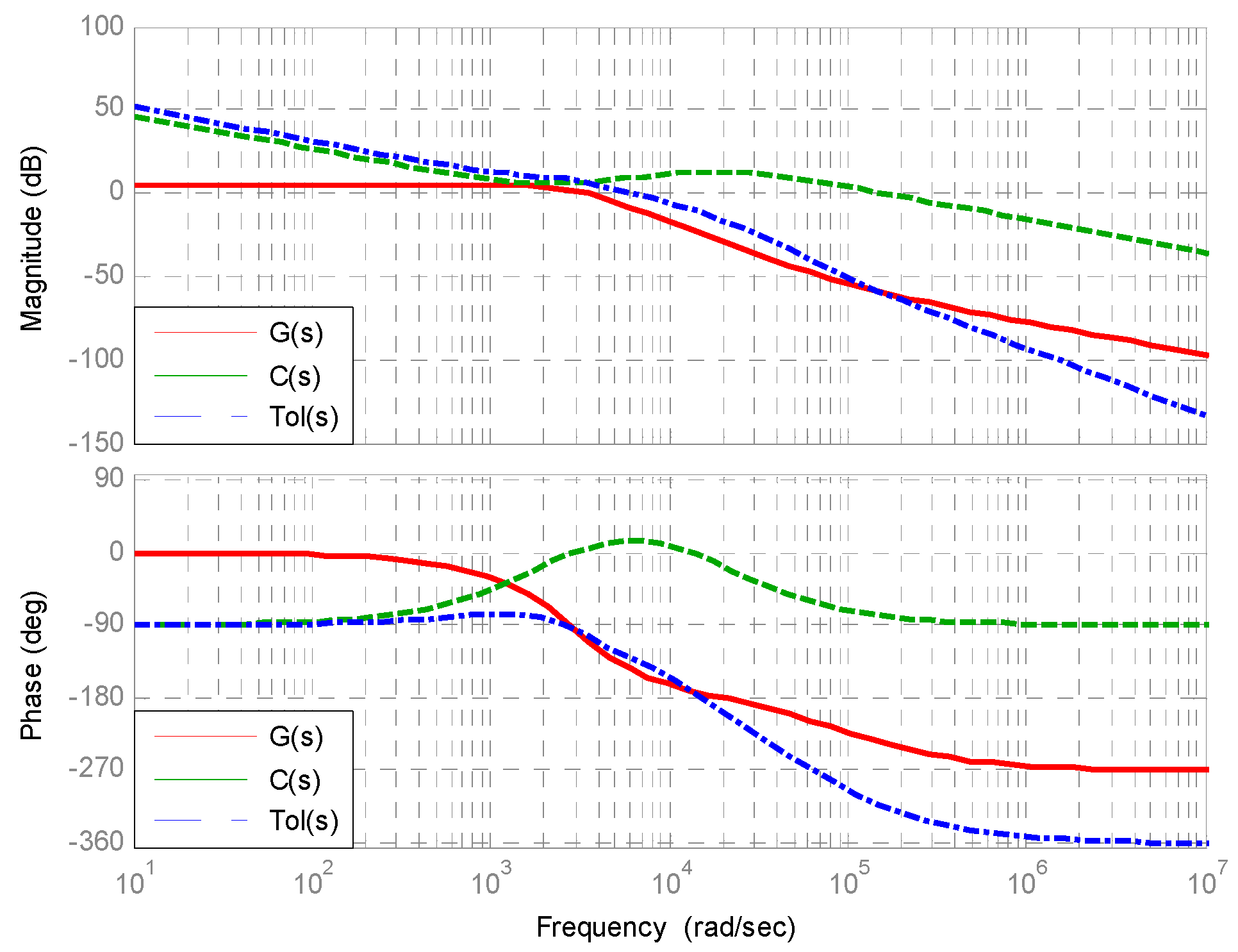
Finally, the Bode plots for plant
, the Bode plots for the controller
and the Bode plots for the open-loop system
can be drawn and shown in
Figure 8. It reveals that a 45° phase margin at a crossover frequency of 1 kHz is achieved.
5. Simulations and Experimental Results
This paper simulates and implements a proposed converter operating at 200-1000 W.
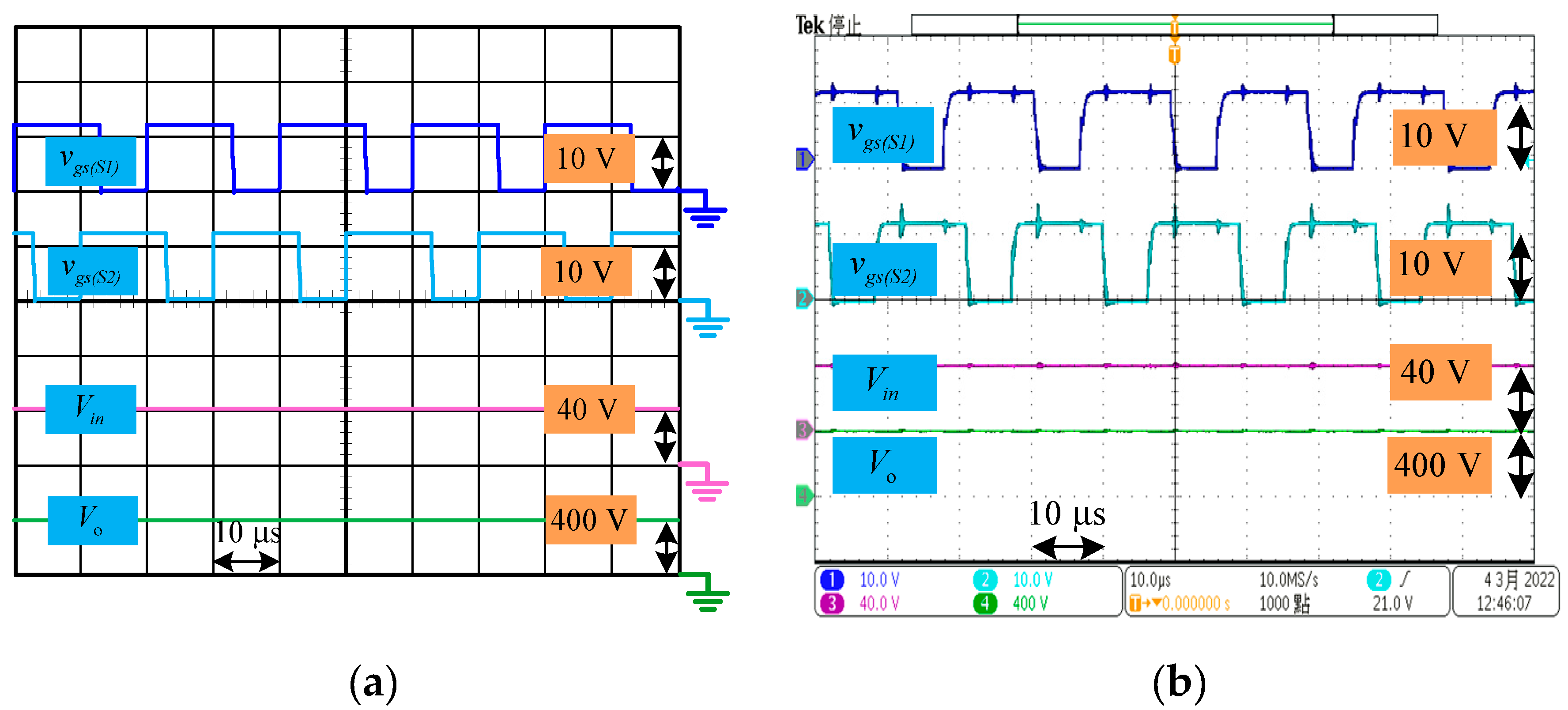
Figure 9,
Figure 10,
Figure 11,
Figure 12 and
Figure 13 show the waveforms for the Is-Spice simulations and experimental results for the proposed converter at 1 kW in the steady state.
Figure 9 shows that the input voltage
is 40 V and the output voltage
is 400 V. The high voltage gain of 10 is achieved herein. From the drive signals for the switches, it shows that the duty cycle for simulation is 0.643, for experimental result is 0.67. The duty cycle for theoretical value is 0.636 calculated form (21). There is a significant reduction in voltage drop in practice because the actual components are not ideal, so the duty cycle for experimental result is slightly higher than those for simulation and the theoretical result.
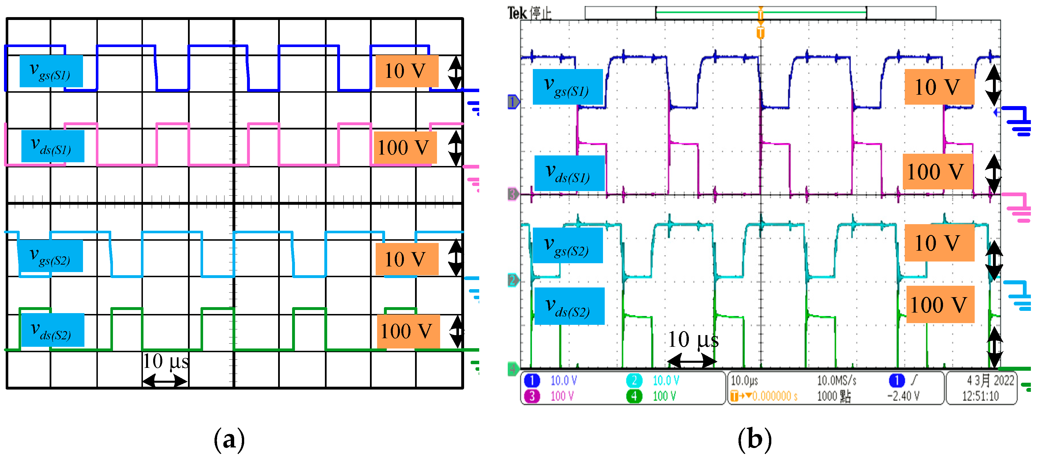
The waveforms for voltages
and
across power switches
and
are shown in
Figure 10. The simulations and experimental results of voltage stresses
and
in steady state are 114 V and 112 V, respectively. Both of them are close to the theoretical results of 110 V. Therefore, the switches for the proposed converter have low voltage stress.
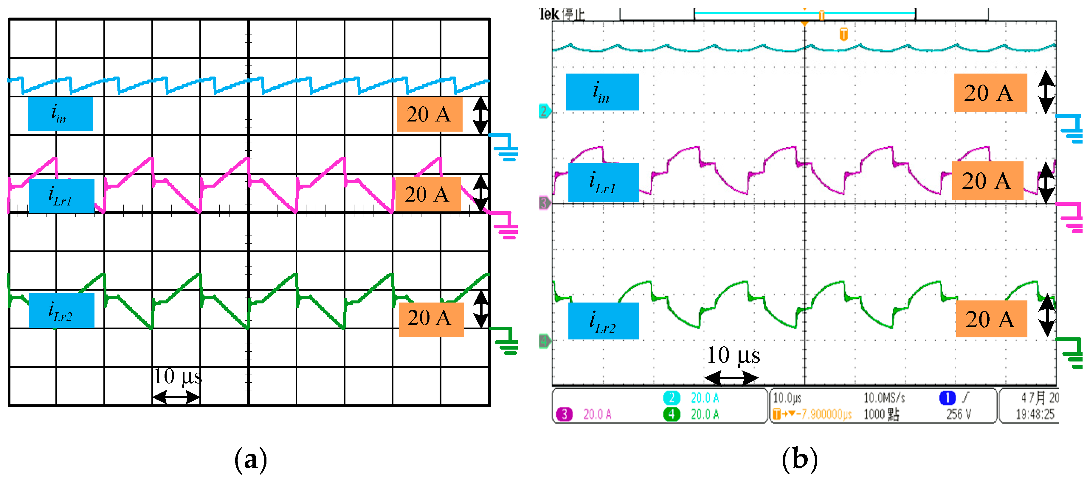
The converter is a symmetrical structure and current
is similar to
but interleaved with a
phase shift. The waveforms for input current
, currents
and
are shown in
Figure 11. The average currents of
and
are the same of 14.2 A for the simulation results and are 14.42 A and 14.52 A respectively for the experiment results. Therefore, the converter features the performance of current sharing. Moreover, it reveals from
Figure 11 that the current ripples of the input current
are 7.74 A and 3.95 A for simulation and experimental result respectively. They become much smaller than the current ripples of
and
, which are 27.8 A and 21.4 A for simulation and experimental result respectively.
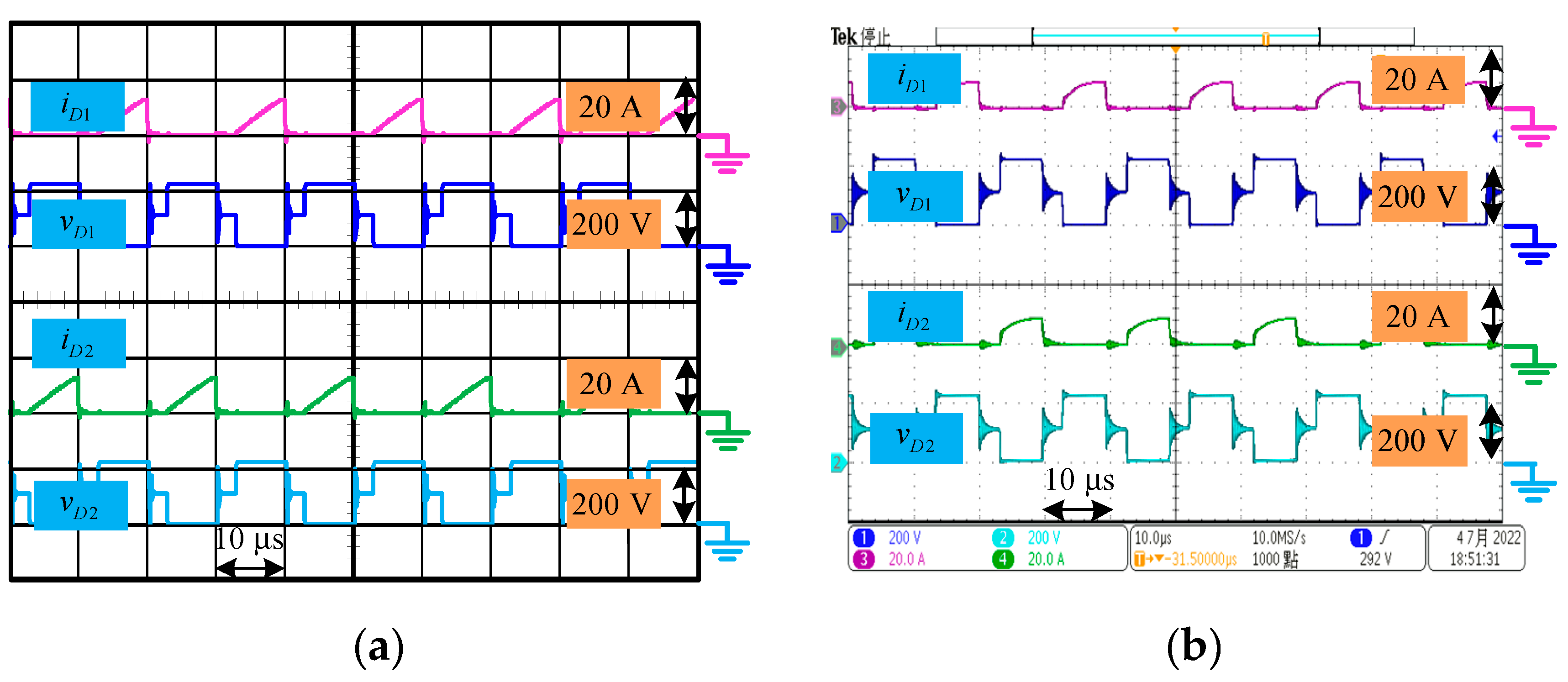
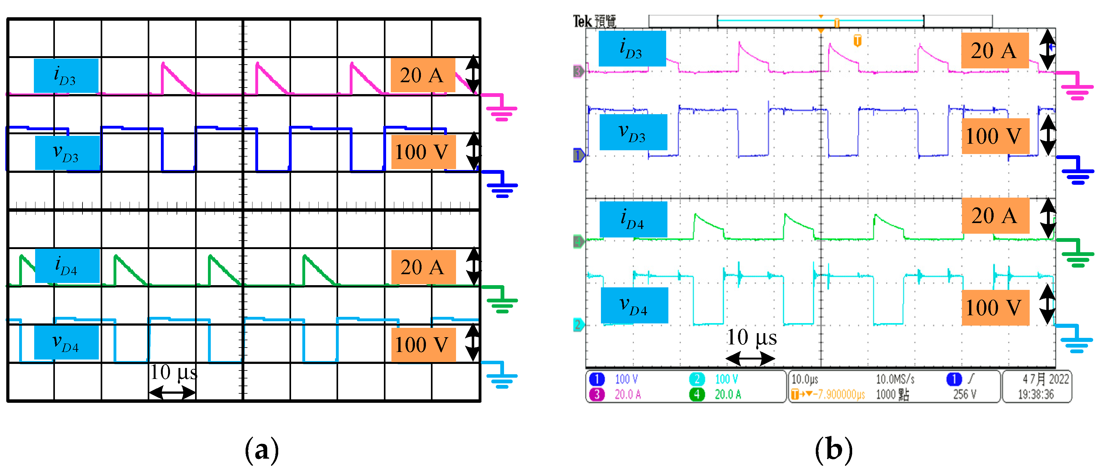
The current and voltage waveforms for diodes
and
are shown in
Figure 12. The current and voltage waveforms for diodes
and
are shown in
Figure 13. It shows that there is no reverse-recovery problem for all the diodes as diode is turned from on to off. Moreover, it also gives that the maximum voltages across diodes
,
are 220 V, which is about
/2 , and the maximum voltages across diodes
and
are 110 V, which is about
/4 . It means that all of the diodes
, ,
and
have low voltage stress.
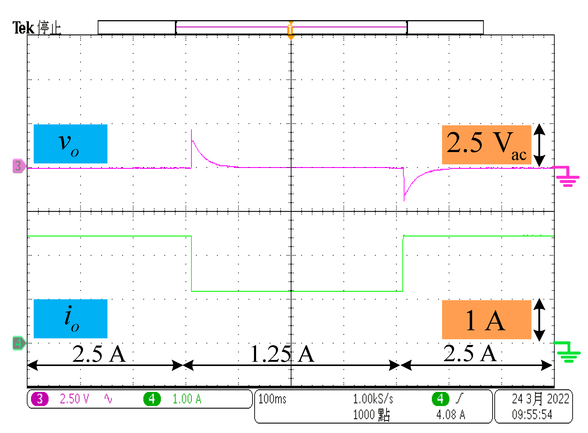
Figure 14 shows the dynamic response for the output voltage when there is a step change in the output load from
to
and then to
. It has a voltage overshoot of 2.3 V, which is much less than the output voltage of 400 V.
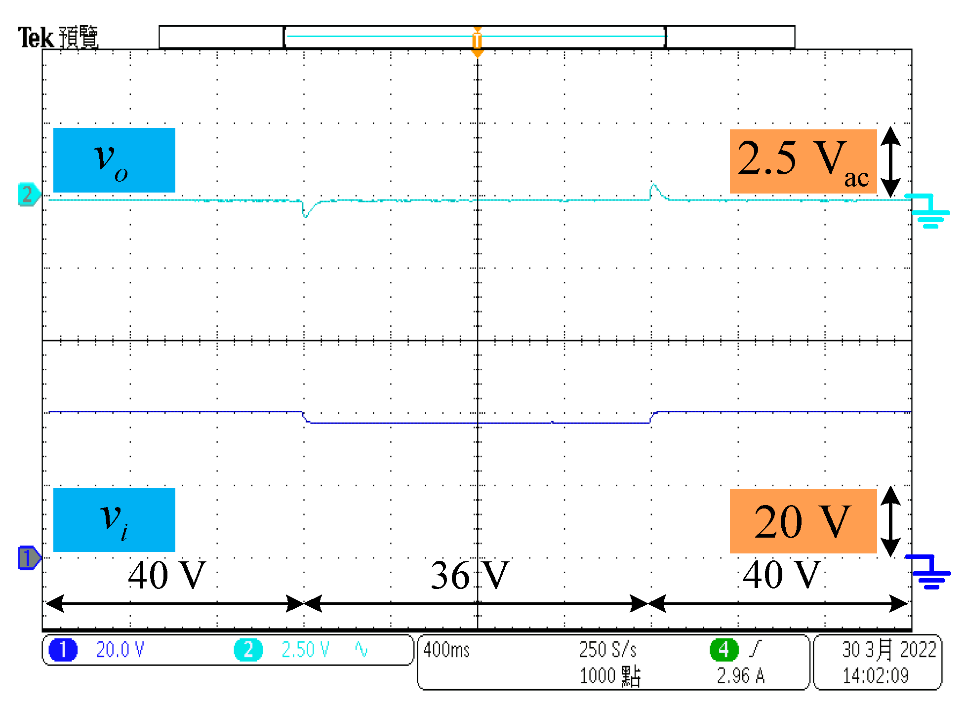
Figure 15 shows the dynamic response for the output voltage when there is a step change in the input voltage from 40 V to 36 V and then to 40 V. The output voltage overshoot is 0.71 V, which is quite smaller than the output voltage of 400 V. The results in these two figures show that the output voltage can be regulated under input voltage and output load variations. It means that the overall system is very robust.
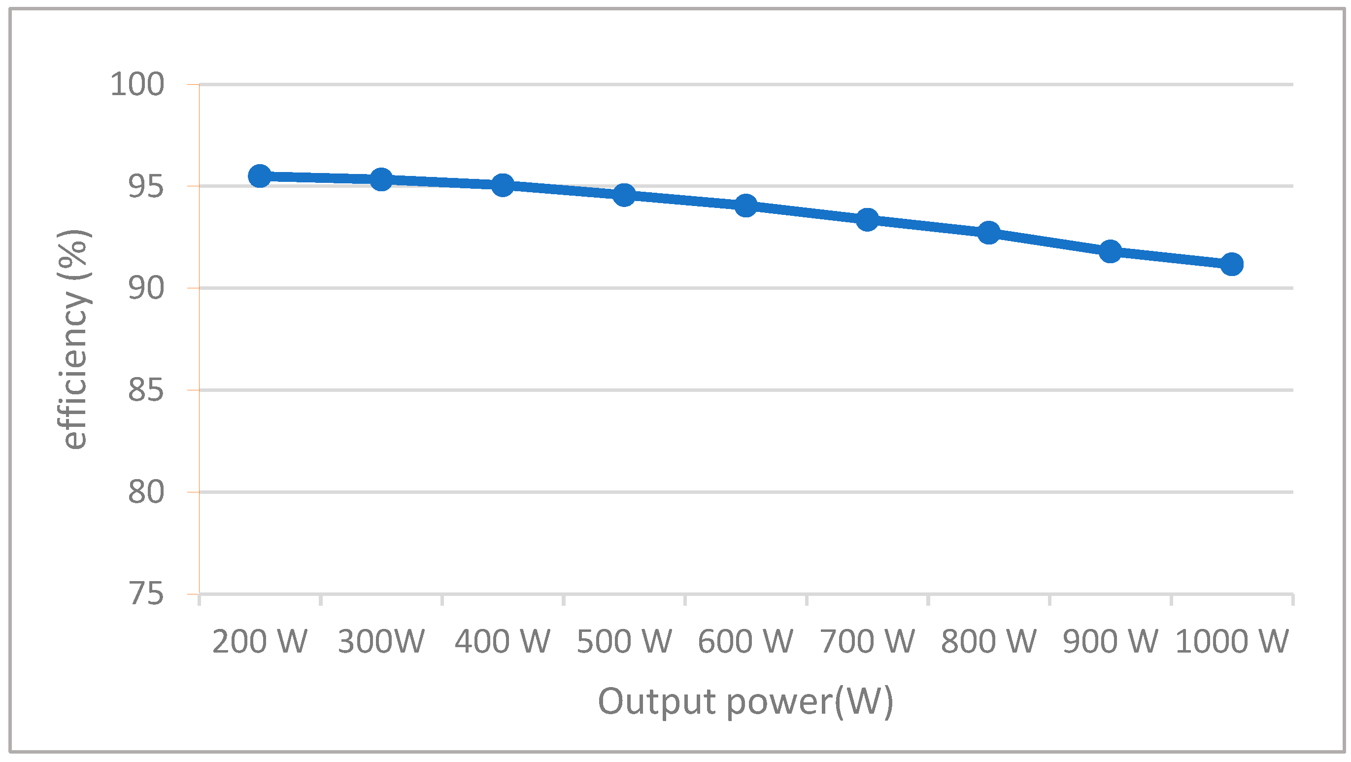
In this paper, the conversion efficiency of the proposed converter for output powers from 200 W to 1000 W was measured by a HIOKI 3390 and the results are shown in
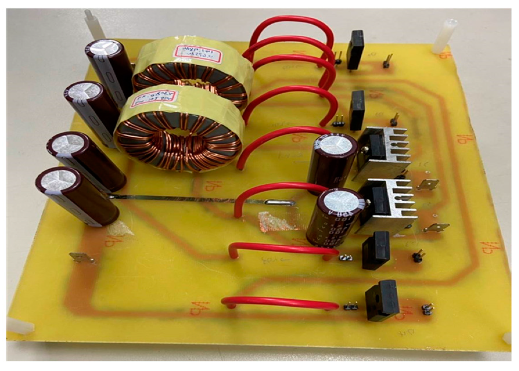
Figure 16. The converter has a maximum efficiency of 95.5 % at a light load of 200 W. A heavy load of 1000 W results in the efficiency of 91.16 %, which is still more than 90 %. Moreover, the picture of the experimental prototype for power stage is also presented in
Figure 17. It shows that the proposed converter has a simple circuit structure with fewer components.
6. Conclusion
This paper proposes a novel symmetrical active-switched coupled-inductor high-step-up DC/DC converter. The new active-switched coupled-inductor boost technology features both switching inductor and coupled inductor boost characteristics so the converter can be easier to achieve a higher voltage gain with two design freedom of the turn ratio and the duty cycle and operated without a large duty cycle. Moreover, the voltage stresses on the switches and diodes in the converter are much lower than the output voltage. It gives that the power switches with a smaller ON-resistance and diodes with smaller forward voltage can applied to reduce conduction losses. So the overall efficiency of the proposed converter can be further increased. A steady-state analysis, component design considerations, dynamics and controller design are also presented herein. Finally, a 200-1000 W with 40 V input and 400 V output at 50 kHz switching frequency prototype is implemented. The simulations and experimental results are thereby given to validate the theoretic results. It reveals that the proposed converter exhibits a high voltage gain of 10, low voltage stresses of power switches and diodes, output voltage regulation despite of input voltage and output load variations, and high efficiency of 95.5 % at 200 W. As a result, the proposed converter with high voltage gain, low voltage stress, high efficiency and simple circuit topology can be used for a rectifier giving a 400 V dc bus in a renewable energy generation system.
References
- Tofoli, F.L.; Pereira, D.d.C.; Josias de Paula, W.; Oliveira Junior, D.d.S. Survey on non-isolated high-voltage step-up dc–dc topologies based on the boost converter. IET Power Electronics. 2015, 8, 2044–2057. [Google Scholar] [CrossRef]
- Zhu, B.; Ding, F.; Vilathgamuwa, D.M. Coat Circuits for DC–DC Converters to Improve Voltage Conversion Ratio. IEEE Trans Power Electronics. 2020, 35, 3679–3687. [Google Scholar] [CrossRef]
- Alzahrani, A.; Ferdowsi, M.; Shamsi, P. High-voltage-gain dc-dc step-up converter with bifold dickson voltage multiplier Cells. IEEE Trans Power Electronics. 2019, 34, 9732–9742. [Google Scholar] [CrossRef]
- Ye, Y.; Peng, W.; Jiang, B. High step-up dc-dc converter with multi-winding CL and switched capacitor. IET Power Electronics. 2018, 11, 2232–2240. [Google Scholar] [CrossRef]
- Zhao, J.; Chen, D. Switched-Capacitor High Voltage Gain Z-Source Converter with Common Ground and Reduced Passive Component. IEEE Access. 2021, 9, 21395–21407. [Google Scholar] [CrossRef]
- Lei, H.; Hao, R.; You, X.; Li, F. Nonisolated High Step-Up Soft-Switching DC–DC Converter with Interleaving and Dickson Switched-Capacitor Techniques. IEEE Journal of Emerging and Selected Topics in Power Electronics 2019, 8, 2007–2021. [Google Scholar] [CrossRef]
- Zeng, T.; Wu, Z.; He, L. An interleaved soft switching high step-up converter with low input current ripple and high efficiency. IEEE Access. 2019, 7, 93580–93593. [Google Scholar] [CrossRef]
- Akhlaghi, B.; Molavi, N.; Fekri, M.; Farzanehfard, H. High Step-Up Interleaved ZVT Converter with Low Voltage Stress and Automatic Current Sharing. IEEE Trans Industrial Electronics. 2018, 65, 291–299. [Google Scholar] [CrossRef]
- Axelrod, B.; Beck, Y.; Berkovich, Y. High step-up DC-DC converter based on the switched-coupled-inductor boost converter and diode-capacitor multiplier: steady state and dynamics. IET Power Electronics. 2015, 8, 1420–1428. [Google Scholar] [CrossRef]
- Moradpour, R.; Ardi, H.; Tavakoli, A. Design and Implementation of a New SEPIC-Based High Step-Up DC/DC Converter for Renewable Energy Applications. IEEE Trans on Industrial Electronics. 2018, 65, 1290–1297. [Google Scholar] [CrossRef]
- Luo, P.; Liang, T.J.; Chen, K.H.; Chen, S.M. Design and Implementation of a High Step-Up DC-DC Converter with Active Switched Inductor and Coupled Inductor. In Proceedings of the 2022 International Power Electronics Conference (IPEC-Himeji 2022- ECCE Asia), Himeji, Japan, 15–19 May 2022; pp. 1670–1676. [Google Scholar]
- Tseng, K.C.; Cheng, C.A.; Chen, C.T. High Step-Up Interleaved Boost Converter for Distributed Generation Using Renewable and Alternative Power Sources. IEEE Journal Emerging and Selected Topics in Power Electronics. 2017, 5, 713–722. [Google Scholar] [CrossRef]
- Ardi, H.; Ajami, A. Study on a High Voltage Gain SEPIC-Based DC-DC Converter with Continuous Input Current for Sustainable Energy Applications. IEEE Tran Power Electronics, 2018, 33, 10403–10409. [Google Scholar] [CrossRef]
- Molavi, N.; Adib, E.; Farzanehfard, H. Soft-switching bidirectional DC–DC converter with high voltage conversion ratio. IET Power Electronics. 2018, 11, 33–42. [Google Scholar] [CrossRef]
- Ajami, A.; Ardi, H.; Farakhor, A. A novel high step-up DC/DC converter based on integrating coupled inductor and switched-capacitor techniques for renewable energy applications. IEEE Trans Power Electronics. 2015, 30, 4255–4263. [Google Scholar] [CrossRef]
- Seo, S.W.; Ryu, J.H.; Kim, Y.; Choi, H.H. Non-Isolated High Step-Up DC/DC Converter with Coupled Inductor and Switched Capacitor. IEEE Access. 2022, 8, 217108–217122. [Google Scholar] [CrossRef]
- Seo, S.W.; Ryu, J.H.; Kim, Y.; Lee, J.B. Ultra-High Step-Up Interleaved Converter with Low Voltage Stress. IEEE Access. 2021, 9, 37167–37178. [Google Scholar] [CrossRef]
- Luo, P.; Liang, T.J.; Chen, K.H.; Chen, S.M. High Step-up DC-DC Converter with Active Switched Inductor and Voltage Double Based on Three-winding Coupled Inductor. In Proceedings of the 2022 IEEE Applied Power Electronics Conference and Exposition(APEC), Houston, TX, USA, 20–24 March 2022; pp. 1–6. [Google Scholar]
- Guepfrih, M.F.; Waltrich, G.; Lazzarin, T.B. High Step-Up DC-DC Converter Using Built-In Transformer Voltage Multiplier Cell and Dual Boost Concepts. IEEE Journal of Emerging and Selected Topics in Power Electronics. 2021, 9, 6700–6712. [Google Scholar] [CrossRef]
- Vaghela, M.A.; Mulla, M.A. High Step-Up Gain Converter Based on Two-Phase Interleaved Coupled Inductor Without Right-Hand Plane Zero. IEEE Transactions on Power Electronics. 2023, 38, 5911–5927. [Google Scholar] [CrossRef]
- Lopez-Santos, O.; Mayo-Maldonado, J.C.; Rosas-Caro, J.C.; Valdez-Resendiz, J.E.; Zambrano-Prada, D.A. Ruiz-Martinez, O.F. Quadratic boost converter with low-output-voltage ripple. IET Power Electronics. 2020, 13, 1605–1612. [Google Scholar] [CrossRef]
- Li, F.; Yao, Y.; Wang, Z.; Liu, H. Coupled-inductor-inverse high step-up converter. IET Power Electronics. 2018, 11, 902–911. [Google Scholar] [CrossRef]
- Henn, G.A.L.; Silva, R.N.A.L.; Praca, P.P.; Barreto, L.H.S.C.; Oliveira, D.S. Interleaved-Boost Converter with High Voltage Gain. IEEE Trans power electronics. 2010, 25, 2753–2761. [Google Scholar] [CrossRef]
- Alateeq, A.; Almalaq, Y.; Matin, M. A Switched-Inductor Model for a Non-Isolated Multilevel Boost Converter. In Proceedings of the 2017 North American Power Symposium (NAPS), Morgantown, WV, USA, 17–19 September 2017; pp. 1–5. [Google Scholar]
- Jose, M.P.; Paulose, S.; John, N.; Paul, B.; Eldo, H.S. CD-Cell Switched Inductor Based Fifth Order Boost Converter. In Proceedings of the 2021 International Conference on Communication, Control and Information Sciences (ICCISc), Idukki, India, 16–18 June 2021; pp. 1–5. [Google Scholar]
- Tang, Y.; Tong, H.; Kan, J.; Zhang, Y.; Xu, K. Symmetric Dual-Switch Converter. IEEE Transactions on Power Electronics. 2020, 35, 11955–11964. [Google Scholar] [CrossRef]
- Venable, D. The K factor: a new mathematical tool for stability analysis and synthesis. Proceedings Powercon 1983, 10. [Google Scholar]
Figure 1.
Proposed converter
Figure 1.
Proposed converter
Figure 2.
Theoretical key waveform for the proposed converter operating in CCM
Figure 2.
Theoretical key waveform for the proposed converter operating in CCM
Figure 3.
Equivalent circuits for: (a) Stage 1, (b) Stage 2, (c) Stage 3, (d) Stage 4, (e) Stage 5 and (f) Stage 6.
Figure 3.
Equivalent circuits for: (a) Stage 1, (b) Stage 2, (c) Stage 3, (d) Stage 4, (e) Stage 5 and (f) Stage 6.
Figure 4.
Voltage gain for the proposed converter versus turns ratio and duty cycle .
Figure 4.
Voltage gain for the proposed converter versus turns ratio and duty cycle .
Figure 5.
Control block diagram for the overall system.
Figure 5.
Control block diagram for the overall system.
Figure 6.
Bode plots for the measurement result (red) and curve fitting result (blue).
Figure 6.
Bode plots for the measurement result (red) and curve fitting result (blue).
Figure 7.
Type III Controller circuit.
Figure 7.
Type III Controller circuit.
Figure 8.
Bode plots for the plant, controller and open-loop system.
Figure 8.
Bode plots for the plant, controller and open-loop system.
Figure 9.
Waveforms for , , and : (a) Simulation results. (b) Experimental results.
Figure 9.
Waveforms for , , and : (a) Simulation results. (b) Experimental results.
Figure 10.
Waveforms for , , and : (a) Simulation results. (b) Experimental results.
Figure 10.
Waveforms for , , and : (a) Simulation results. (b) Experimental results.
Figure 11.
Waveforms for , and : (a) Simulation results. (b) Experimental results.
Figure 11.
Waveforms for , and : (a) Simulation results. (b) Experimental results.
Figure 12.
Waveforms for , , and : (a) Simulation results. (b) Experimental results.
Figure 12.
Waveforms for , , and : (a) Simulation results. (b) Experimental results.
Figure 13.
Waveforms for , , and .: (a) Simulation results (b) Experimental results.
Figure 13.
Waveforms for , , and .: (a) Simulation results (b) Experimental results.
Figure 14.
Dynamic response for output voltage for a step change in load ().
Figure 14.
Dynamic response for output voltage for a step change in load ().
Figure 15.
Dynamic response for output voltage for a change in input voltage ().
Figure 15.
Dynamic response for output voltage for a change in input voltage ().
Figure 16.
Measured efficiency of the proposed converter.
Figure 16.
Measured efficiency of the proposed converter.
Figure 17.
Experimental prototype for power stage.
Figure 17.
Experimental prototype for power stage.
Table 1.
Comparison of the proposed converter with other previously presented converters.
Table 1.
Comparison of the proposed converter with other previously presented converters.
| Parameter |
[19] |
[20] |
[21] |
Proposed converter |
| Voltage gain(M) |
|
|
|
|
|
M for n=1, D=0.6 |
9 |
7 |
6.25 |
9 |
Voltage stress
of switch (VS/Vin) |
|
|
|
|
Maximum voltage
stress of diodes (VD/Vin) |
|
|
|
|
Number of elements
Switches/diodes/
capacitors/cores/
winding |
2/4/6/4/4 |
2/4/3/2/4 |
2/2/2/2/2 |
2/4/6/2/4 |
| Input current sharing |
Yes |
Yes |
No |
Yes |
| Efficiency |
93.2% @200 W |
94.3% @200 W |
92% @250 W |
95.5% @200 W |
Table 2.
Specifications and parameters for the proposed converter.
Table 2.
Specifications and parameters for the proposed converter.
| Parameter/Description |
Specification/Value |
| Input voltage Vin
|
40 V |
| Output voltage Vo
|
400 V |
| Rated output power Po
|
1000 W |
| Switching frequency fs
|
50 kHz |
| Magnetizing inductance Lm
|
140 µH |
| Turns ratio n
|
1 |
| Power switches S1 and S2
|
NTHL020N090SC1 |
| Diodes D1, D2, D3, D4
|
STTH3003CW |
| Capacitor C1, C2, C3, C4, C5, C6
|
100 µF |
|
Disclaimer/Publisher’s Note: The statements, opinions and data contained in all publications are solely those of the individual author(s) and contributor(s) and not of MDPI and/or the editor(s). MDPI and/or the editor(s) disclaim responsibility for any injury to people or property resulting from any ideas, methods, instructions or products referred to in the content. |
© 2023 by the authors. Licensee MDPI, Basel, Switzerland. This article is an open access article distributed under the terms and conditions of the Creative Commons Attribution (CC BY) license (http://creativecommons.org/licenses/by/4.0/).
