1. Introduction
Integrated sustainable production is of great importance for the development of our society and the preservation of acceptable conditions for safe living. Modern society uses a wide variety of materials and it is important to optimize the methods of their production. It is necessary to strive for closed production cycles, within which production waste can be used either to create new products, or can be recovered for further use.
The development of new communication technologies, in particular 5th generation communication (5G), requires the provision of reliable shielding of various types of equipment in order to level the influence of interference on the operation of devices.
Currently, more and more attention is paid to shielding materials, which have a high shielding efficiency with minimal weight and size parameters and production costs [
1,
2]. Metallic micro- and nanostructures [
3,
4,
5], carbon nanomaterials [
6,
7,
8,
9,
10], MXenes [
11,
12,
13,
14], oxides [
15,
16], conductive polymers [
17] with different morphology and particle size are considered as effective shielding materials. From the types of materials described above, porous films [
18,
19], bulk polymer composites and coatings [
20,
21,
22,
23,
24], aerogels [
25,
26,
27] are fabricated, and they are also applied to fabrics [
28,
29,
30].
Also, modern technology requires transparent shielding materials [
31] for shielding windows, computer displays and other transparent objects. Efficient shielding of transparent objects is a much more difficult task. As a rule, only metal micro and nanostructures have a shielding efficiency of more than 30 dB. Examples include micro and nanomeshes formed using photolithography [
32,
33,
34], imprint lithography [
35], cracked template [
36,
37,
38], and Ag nanowires (Ag NW) films [
39,
40].
For the widespread introduction of 5G technologies, in addition to shielding electromagnetic radiation, a problem is being solved that is related to maintaining the signal at a high level. 5G communication, due to the use of a shorter wavelength part of the spectrum than previous generations of communication systems (3G and 4G), is more prone to propagation losses within urban areas, inside residential and office buildings. Under 5G communication in different countries, frequency bands are allocated in the following ranges:
S (2-4 GHz),
K (18-26.5 GHz),
Ka (26.5-40 GHz) and shorter wave bands. To maintain the signal at the required level, it is planned to equip elements of urban development and interior decoration of residential buildings with additional radio wave reflectors capable of operating in a wide frequency range [
41,
42,
43]. Transparent conductors based on metallic micro and nanostructures seem to be the most promising solution for this application. Based on these considerations, it can be assumed that the need for transparent materials capable of reflecting electromagnetic radiation in the
S, K, Ka ranges with a reflection coefficient of more than 90% (-0.5 dB) will constantly grow.
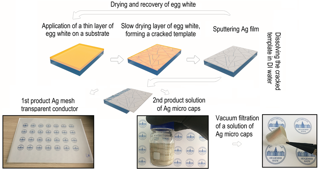
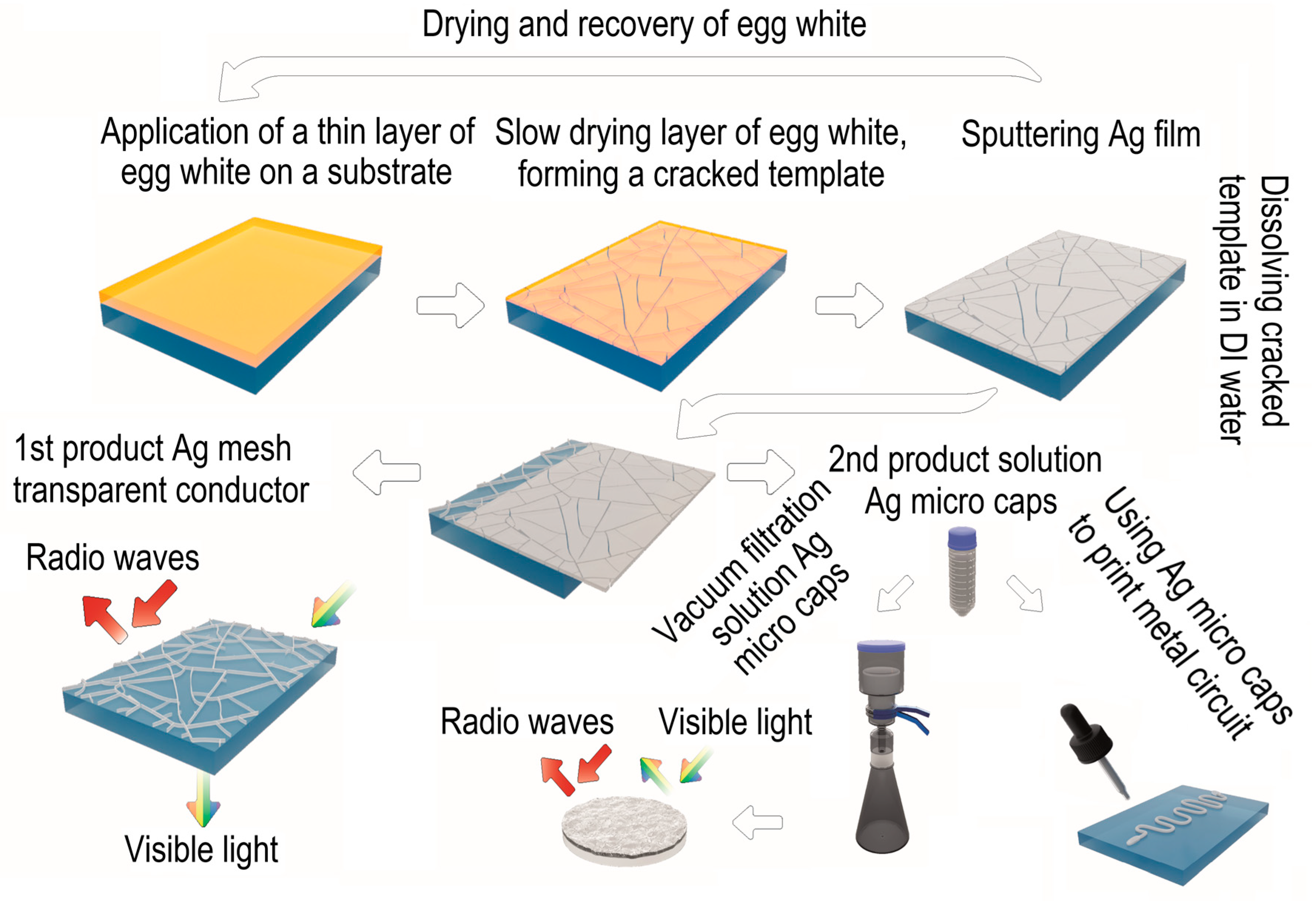
In this paper, we propose an environmentally friendly, technological chain for the production of transparent conductive meshes and micro caps films, which are promising in a number of tasks related to shielding electromagnetic radiation corresponding to 5G communication frequencies. The proposed solution is complex and makes it possible to obtain transparent conductive meshes and micro caps of any chemical composition and strictly specified thickness in a wide range from 10 nm to 1 µm or more. The complete scheme of the technological process is shown in
Figure 1.
In the first step, the egg white is applied to the PET substrate using the Mayer rod method. In the second step, the thin film of egg white is slowly dried at room temperature. During the drying of the egg white film, mechanical stresses build up, as a result of which the film cracks, forming a cracked template. At the third stage, metal is sputtering onto the cracked template. At the fourth stage, the cracked template is dissolved in DI water. After the fourth stage, we have a silver mesh transparent conductor (1st product) and an aqueous solution of silver micro caps and egg white at the output. At the fifth stage, silver micro caps and egg white are separated by decantation (since silver micro caps have a high sedimentation rate). The egg white solution is then dried in order to be recovered and further used to obtain a cracked template. After repeated washing of traces of egg white in DI water, followed by the replacement of the solvent, a solution of silver micro caps (2 nd product) is obtained. Thin porous films or printed tracks for electrical circuits can then be obtained using a solution of silver micro caps.
In this work, silver obtained by magnetron and thermal sputtering methods is considered as model materials. Silver is a model system that exhibits high structural quality and excellent optoelectric performance in both transparent conductive meshes and micro caps.
2. Materials and Methods
2.1. Materials
Egg white and yolk were taken from eggs bought at the food market. Ag (99.99%), targets Kurt J. Lesker (Kurt J. Lesker Company, Jefferson Hills, PA, USA). DI water, isopropyl alcohol. PET film with the thickness 125 µm was bought from HiFi Industrial Film Ltd. (Hi-Fi Industrial Film Ltd., Stevenage, Hertfordshire, UK).
2.2. Preparation of Cracked Template with Peeled Cells Perimeter
Egg white solutions with a yolk concentration of 2 ml/l were deposited by the Meyer rod method on PET substrates. The thickness of the egg white film is 50.48 μm (Meyer rod #12), which was deposited at a speed of 30 mm/s. After deposition, the liquid film was dried at room temperature ~21 °C and a humidity of 50 %.
Then, according to our previous work [
44], we performed two iterations of partial peeling of the cells perimeter of the cracked template. Moisturizing time was 5 sec, shock drying temperature 120 °C.
2.3. Sputtering Silver Films on Cracked Template
To compare the parameters of mesh transparent conductor and silver micro caps, two deposition methods were chosen: magnetron and thermal. Three silver thicknesses of 100, 300, and 600 nm are considered in this work. Magnetron sputtering silver film had the M-100, M-300 and M-600 nomenclature. Thermal sputtering silver film had the T-100, T-300 and T-600 nomenclature.
2.4. Silver Micro Caps Purification, Selective Separation into Flakes and Ribbons
Purification of silver micro caps from traces of egg white was carried out as follows: at the first stage, the egg white was washed by settling in a large volume of distilled water, this operation was repeated five times. After washing out traces of egg white, a solvent replacement operation was performed. Complete replacement of the solvent was carried out by centrifugation. We used isopropyl alcohol as a solvent. For complete replacement, the solution was subjected to centrifugation at a speed of 1000 rpm. This operation was repeated 3 times.
For the selective separation of silver micro caps into silver flakes and silver ribbons, a solution of silver micro caps in isopropyl alcohol was sonicated on a UZTA-0.15/22-O apparatus (U-sonic, Biysk, Russia) for 1 min; the specific power was ~25 W/cm2. After sonication, the separation of silver flakes and silver ribbons was carried out by sedimentation fractionation. The sedimentation time was chosen to be 1, 5, and 15 min.
2.5. Silver Micro Caps Films Preparation
Silver micro caps thin film were formed by vacuum filtration. A PTFE filter (Vladipor, Vladimir, Russia) with an average pore size of 0.2–0.5 µm was used. The film thickness was set by the mass of flakes on the filter.
2.6. SEM, AFM and EDX Analysis of Silver Micro Caps, Silver Flakes and Silver Ribbons
The morphology of silver meshes and silver micro caps was studied by the method of scanning electron microscopy (SEM) using Hitachi TM-4000 Plus (Hitachi, Tokyo, Japan), with the accelerating voltage 5-20 kV. SEM equiped with an energo-dispersive X-Ray spectrometer X-Flash 630Hc (EDX, Bruker, Billerica, MA, USA).
The local surface morphology and thickness of flakes were determined by atomic force microscopy (AFM), DPN 5000 NanoInk (Nanoink Inc., Skokie, IL, USA). For best results, scanning was carried out in semi contact mode using high-resolution cantilevers VIT_P/IR (TipsNano) with a curvature radius of 10 nm. The sample preparation was as follows, on a clean p-Si wafer with (111) orientation, 20 µl of a dilute dispersion of silver micro caps, silver flakes and silver ribbons in isopropyl alcohol was applied. After that, the samples were dried in a muffle furnace at a temperature of 90 °C for 1 hour.
2.7. XRD Analysis of Silver Micro Caps Films
The powder diffraction data of samples for Rietveld analysis were collected at room temperature with a DX-2700BH (Haoyuan Instrument co., Dandong City, Liaoning Province, People’s Republic of China) powder diffractometer with Cu-Kα radiation and linear detector. The step size of 2θ was 0.01°, and the counting time was 0.2 s per step. Rietveld refinement of all structures were performed using TOPAS 4.2.
2.8. Optical Transmittance and Sheet Resistance Measurements of Silver Meshes and Silver Micro Caps Films
The spectral dependencies of the optical transmittance of the meshes were measured in the range of 400–780 nm with a spectrophotometer UV-3600 (Shimadzu, Kyoto, Japan).
A four-probe method was used for sheet resistance measurements using a Keithley 2000 multimeter (Keithley Instruments, Solon, OH, USA) and a four-probe head Mill-Max 854-22-004-10-001101 (Mill-Max Mfg. Corp., Oyster Bay, NY, USA).
2.9. Study EMI Shielding Properties of Silver Meshes and Silver Micro Caps Films
In this study, transmission coefficient T and reflection coefficient R for materials were measured using two waveguide cells designed for different frequency ranges.
- 1)
Special air coaxial cell with a diameter of of 16.00/6.95 mm (type II, 50 Ω, GOST RV 51914-2002). The measurements were carried out in the range of 10 MHz to 7 GHz; this frequency range includes the
L (1-2 GHz),
S (2-4 GHz) and
C (4-8 GHz) bands, the ability to measure at low frequencies with a relatively simple and convenient measurement technique with good quality of results. The measurements were carried out on a Keysight FieldFox N9916A vector network analyzer (Keysight Technologies, Santa Rosa, CA, USA). The dynamic measurement range of the
T is 80 dB and the measurement error is not worse ± 2 dB even on low signal level [
44].
- 2)
The measurement in a higher frequency region was carried out in the
K band (18-26.5 GHz) and
Ka band (26.5-40 GHz). The cross sections of the waveguide cell had a rectangular shape with dimensions of 4.3x10.65 mm for
K band and 3.55x7.1 mm for
Ka band. The test sample is placed in the break of the waveguide transmission line. The measurements were carried out on an R&S ZVA 50 vector network analyzer (Rohde & Schwarz GmbH & Co. KG, Munich, Bavaria, Germany) [
37].
All test benches consisted of test cells and had coaxial cable assemblies, for which we performed a full two-port calibration at the cell inputs.
3. Results and Discussion
3.1.1. Morphology and Geometric Characteristics of the Cracked Template and Silver Meshes
In general, a large number of works of both our group [
45,
46] and other groups [
47,
48,
49,
50] are devoted to the analysis of the metal mesh transparent conductor based cracked template. One of the most important issues is the reproducibility of cracked template parameters (cells size and cracks width).
Figure 2 shows an example of the reproducibility of the geometric parameters of a cracked template.
From images of the cracked template at different sections of the roll (at a distance of 50 cm from each other) obtained in the roll2roll process. It can be seen that they have identical average cell size (the average cell size obtained from 10 secant lines is -78.94 µm (
Figure 2b); 77.58 µm (
Figure 2c) and 76.27 µm (
Figure 2d)), which indicates the reproducibility of this method, which has not yet been demonstrated in the literature.
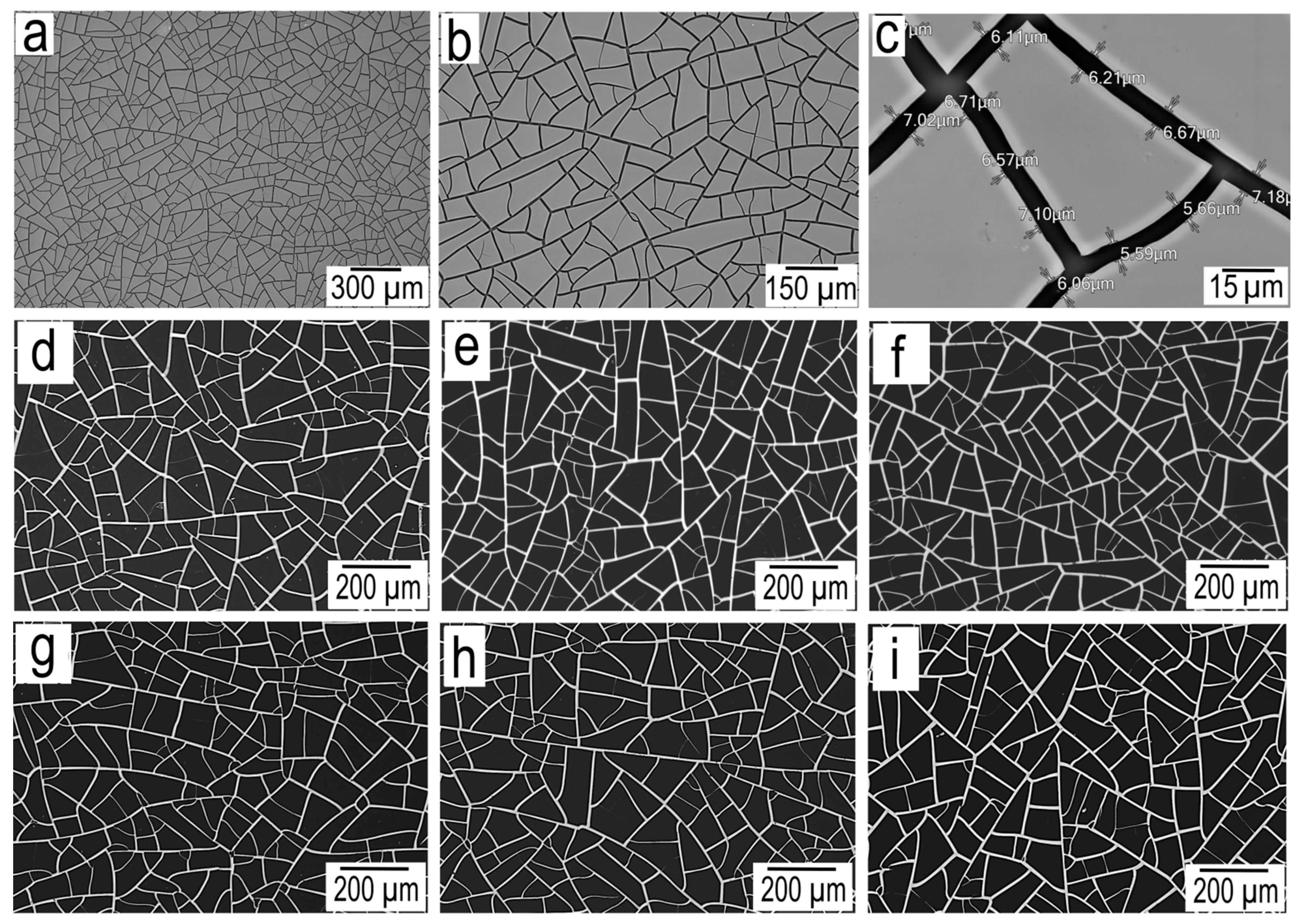
On
Figure 3a-c are
SEM images of the cracked template at various magnifications. We can note the high quality of the cracked template, which is evidenced by the absence of defects that are typical for this type of template. Such defects include missing cells and blind cracks.
SEM images of silver meshes of various thicknesses obtained using magnetron and thermal sputtering are shown in
Figure 3. Morphology analysis shows that all silver meshes have similar geometric parameters. A more detailed analysis of geometric parameters such as average cell size, average fracture width and average
fill factor (FF) is given in
Table 1.
3.1.2. Optoelectric Parameters of Silver Meshes
According to general concepts, the optical transmission of metal micromeshes is proportional to the fill factor. According to [
51], the optical transparency of a mesh transparent conductor can be calculated according to the formula , where
p is the mesh period and
w is the path width. On
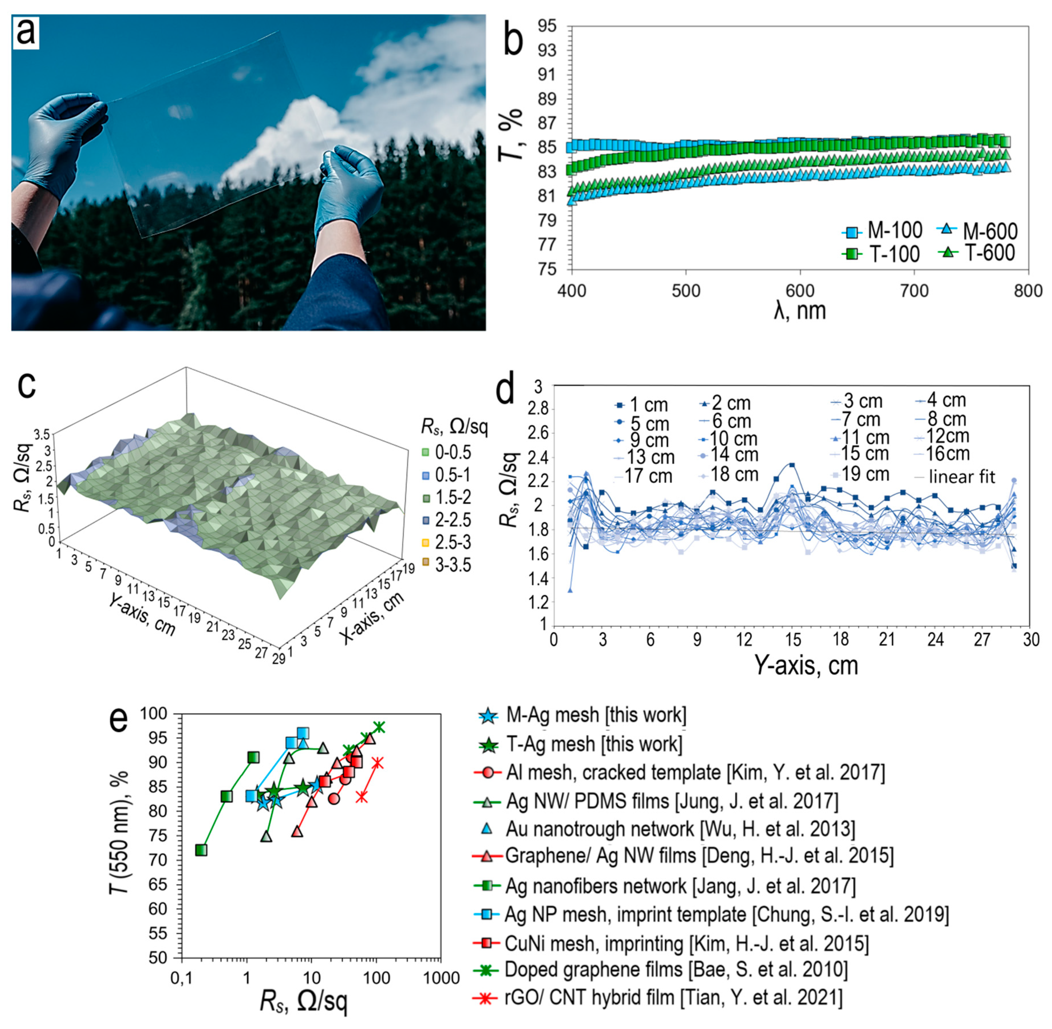
Figure 4a shows the appearance of
T = 1 –
Smesh = (
p −
w)
2/
p2 the T-600 sample, demonstrating its high optical quality and uniformity.
Figure 4b shows the spectral transmission of silver mesh transparent conductor obtained by thermal and magnetron sputtering.
Based on the optical transmission spectra, it can be concluded that an increase in the thickness of the sputtering metal leads to a decrease in transmission, both in the case of magnetron and thermal deposition. Thus, in the case of magnetron sputtering, the transmission of the silver mesh decreases from 85.1 % (M-100) to 82.6 % (M-600) (
Figure 4b). For thermal sputtering, this effect is less pronounced, the transmission decreases from 84.9 % (T-100) to 83.55 % (T-600) (
Figure 4b).
On
Figure 4c shows a 3D plot of sheet resistance versus coordinate for an A4 size silver mesh M-600 sample. Based on the 3D plot analysis, it can be concluded that the sheet resistance is highly uniform over the entire coverage area. The vast majority of points lie in the range of surface resistance 1.5-2 Ω/sq. Only single outliers are observed, lying in the range of 2-2.5 Ω/sq. To determine the average sheet resistance value, a set of sheet resistance graphs was constructed from the Y coordinate along 19 sections with a step of 1 cm. Averaging over all graphs gives the sheet resistance value for silver mesh M-600 equal to 1.84 Ω/sq (
Figure 4d).
Based on the data shown in
Figure 4e, one can judge how the optoelectric parameters of our Ag mesh transparent conductor based cracked template correlate with other popular literature results. In terms of their optoelectric properties, silver meshes are superior to such materials as CNT [
58] and graphene films [
57], Ag NW`s films [
52,
54]. Standing in line with coatings such as Ag NP mesh based on imprint template [
35], Ag nanofibers networks [
55], being at the same time significantly more environmentally friendly and economical in production. It is also worth noting that the cracked template method makes it possible to obtain a significantly thicker silver mesh (h>2µm) [
44]. However, silver micro caps at h>2µm have less potential for practical use. For this reason, in this work, we do not consider materials with a greater thickness of sputtering silver.
3.2.1. Morphology, Structural and Transport Studies Silver Micro Caps and Silver Micro Caps Films
In the literature, as a rule, there are two approaches to obtaining metallic 2D materials, firstly, this is chemical synthesis - solution deposition [
4] or solvothermal synthesis [
59]. Secondly, physical methods, such as wet grinding of spherical particles to give them a flakes shape [
60], repeated folding and calendering binary metal foils [
61], ultrasonic treatment of macroscopic metal foils [
62]. Physical methods also include vacuum deposition of metal on sacrificial polymeric structures [
63]. This method is similar to the results presented by us, however, an important feature of our approach is the fact that in addition to silver micro caps, we obtain high-quality transparent conductive meshes.
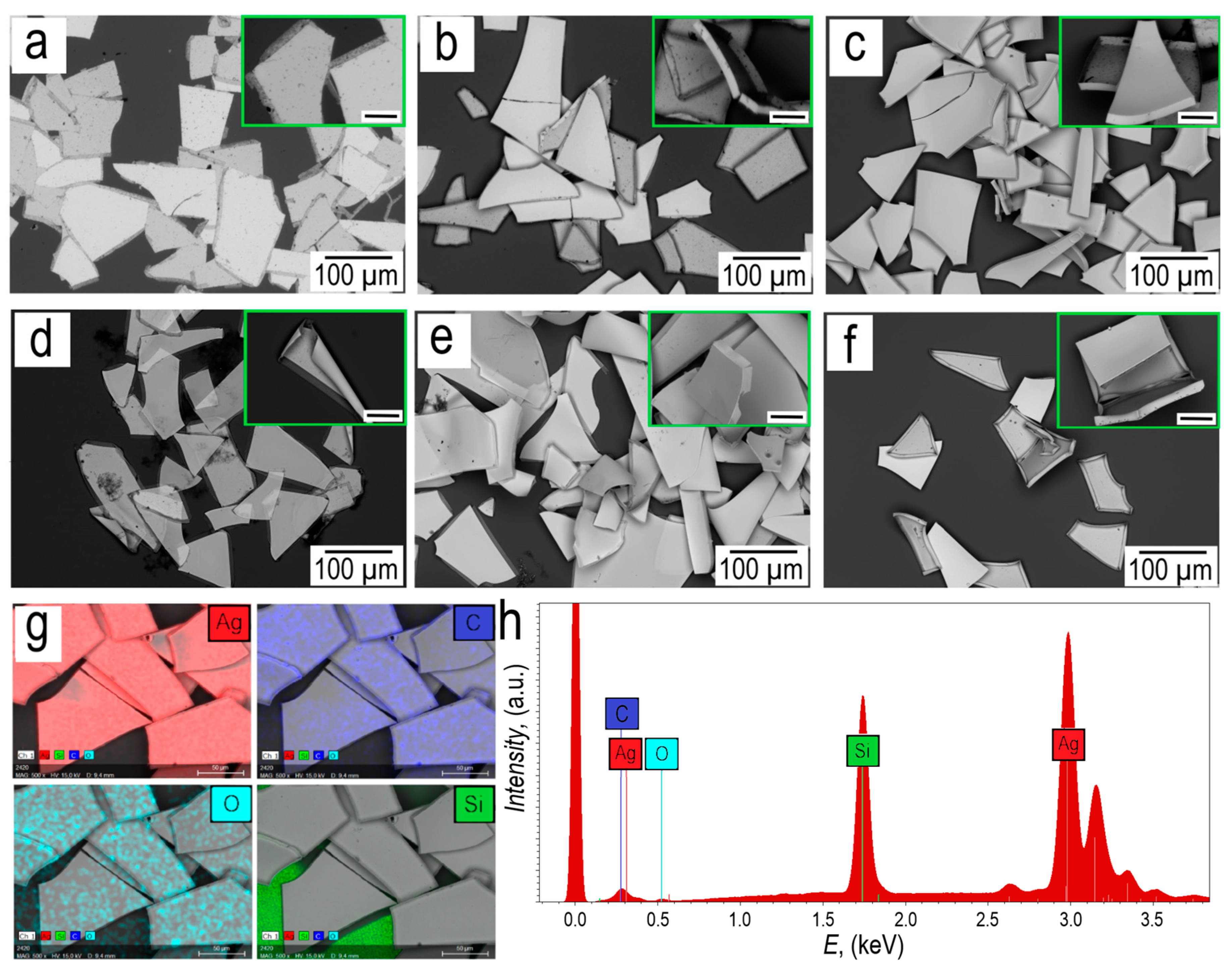
Figure 5 shows the
SEM image of silver micro caps of various thicknesses, which were obtained using magnetron and thermal deposition. The shape of single silver micro caps can be mathematically described by the Voronoi distribution [
64]
Based on the SEM images, it can be seen that the side faces of the silver micro caps for samples M-100 and T-100 can move freely. While side faces with a silver thickness of 300 nm and 600 nm, both in the case of thermal and magnetron deposition are rigid.
Elemental mapping is shown in
Figure 5h. Elemental analysis shows that, in addition to silver, silver micro caps contain traces of carbon and oxygen, which are most likely associated with underwashed egg white. The
EDX spectra in
Figure 5h show lines characteristic of Ag, namely the most intense peak with an energy of 2.983 keV corresponding to the
Lα1 series, peaks with energies of 3.150 keV and 3.347 keV belonging to the
Lβ1 and
Lβ2 series, respectively. A low-intensity peak with an energy of 3.520 keV corresponding to
Lγ1 is also observed. The peak with an energy of 0.277 keV corresponds to the
Kα1 series of carbon, and the peak with an energy of 0.525 keV corresponds to the
Kα1 series of oxygen. The low intensity of the carbon and oxygen peaks indicates a trace amount of residual egg white on the surface of the silver micro caps. A peak is also observed, which has an energy of 1.740 keV, this peak belongs to the
Kα1 series of the silicon substrate.
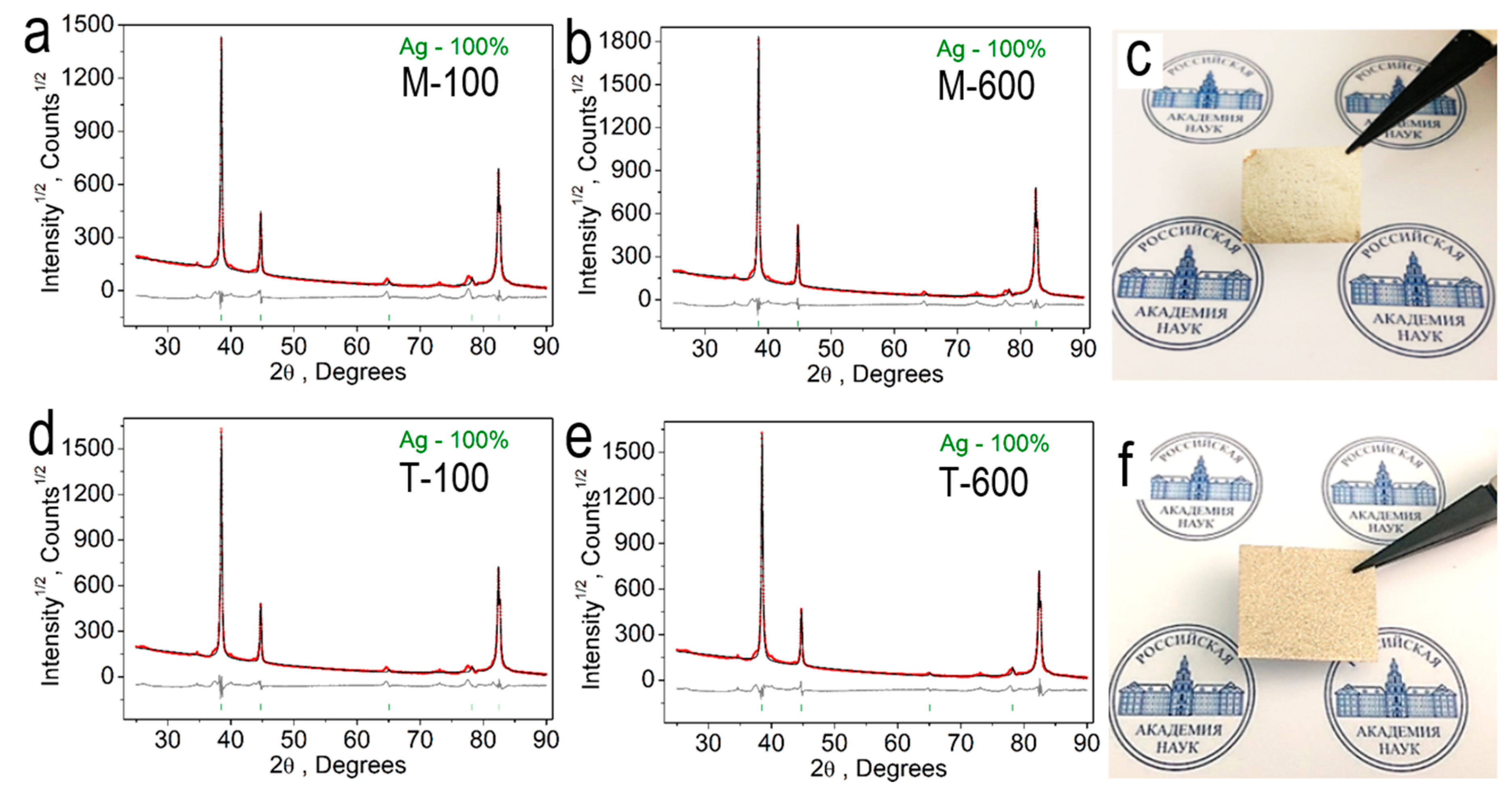
For further research, we formed films from silver micro caps by vacuum filtration. XRD patterns for silver micro caps films 100 nm and 600 nm thick are shown in
Figure 3d.
A complete analysis of the crystallographic parameters of all the described silver micro caps films is given in
Table 2. silver micro caps with a thickness of 100 and 600 nm, both obtained by both the magnetron and thermal methods, have a face-centered cubic crystal lattice, which belongs to the space group
Fm-3
m. The method of formation of silver microcaps does not affect their phase composition and structural composition.
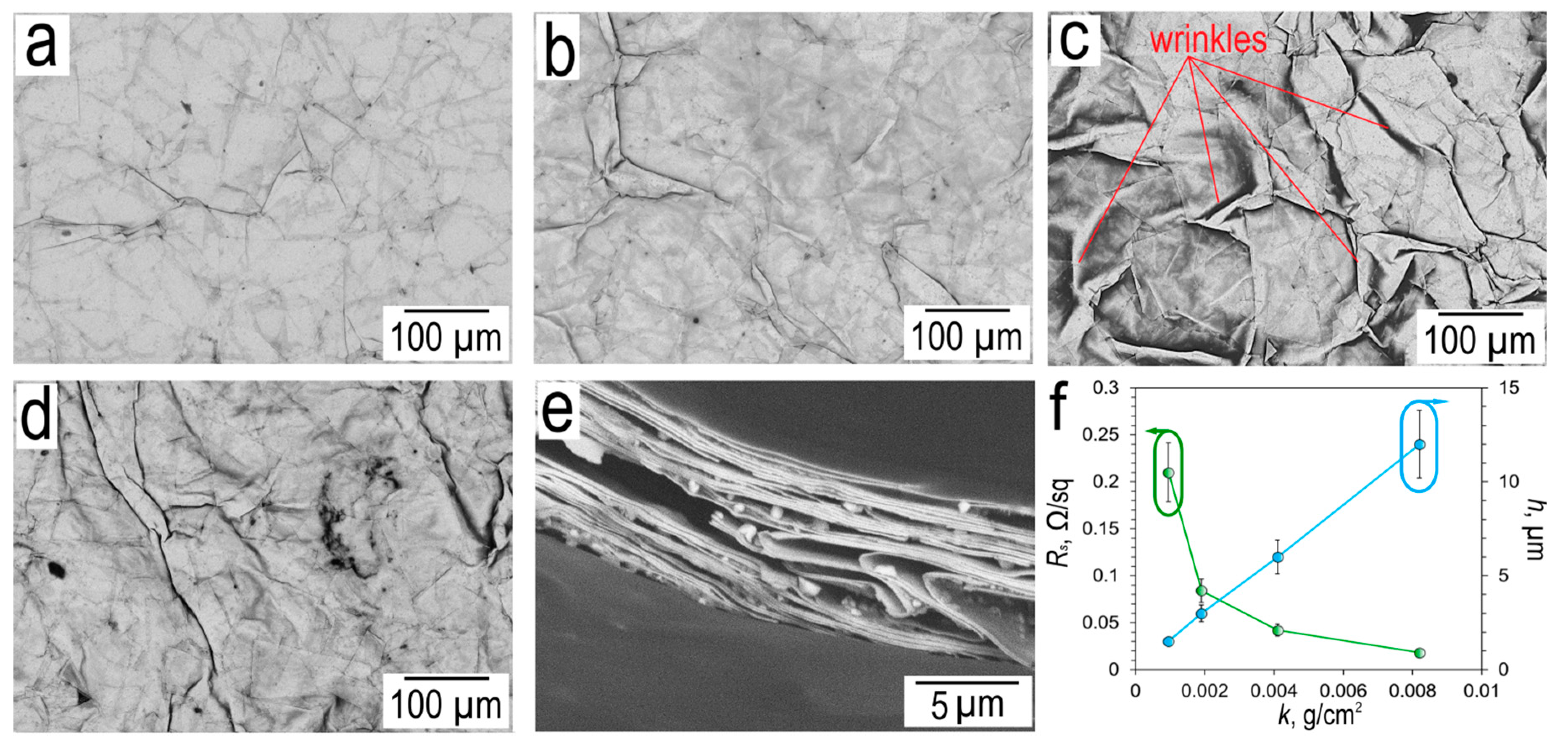
SEM images of the surface of silver micro caps films M-100 with different surface densities are shown in
Figure 7.
SEM images of silver micro caps films with different surface densities (
Figure 7a-d) show wrinkles that are typical for films of 2D materials such as rGO [
65], MXenes [
66]. The surface morphology of silver micro caps films is uniform and dense. The surface of the films is devoid of defects typical of such structures, which can include pores and holes. When analyzing the cross-section image of silver micro caps film M-100 with a surface density of ~4.1 mg/cm
2 (
Figure 7e), a layered structure can be observed, with air gaps between silver micro caps. This type of cross section is typical for metallic flakes films [
4].
On
Figure 7e shows thickness and sheet resistance versus surface density of silver micro caps M-100. Silver micro caps film with a surface density of 0.95 mg/cm
2 has a thickness of 1.5±0.3 µm, sheet resistance is 0.21±0.03 Ω/sq. The maximum surface density of the silver micro caps film obtained in this work is 8.2 mg/cm
2, its thickness is 12.2±2.4 µm at a sheet resistance of 0.018±0.003 Ω/sq. For electron transport in silver micro caps films, the key issue is the contact resistance between individual silver micro caps. In the case of silver micro caps with a perfectly clean surface, the contact between the two micro caps will be ohmic. The presence of adsorbed egg white molecules leads to the formation of a potential barrier. Iterative washing in DI water promotes the removal of a significant part of the adsorbed egg white, as evidenced by the low sheet resistance of silver micro caps films.
Under the conditions of roll2roll deposition, the proposed method makes it possible to obtain a significant amount of silver micro caps. Let’s evaluate the mass yield of silver micro caps, the mass of silver deposited on a flat substrate can be estimated by the formula m = ρSh, where S is the area that goes to micro caps, in the case of our cracked template, about 85% of the usable area goes to micro caps. Taking into account three thicknesses of sputtering and the fact that in one cycle a roll of 300 m long and 0.3 m wide can be sputtering (data based on our experience). The area of the roll described above is 90 m2, the area of the silver going to the micro caps is 76.5 m2. Thus, magnetron sputtering silver films with roll2roll process, we will obtain 76.5 g (M-100); 229.5 g (M-300); 459 g (M-600).
3.2.2. Separation of Silver Micro Caps into Silver Flakes and Ribbons and Their Morphological Features
The micro caps obtained by us are of interest in themselves as a new type of filler for electrically conductive composites, as well as for obtaining porous film structures (
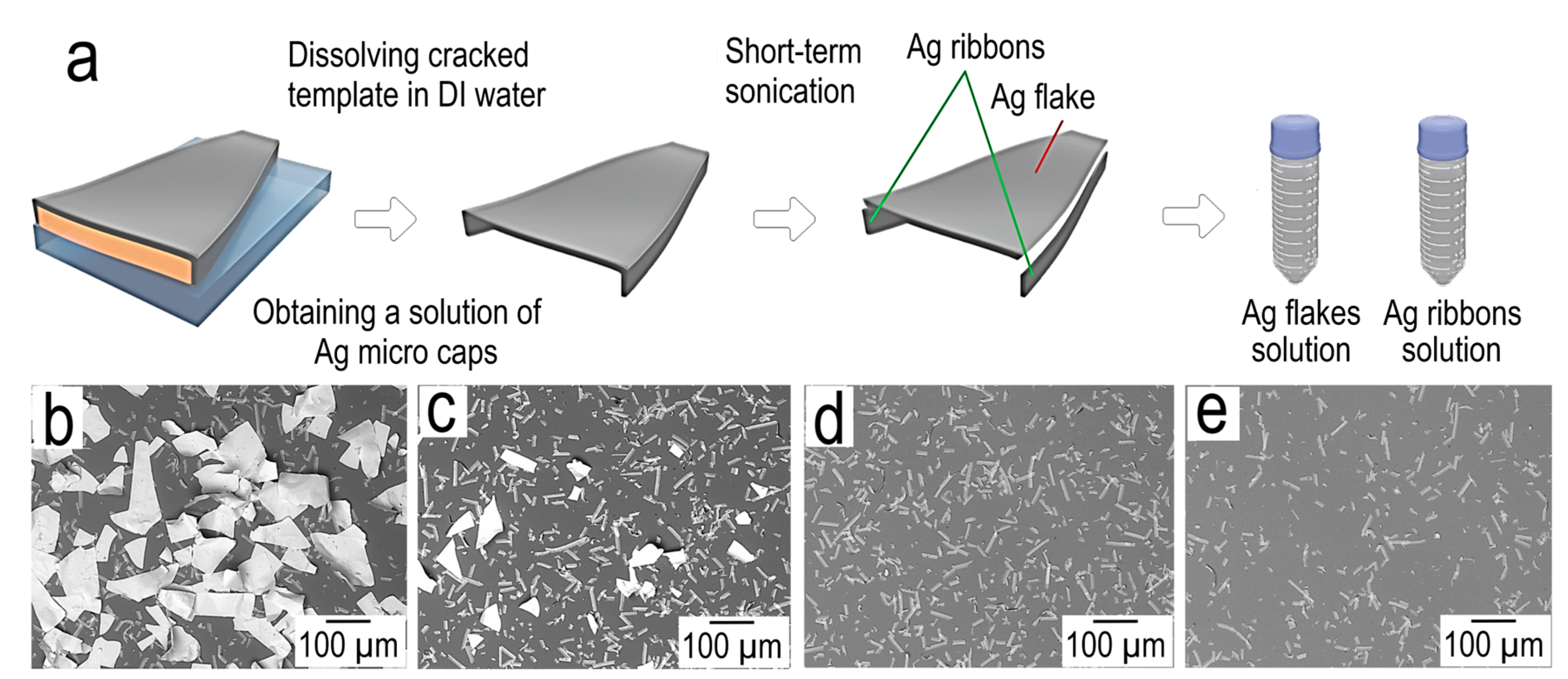
Figure 7). We found that short-term exposure to ultrasound on a solution of microcaps leads to their separation into flakes and ribbons.
Schematically, the process of separating micro caps into ribbons and flakes is shown in
Figure 8a
The
SEM image before the sedimentation fractionation operation (
Figure 8b) shows a clear separation of the micro caps material into ribbons and flakes. After 1 min of sediment separation (
Figure 8c), a significant reduction in flakes is observed. Small silver flakes are observed, as large silver flakes have a high sedimentation rate. After 5 min of sedimentation separation (
Figure 8d), silver flakes are absent in the deposit, only ribbons of various lengths are visible, which are significantly more resistant to sedimentation. A further increase in the sedimentation time to 15 min (
Figure 8e) demonstrates the presence of shorter ribbons than in
Figure 8d.
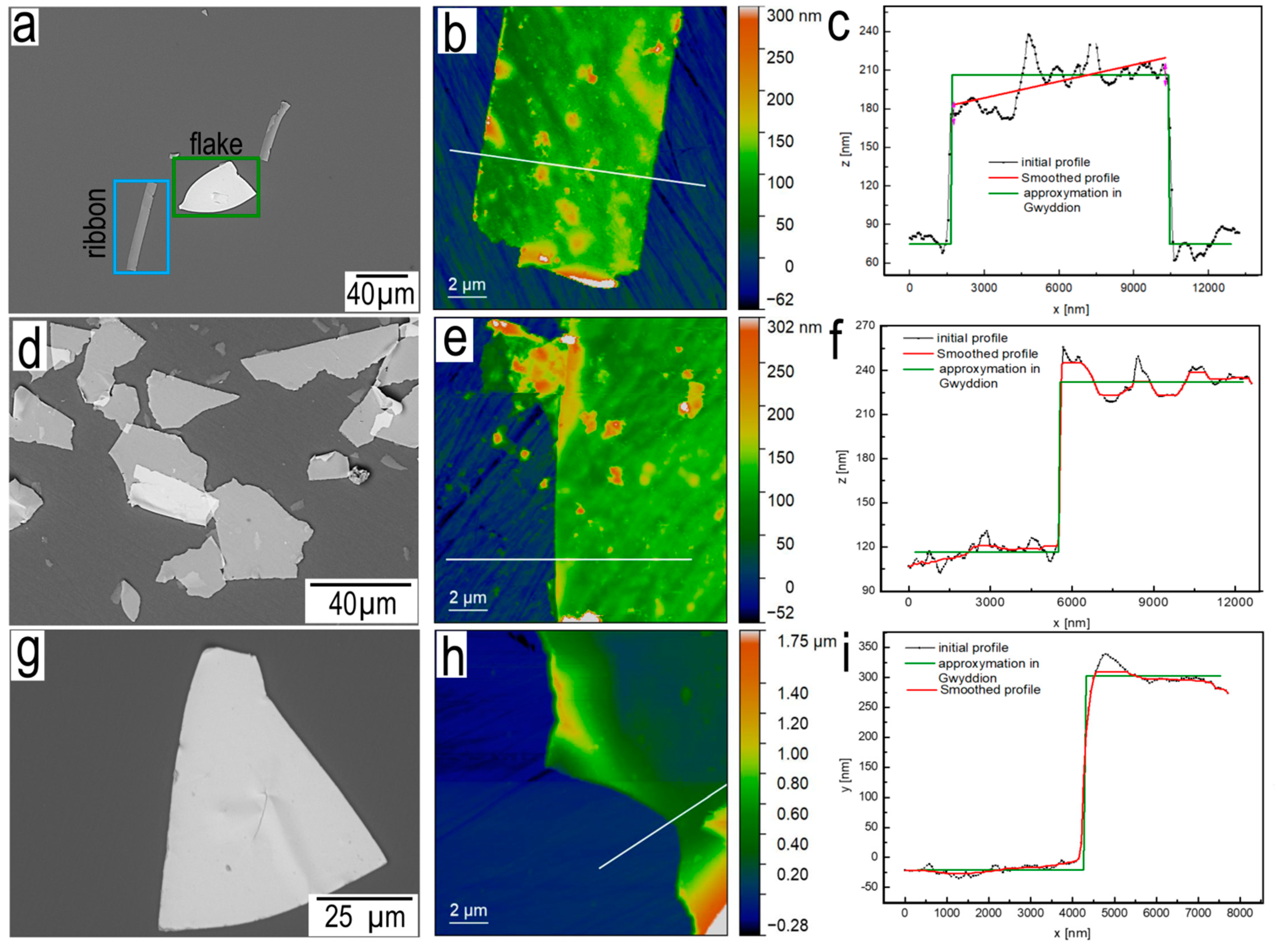
SEM and
AFM silver ribbons and silver flakes are shown in
Figure 9. Geometry of silver ribbons is characterized by the example of silver ribbons M-300, silver ribbons have a wedge geometry (
Figure 9b,c). At the junction of silver ribbon and silver flakes, the thickness of silver ribbons is ~135 nm, and its thickness uniformly decreases towards the bottom of the crack to ~105 nm.
Silver flakes T-100 (
Figure 9f) and T-300 (
Figure 9i) after approximation have a thickness of 100 nm and 300 nm, respectively. Thus, the thickness of flakes can be easily controlled, which is extremely difficult in the case of chemical synthesis of 2D materials. It is also worth noting the different resistance to ultrasound.
3.3. EMI Shielding Performance
The interaction of electromagnetic waves with matter occurs according to the following mechanism. The incident radiation is decomposed into three components: the reflected waves (
R), the absorbed waves (
A) and the transmitted waves (
T) (1), the sum of these three components is 1 (in (1) dimension of coefficients is [%]). Thus, the shielding of electromagnetic radiation is nothing more than the sum of losses for absorption (
A), reflection (
R) [
2]. Using the formalism of the scattering matrix and considering the waveguide-coaxial line as a two-terminal network, we can write the following formulas for the coefficients of reflection
R and transmission
T for material based on the coefficients of the scattering matrix for cell (2). The element of the scattering matrices
S11 correspond to the signal reflected from the sample, and the element
S21 correspond to the signal transmitted through the sample. These parameters are measured directly in the experiment, the dimension of these coefficients is [dB] (in (2) dimension of coefficients
T,
R is [dB]). According (2) coefficient of transmission
T is determined with
S21 of the cell with sample (
S21) and
S21 of empty cell (
S21norm), coefficient of reflection
R is determined with
S11 of the cell with sample (
S11) and
S11 of the cell with metallic sheet (
S11norm).
The value of the transmission coefficient
T may be transformed to the value of electromagnetic shielding efficiency (
SE) according to the formula (3).
3.3.1. Shielding and Reflecting Properties of Transparent Conductive Meshes Based on Cracked Template
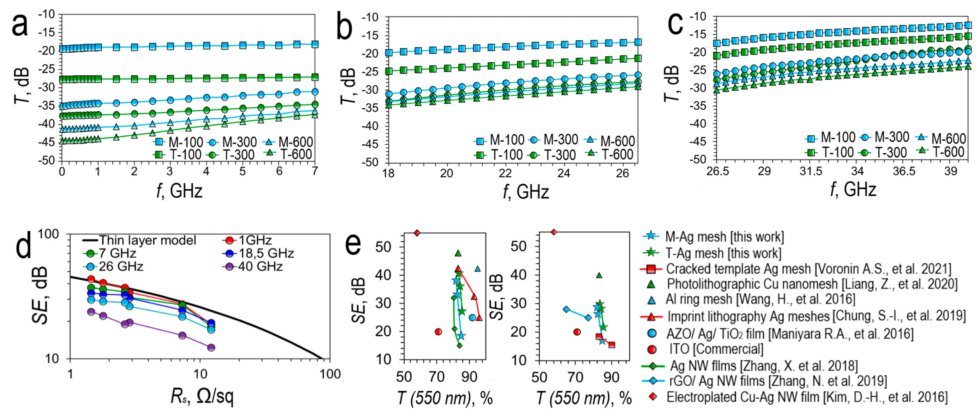
To determine the applicability of our transparent conductive meshes in 5G technologies as transparent shielding materials, transmission coefficients (
T) were measured in the following frequency bands
L (1-2 GHz),
S (2-4 GHz),
С (4-8 GHz) (
Figure 10a),
K (18-26.5 GHz) (
Figure 10b) and
Ka (26.5-40 GHz) (
Figure 10c).
For silver meshes based on magnetron sputtering and based on thermal sputtering, similar
T dependences are observed, taking into account that the shielding effect is higher for silver meshes obtained using thermal sputtering due to lower sheet resistance. The minimum transmission is observed at a frequency of 10 MHz, it is -41.25 dB (M-600) and -44.43 dB (T-600), then the transmission increases uniformly with increasing frequency of the incident wave. This behavior is typical for meshes [
36,
37,
38]. For silver meshes with a sheet resistance greater than 5 Ω/sq (silver meshes M-100 and T-100), the frequency dependence of the transmittance is weaker in the low-frequency region than for lower sheet resistance silver meshes (
Figure 10a). In the high-frequency region, the slope of the transmission curves is approximately the same for all types of silver meshes (
Figure 10b,c).
Figure 10d compares our silver meshes with the thin layer model at 1 GHz, 7 GHz, 18 GHz, 26 GHz, and 40 GHz. At a frequency of 1 GHz, the entire sample of silver meshes is in good agreement with the continuous layer model, which indicates that at these frequencies the aperture effects are negligible. A gradual increase in frequency leads to an increase in the discrepancy with the continuous layer model.
As was shown in [
37], at frequencies above 8 GHz Cu-Ag meshes are weakly agreement with the continuous layer model, our silver meshes are also agreement with the continuous layer model only at frequencies up to 1 GHz, this trend was also observed in [
38].
On
Figure 10e shows a comparative graph of
SE versus transparency for the most promising coatings in the literature at frequencies of 3.5 GHz and 26 GHz, these frequencies are allocated for 5G communication. At a frequency of 3.5 GHz, our silver meshes show a high
SE value, silver mesh T-600 has a
SE of 41.56 dB, which is comparable to nanomeshes obtained by photolithography [
32] and imprint lithography [
36]. At a frequency of 26 GHz, our silver mesh T-600 has a
SE of 29.38 dB, yielding in efficiency only to the photolithographic Cu nanomesh [
32] due to the fact that our silver meshes have a much larger average cell size.
As a rule, two types of transparent shielding materials are currently used in practice. Firstly, these are metal meshes with a period of 500–1000 µm and a track width of 25–50 µm. Such coatings have a high shielding ability at frequencies below 1 GHz (>50 dB), which quickly decreases at frequencies above 1 GHz and, as a rule, does not exceed 30 dB at 10 GHz. A further increase in the frequency of the incident radiation leads to a strong drop in the screening capacity, so, according to [
32], at a frequency of 26 GHz, a grid with a cell of 1.2 mm will have a screening capacity of no more than 10 dB. Secondly, these are TCO films, for example, ITO is most often used, which has a weak frequency dependence, and is characterized by a shielding efficiency of ~20 dB in the 1-40 GHz range.
In addition to shielding, a high reflection coefficient from the coating is important in 5G communication in order to maintain an acceptable signal level by reflecting from wall surfaces, billboards, etc. [
42].
Figure 11 shows the spectral dependences of the reflection coefficient in the ranges
L (1-2 GHz) and
S (2-4 GHz) and
C (4-8 GHz) (
Figure 11a),
K (18.5-26.5 GHz) (
Figure 11b) and
Ka (26.5-40 GHz) (
Figure 11c).
Increasing the thickness of the sputtered metal increases the reflection coefficient for silver meshes both in the case of magnetron and thermal deposition. Magnetron sputtered silver meshes have reflectance values at 3.5 GHz of -1.06 dB (78.3%) (M-100), -0.174 dB (96.1%) (M-300) and -0.11 dB (97.5%) (M-600) respectively. At 26 GHz, the reflectance is -1.27 dB (74.6%), -0.34 dB (92.5%); -0.17dB (96.2%). For thermal sputtering silver meshes, the reflection coefficient at 3.5 GHz is -0.42 dB (90.8%) (T-100), -0.152 dB (96.6%) (T-300), -0.067dB (98.5%) (T -600). At 26 GHz, the reflectance is -0.67 dB (85.7%), -0.29 dB (93.5%), -0.14dB (96.8%). According to the measurement results, silver meshes with a thickness of 300 and 600 nm at frequencies of 3.5 GHz and 26 GHz have a reflection coefficient of more than 92%, both in the case of magnetron and thermal deposition. As with shielding, silver meshes obtained by thermal sputtering show the best reflectance coefficient due to the lower sheet resistance.
3.3.2. Silver Micro Caps Films
As shown above (
Figure 7), silver micro caps films based, M-100 have a low sheet resistance comparable to the literature results [
4]. This fact makes silver micro caps films interesting objects for study in order to obtain shielding materials operating in a wide frequency range, including 5 G. To confirm the above assumptions, we study the spectral characteristics of silver micro caps films M-100 in a wide frequency range.
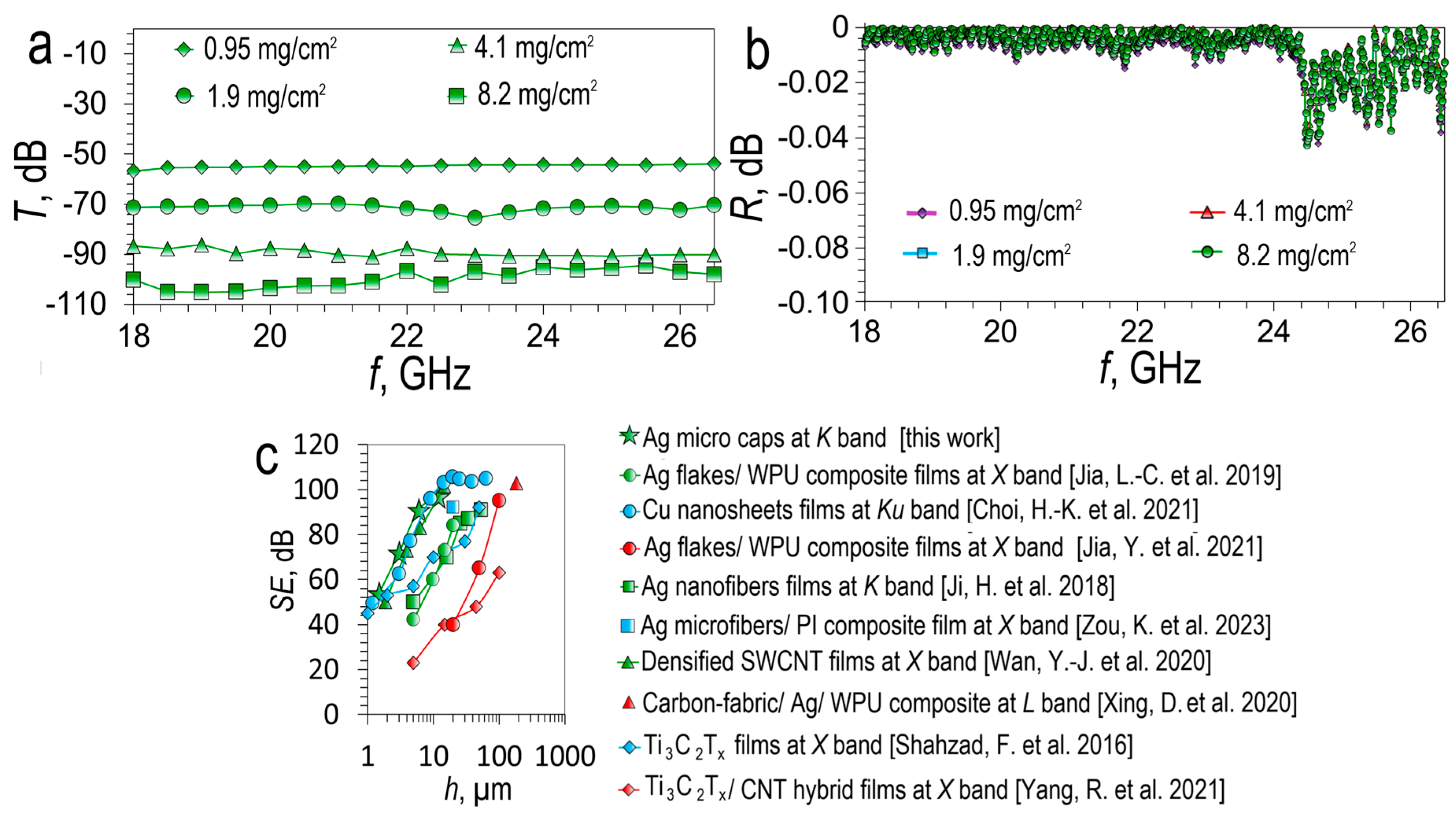
Figure 12 shows the spectral dependences of the transmittance (
T) (
Figure 12a) and reflectance (
R) (
Figure 12b) for silver micro caps films M-100 of various surface density in the
K range (18-26.5 GHz) (
Figure 12b)
A successive increase in the silver micro caps film thickness from 1.5±0.3 to 12±2.4 µm promotes an increase in
SE from ~54.13 dB to ~97.06 dB. In the entire considered frequency range, the transmission is uniform, in contrast to silver meshes. The main shielding mechanism is reflection (
Figure 12b) according to the graph, all micro caps films have a reflectance greater than 99%. Based on the comparison plot (
Figure 12), it can be seen that our silver micro caps films in
SE(h) coordinates correlate with the most promising results from the literature, such as Cu nanosheets porous films [
4] and densified SWCNT films [
77]. The main reason for such a high SE value is the low sheet resistance, which is significantly lower than for MXenes, SWCNT films, and polymer composites with various types of fillers.
As a summary, we can conclude that silver micro caps are highly promising for the formation of film structures, bulk polymer composites, and composite coatings with a high shielding factor.
4. Conclusion
In this work, we presented the concept of an environmentally friendly, waste-free, cost-effective technology for the production of materials for 5 G communication. It is shown that each of the two types of obtained materials demonstrates high shielding efficiency at the main frequencies corresponding to 5G communication. The first material is a transparent conductive silver mesh, which has a shielding efficiency at 3.5 GHz is 41.56 dB (T-600), at 26 GHz it is 29.38 dB (T-600). Silver mesh transparent conductor based on cracked template, can be used as passive 5G signal reflectors, in order to compensate for signal loss when interacting with urban objects, it is shown that the silver mesh T-600 sample has a reflectance of 98.5% at a frequency of 3.5 GHz and 96.6% at a frequency of 26 GHz.
The second type of material obtained in this work is a thin film of Ag micro caps. Such a film has an SE value of 90.1 dB at a thickness of 6.2±1.2 µm.
Author Contributions
Conceptualization: A.S.V., Y.V.F., F.S.I., S.V.K.; experiment and data analysis: A.S.V., Y.V.F., M.O.M., P.A.M., D.S.R., G.Y.Y., D.V.K., A.V.L., K.A.S., M.S.M.; synthesis: A.S.V., I.A.T., S.V.N., N.A.Z. and D.D.B.; writing–original draft preparation: A.S.V., M.O.M. and I.A.D.; writing–review and editing: A.S.V., M.O.M., D.S.R. and M.M.S.; project administration: S.V.K. and P.A.M. All authors have read and agreed to the published version of the manuscript.
Funding
This research work was supported by the Ministry of Science and Higher Education of the Russian Federation within the framework of state tasks FWES-2021-0026 and No. FSFN-2022-0007.
Institutional Review Board Statement
Not applicable.
Informed Consent Statement
Not applicable.
Data Availability Statement
Not applicable.
Acknowledgments
The development of processes for the synthesis of a cracked template, the preparation and purification of silver micro caps, study electrical and shielding properties of silver micro caps films was supported financially within the state assignment FWES-2021-0026 of Federal Research Center Krasnoyarsk Science Center of the Siberian Branch of the Russian Academy of Sciences. The development of the processes of the formation of silver mesh transparent conductor and the study of the structural, optical, electrical and shielding properties of the samples were carried out with the financial support of the Ministry of Science and Higher Education of the Russian Federation within the framework of state assignment No. FSFN-2022-0007. The physicochemical analysis of materials was carried out on equipment from the Krasnoyarsk Regional Center of Research Equipment of Federal Research Center «Krasnoyarsk Science Center SB RAS».
References
- Tong, C. (2022). EMI Shielding Materials and Absorbers for 5G Communications. In: Advanced Materials and Components for 5G and Beyond. Springer Series in Materials Science, vol 327. Springer, Cham. [CrossRef]
- Geetha, S.; Satheesh Kumar, K.K.; Rao, Chepuri, R.K.; Vijayan, M.; Trivedi, D.C. EMI Shielding: Methods and Materials—A Review. Journal of Applied Polymer Sci. 2009, 112, 2073–2086. [CrossRef]
- Wanasinghe, D.; Aslani, F. A review on recent advancement of electromagnetic interference shielding novel metallic materials and processes. Composites Part B: Engineering 2019, 176, 107207. [Google Scholar] [CrossRef]
- Choi, H.K.; Lee, A.; Park, M.; Lee, D.S.; Bae, S.; Lee, S.-K.; Lee, S.H.; Lee, T.; Kim, T.-W. Hierarchical Porous Film with Layer-by-Layer Assembly of 2D Copper Nanosheets for Ultimate Electromagnetic Interference Shielding. ACS Nano 2021, 15, 829–839. [Google Scholar] [CrossRef] [PubMed]
- Sahoo, R.; Sundara, R.; Venkatachalam, S. Silver Nanowires Coated Nitrocellulose Paper for High-Efficiency Electromagnetic Interference Shielding. ACS Omega 2022, 7, 41426–41436. [Google Scholar] [CrossRef] [PubMed]
- Kumar, R.; Sahoo, S.; Joanni, E.; Singh, R.K.; Tan, W.K.; Kar, K.K.; Matsuda, A. Recent progress on carbon-based composite materials for microwave electromagnetic interference shielding. Carbon 2021, 177, 304–331. [Google Scholar] [CrossRef]
- Yang, Y.; Gupta, M.C.; Dudley, K.L.; Lawrence, R.W. Novel Carbon Nanotube−Polystyrene Foam Composites for Electromagnetic Interference Shielding. Nano Lett. 2005, 5, 2131–2134. [Google Scholar] [CrossRef]
- Wan, Y.-J.; Zhu, P.-L.; Yu, S.-H.; Sun, R.; Wong, C.-P.; Liao, W.-H. Graphene paper for exceptional EMI shielding performance using large-sized graphene oxide sheets and doping strategy. Carbon 2017, 122, 74–81. [Google Scholar] [CrossRef]
- Munalli, D.; Dimitrakis, G.; Chronopoulos, D.; Greedy, S.A. Long Electromagnetic shielding effectiveness of carbon fibre reinforced composites. Composites Part B: Engineering 2019, 173, 106906. [Google Scholar] [CrossRef]
- Zhou, E.; Xi, J.; Guo, Y.; Liu, Y.; Xu, Z.; Peng, L.; Gao, W.; Ying, J.; Chen, Z.; Gao, C. Synergistic effect of graphene and carbon nanotube for high-performance electromagnetic interference shielding films. Carbon 2018, 133, 316–322. [Google Scholar] [CrossRef]
- Shahzad, F.; Alhabeb, M.; Hatter, C.B.; Anasori, B.; Hong, S.M.; Koo, C.M.; Gogotsi, Y. Electromagnetic interference shielding with 2D transition metal carbides (MXenes). Science 2016, 353, 1137–1140. [Google Scholar] [CrossRef]
- Iqbal, A.; Sambyal, P.C.; Koo, M. 2D MXenes for Electromagnetic Shielding: A Review. Adv. Funct. Mater. 2020, 30, 2000883. [Google Scholar] [CrossRef]
- Han, M.; Shuck, C.E.; Rakhmanov, R.; Parchment, D.; Anasori, B.; Koo, C.M.; Friedman, G.; Gogotsi, Y. Beyond Ti3C2Tx: MXenes for Electromagnetic Interference Shielding. ACS Nano 2020, 14, 5008–5016. [Google Scholar] [CrossRef] [PubMed]
- Li, Z.; Wang, Z.; Lu, W.; Hou, B. Theoretical Study of Electromagnetic Interference Shielding of 2D MXenes Films. Metals 2018, 8, 652. [Google Scholar] [CrossRef]
- Shukla,V. Review of electromagnetic interference shielding materials fabricated by iron ingredients. Nanoscale Adv. 2019, 1, 1640–1671. [Google Scholar] [CrossRef]
- Dong, J.; Ullal, R.; Han, J.; Wei, S.; Ouyang, X.; Donga, Gao, J.W. Partially crystallized TiO2 for microwave absorption. J. Mater. Chem. A 2015, 3, 5285–5288. [CrossRef]
- Maruthi, N.; Faisal, M.; Raghavendra, N. Conducting polymer based composites as efficient EMI shielding materials: A comprehensive review and future prospects. Synthetic Metals. 2021, 272, 116664. [Google Scholar] [CrossRef]
- Yun, T.; Kim, H.; Iqbal, A.; Cho, Y.S.; Lee, G.S.; Kim, M.-K.; Kim, S.J.; Kim, D.; Gogotsi, Y.; Kim, S.O.; Koo, C.M. Electromagnetic Shielding of Monolayer MXene Assemblies. Adv. Mater. 2020, 32, 1906769. [Google Scholar] [CrossRef]
- Wei, Z.; Huagang, X.; Shaokai, W.; Min, L.; Yizhuo, G. Electromagnetic characteristics of carbon nanotube film materials. Chinese Journal of Aeronautics. 2015, 28, 1245–1254. [Google Scholar] [CrossRef]
- Liang, C.; Gu, Z.; Zhang, Y.; Ma, Z.; Qiu, H.; Gu, J. Structural Design Strategies of Polymer Matrix Composites for Electromagnetic Interference Shielding: A Review. Nano-Micro Lett. 2021, 13, 181. [Google Scholar] [CrossRef]
- Wang, H.; Zheng, K.; Zhang, X.; Wang, Y.; Xiao, C.; Chen, L.; Tian, X. Hollow microsphere-infused porous poly(vinylidene fluoride)/multiwall carbon nanotube composites with excellent electromagnetic shielding and low thermal transport. J Mater Sci 2018, 53, 6042–6052. [Google Scholar] [CrossRef]
- Wanasinghe, D.; Aslani, F.; Ma, G.; Habibi, D. Review of Polymer Composites with Diverse Nanofillers for Electromagnetic Interference Shielding. Nanomaterials 2020, 10, 541. [Google Scholar] [CrossRef] [PubMed]
- Ha, J.-H.; Hong, S.-K.; Ryu, J.-K.; Bae, J.; Park, S.-H. Development of Multi-Functional Graphene Polymer Composites Having Electromagnetic Interference Shielding and De-Icing Properties. Polymers 2019, 11, 2101. [Google Scholar] [CrossRef] [PubMed]
- Ahmad, A.F.; Ab Aziz, S.; Abbas, Z.; Obaiys, S.J.; Khamis, A.M.; Hussain, I.R.; Zaid, M.H.M. Preparation of a Chemically Reduced Graphene Oxide Reinforced Epoxy Resin Polymer as a Composite for Electromagnetic Interference Shielding and Microwave-Absorbing Applications. Polymers 2018, 10, 1180. [Google Scholar] [CrossRef]
- Wang, Y.-Y.; Zhang, F.; Li, N.; Shi, J.-F.; Jia, L.-C.; Yan, D.-X.; Li, Z.-M. Carbon-based aerogels and foams for electromagnetic interference shielding: A review. Carbon 2023, 205, 10–26. [Google Scholar] [CrossRef]
- Zeng, Z.; Wu, T.; Han, D.; Ren, Q.; Siqueira, G.; Nyström, G. Ultralight, Flexible, and Biomimetic Nanocellulose/Silver Nanowire Aerogels for Electromagnetic Interference Shielding. ACS Nano 2020, 14, 2927–2938. [Google Scholar] [CrossRef] [PubMed]
- Du,Y.; Xu, J.; Fang, J.; Zhang, Y.; Liu, X.; Zuo, P.; Zhuang, Q. Ultralight, highly compressible, thermally stable MXene/aramid nanofiber anisotropic aerogels for electromagnetic interference shielding. J. Mater. Chem. A 2022, 10, 6690–6700. [CrossRef]
- Blachowicz, T.; Wójcik, D.; Surma, M.; Magnuski, M.; Ehrmann, G.; Ehrmann, A. Textile Fabrics as Electromagnetic Shielding Materials—A Review of Preparation and Performance. Fibers 2023, 11, 29. [Google Scholar] [CrossRef]
- Yao, B.; Xu, X.; Li, H.; Han, Z.; Hao, J.; Yang, G.; Xie, Z.; Chen, Y.; Liu, W.; Wang, Q.; Wang, H. Soft liquid-metal/elastomer foam with compression-adjustable thermal conductivity and electromagnetic interference shielding. Chemical Engineering Journal 2021, 410, 128288. [Google Scholar] [CrossRef]
- Luo, H.; Chen, F.; Wang, X.; Dai, W.; Xiong, Y.; Yang, J.; Gong, R. A novel two-layer honeycomb sandwich structure absorber with high-performance microwave absorption. Composites Part A: Applied Science and Manufacturing 2019, 119, 1–7. [Google Scholar] [CrossRef]
- Li, Q.; Bi, S.; Wang, X.; Song, J. Development and current situation of flexible and transparent EM shielding materials. J Mater Sc. Mater Electron 2021, 32, 25603–25630. [Google Scholar] [CrossRef]
- Liang, Z.; Zhao, Z.; Pu, M.; Luo, J.; Xie, X.; Wang, Y.; Guo, Y.; Ma, X.; Luo, X. Metallic nanomesh for high-performance transparent electromagnetic shielding. Opt. Mater. Express 2020, 10, 796. [Google Scholar] [CrossRef]
- Liang, Y.; Huang, X.; Wen, K.; Wu, Z.; Yao, L.; Pan, J.; Liu, W.; Liu, P. Metal Mesh-Based Infrared Transparent EMI Shielding Window with Balanced Shielding Properties over a Wide Frequency Spectrum. Appl. Sci. 2023, 13, 4846. [Google Scholar] [CrossRef]
- Osipkov, A.; Makeev, M.; Konopleva, E.; Kudrina, N.; Gorobinskiy, L.; Mikhalev, P.; Ryzhenko, D.; Yurkov, G. Optically Transparent and Highly Conductive Electrodes for Acousto-Optical Devices. Materials 2021, 14, 7178. [Google Scholar] [CrossRef] [PubMed]
- Chung, S.-I.; Kim, P.K.; Ha, T.-G.; Han, J.T. High-performance flexible transparent nanomesh electrodes. Nanotechnology, 2019, 30, 125301. [Google Scholar] [CrossRef]
- Han, Y.; Lin, J.; Liu, Y.; Fu, H.; Ma, Y.; Jin, P.; Tan, J. Crackle template based metallic mesh with highly homogeneous light transmission for high-performance transparent EMI shielding. Sci. Rep. 2016, 6, 25601. [Google Scholar] [CrossRef]
- Voronin, A.S.; Fadeev, Y.V.; Govorun, I.V.; Podshivalov, I.V.; Simunin, M.M.; Tambasov, I.A.; Karpova, D.V.; Smolyarova, T.E.; Lukyanenko, A.V.; Karacharov, A.A.; et al. Cu–Ag and Ni–Ag meshes based on cracked template as efficient transparent electromagnetic shielding coating with excellent mechanical performance. J. Mater. Sci. 2021, 56, 14741–14762. [Google Scholar] [CrossRef]
- Voronin, A.S.; Fadeev, Y.V.; Makeev, M.O.; Mikhalev, P.A.; Osipkov, A.S.; Provatorov, A.S.; Ryzhenko, D.S.; Yurkov, G.Y.; Simunin, M.M.; Karpova, D.V.; Lukyanenko, A.V.; Kokh, D.; Bainov, D.D.; Tambasov, I.A.; Nedelin, S.V.; Zolotovsky, N.A.; Khartov, S.V. Low Cost Embedded Copper Mesh Based on Cracked Template for Highly Durability Transparent EMI Shielding Films. Materials 2022, 15, 1449. [Google Scholar] [CrossRef]
- Hu, M.; Gao, J.; Dong, Y.; Li, K.; Shan, G.; Yang, S.; Li, R.K.-Y. Flexible Transparent PES/Silver Nanowires/PET Sandwich-Structured Film for High-Efficiency Electromagnetic Interference Shielding. Langmuir 2012, 28, 7101–7106. [Google Scholar] [CrossRef]
- Zhu, X.; Guo, A.; Yan, Z.; Qin, F.; Xu, J.; Ji, Y.; Kan, C. PET/Ag NW/PMMA transparent electromagnetic interference shielding films with high stability and flexibility. Nanoscale 2021, 13, 8067. [Google Scholar] [CrossRef]
- Khawaja, W.A.G.; Ozdemir, O.; Erden, F.; Guvenc, I.; Ezuma, M.; Kakishima, Y. Effect of Passive Reflectors for Enhancing Coverage of 28 GHz mmWave Systems in an Outdoor Setting. Proc. 2019 IEEE Radio and Wireless Symposium (RWS), January 2019. [CrossRef]
- Khawaja, W.; Ozdemir, O.; Yapici, Y.; Erden, F.; Ezuma, M.; Guvenc, I. Coverage Enhancement for NLOS mmWave Links Using Passive Reflectors. IEEE Open Journal of the Communications Society, 2020, 1, 263–281. [Google Scholar] [CrossRef]
- Anjinappa, C.K.; Ganesh, A.P.; Ozdemir, O.; Ridenour, K.; Khawaja, W.; Guvenc, ˙I.; Nomoto, H.; Ide, Y. Indoor Propagation Measurements with Transparent Reflectors at 28/39/120/144 GHz. Proc. 2022 IEEE International Conference on Communications Workshops (ICC Workshops), May 2022. [CrossRef]
- Voronin, A.S.; Fadeev, Y.V.; Ivanchenko, F.S.; Dobrosmyslov, S.S.; Makeev, M.O.; Mikhalev, P.A.; Osipkov, A.S.; Damaratsky, I.A.; Ryzhenko, D.S.; Yurkov, G.Y.; Simunin, M.M.; Volochaev, M.N.; Tambasov, I.A.; Nedelin, S.V.; Zolotovsky, N.A.; Bainov, D.D.; Khartov, S.V. Original concept of cracked template with controlled peeling of the cells perimeter for high performance transparent EMI shielding films. Surf. and Interfaces 2023, 38, 102793. [Google Scholar] [CrossRef]
- Voronin, A.S.; Simunin, M.M.; Fadeev, Y.V.; Ivanchenko, F.S.; Karpova, D.V.; Tambasov, I.A.; Khartov, S.V. Technological Basis of the Formation of Micromesh Transparent Electrodes by Means of a Self-Organized Template and the Study of Their Properties. Tech. Phys. Lett. 2019, 45, 366–369. [Google Scholar] [CrossRef]
- Voronin, A.S.; Fadeev, Y.V.; Dobrosmyslov, S.S.; Simunin, M.M.; Khartov, S.V. Random Ag mesh transparent heater obtained with a cracked template technique. J. Phys.: Conf. Ser. 2020, 1679, 042087. [Google Scholar] [CrossRef]
- Kiruthika, S.; Rao, K.D.M.; Kumar, A.; Gupta, R.; Kulkarni, G.U. Metal wire network based transparent conducting electrodes fabricated using interconnected crackled layer as template. Mater Res Express 2014, 1, 026301. [Google Scholar] [CrossRef]
- Kiruthika, S.; Gupta, R.; Rao, K.D.M.; Chakraborty, S.; Padmavathy, N.; Kulkarni, G.U. Large area solution processed transparent conducting electrode based on highly interconnected Cu wire network. J Mater Chem C 2014, 2, 2089–2094. [Google Scholar] [CrossRef]
- Han, Y.; Liu, Y.X.; Han, L.; Lin, J.; Jin, P. High-performance hierarchical graphene/metal-mesh film for optically transparent electromagnetic interference shielding. Carbon 2017, 115, 34–42. [Google Scholar] [CrossRef]
- Kim, Y.-g.; Tak, Y.J.; Park, S.P.; Kim, H.J.; Kim, H.J. Structural Engineering of Metal-Mesh Structure Applicable for Transparent Electrodes Fabricated by Self-Formable Cracked Template. Nanomaterials 2017, 7, 214. [Google Scholar] [CrossRef]
- Lee, H.B.; Jin, W.-Y.; Ovhal, M.M.; Kumar, N.; Kang, J.-W. Flexible transparent conducting electrodes based on metal meshes for organic optoelectronic device applications: a review. J Mater Chem C 2019, 7, 1087–1110. [Google Scholar] [CrossRef]
- Jung, J.; Lee, H.; Ha, I.; Cho, H.; Kim, K.K.; Kwon, J.; Won, P.; Hong, S.; Ko, S.H. Highly Stretchable and Transparent Electromagnetic Interference Shielding Film Based on Silver Nanowire Percolation Network for Wearable Electronics Applications. ACS Appl. Mater. Interfaces 2017, 9, 44609–44616. [Google Scholar] [CrossRef]
- Wu, H.; Kong, D.; Ruan, Z.; Hsu, P.-C.; Wang, S.; Yu, Z.; Carney, T.J.; Hu, L.; Fan, S.; Cui, Y. A transparent electrode based on a metal nanotrough network. Nature Nanotech 2013, 8, 421–425. [Google Scholar] [CrossRef]
- Deng, B.; Hsu, P.-C.; Chen, G.; Chandrashekar, B.N.; Liao, L.; Ayitimuda, Z.; Wu, J.; Guo, Y.; Lin, L.; Zhou, Y.; Aisijiang, M.; Xie, Q.; Cui, Y.; Liu, Z.; Peng, H. Roll-to-Roll Encapsulation of Metal Nanowires between Graphene and Plastic Substrate for High-Performance Flexible Transparent Electrodes. Nano Lett. 2015, 15, 4206–4213. [Google Scholar] [CrossRef] [PubMed]
- Jang, J.; Hyun, B.G.; Ji, S.; Cho, E.; An, B.W.; Cheong, W.H.; Park, J.-U. Rapid production of large-area, transparent and stretchable electrodes using metal nanofibers as wirelessly operated wearable heaters. NPG Asia Mater. 2017, 9, e432. [Google Scholar] [CrossRef]
- Kim, H.-J.; Kim, Y.; Jeong, J.-H.; Choi, J.-H.; Lee, J.; Choi, D.-G. A cupronickel-based micromesh film for use as a high-performance and low-voltage transparent heater. J. Mater. Chem. A 2015, 3, 16621–16626. [Google Scholar] [CrossRef]
- Bae, S.; Kim, H.; Lee, Y.; Xu, X.F.; Park, J.S.; Zheng, Y.; Balakrishnan, J.; Lei, T.; Kim, H.R.; Song, Y.I.; Kim, Y.J.; Kim, K.S.; Ozyilmaz, B.; Ahn, J.H.; Hong, B.H.; Iijima, S. Roll-to-roll production of 30-inch graphene films for transparent electrodes. Nat Nanotechnol. 2010, 5, 574–578. [Google Scholar] [CrossRef] [PubMed]
- Tian, Y.; Guo, N.; Wang, W.-Y.; Geng, W.; Jing, L.-C.; Wang, T.; Yuan, X.-T.; Zhu, Z.; Ma, Y.; Geng, H.-Z. Bilayer and three dimensional conductive network composed by SnCl2 reduced rGO with CNTs and GO applied in transparent conductive films. Sci Rep, 2021, 11, 9891. [Google Scholar] [CrossRef] [PubMed]
- Wang, H.; Yang, W.; Liab, K.; Li, G. The hydrothermal synthesis of ultra-high aspect ratio Ag nanoflakes and their performance as conductive fillers in heaters and pastes. RSC Adv. 2018, 8, 8937. [Google Scholar] [CrossRef]
- Rosen, Y.; Marrach, R.; Gutkin, V.; Magdassi, S. Thin Copper Flakes for Conductive Inks Prepared by Decomposition of Copper Formate and Ultrafine Wet Milling. Adv Mater Technol 2019, 4, 1800426. [Google Scholar] [CrossRef]
- Liu, H.; Tang, H.; Fang, M.; Si, W.; Zhang, Q.; Huang, Z.; Gu, L.; Pan, W.; Yao, J.; Nan, C.; Wu, H. 2 D Metals by Repeated Size Reduction. Adv.Mater. 2016, 28, 8170–8176. [Google Scholar] [CrossRef]
- Haneef, M.; Yaqoob, K.; Adeel Umer, M.; Hussain, Z. A novel strategy for synthesis of Al powder comprising of Al nanoflakes via ultrasonication of Al foil. [CrossRef]
- Wang, T.; Park, M.; He, Q.; Ding, Z.; Yu, Q.; Yang, Y. Low-Cost Scalable Production of Freestanding Two-Dimensional Metallic Nanosheets by Polymer Surface Buckling Enabled Exfoliation. Cell Reports Physical Sci. 2020, 1, 100235. [Google Scholar] [CrossRef]
- Shiriaev, P.; Makeev, M.; Ryzhenko, D.; Popkov, O. Theoretical study of electromagnetic and optical properties of periodic conductive networks based on Voronoi diagrams. Materials Today: Proceedings 2019, 19, 2179–2182. [Google Scholar] [CrossRef]
- Ban, C.; Wang, X.; Zhou, Z.; Mao, H.; Cheng, S.; Zhang, Z.; Liu, Z.; Li, H.; Liu, J.; Huang, W. A Universal Strategy for Stretchable Polymer Nonvolatile Memory via Tailoring Nanostructured Surfaces. Sci Rep 2019, 9, 10337. [Google Scholar] [CrossRef] [PubMed]
- Sarycheva, A.; Polemi, A.; Liu, Y.; Dandekar, K.; Anasori, B.; Gogotsi, Y. 2D titanium carbide (MXene) for wireless communication. Sci. Adv. 2018, 4, eaau0920. [Google Scholar] [CrossRef]
- Voronin, A.S.; Fadeev, Y.V.; Govorun, I.V.; Voloshin, A.S.; Tambasov, I.A.; Simunin, M.M.; Khartov, S.V. A Transparent Radio Frequency Shielding Coating Obtained Using a Self-Organized Template. Tech. Phys. Lett. 2021, 47, 31–34. [Google Scholar] [CrossRef]
- Wang, H.; Lu, Z.; Tan, J. Generation of uniform diffraction pattern and high EMI shielding performance by metallic mesh composed of ring and rotated sub-ring arrays. OPTICS EXPRESS 2016, 24, 22990. [Google Scholar] [CrossRef]
- Maniyara, R.A.; Mkhitaryan, V.K.; Chen, T.L.; Ghosh, D.S.; Pruneri, V. An antireflection transparent conductor with ultralow optical loss (<2%) and electrical resistance (<6 Ω sq–1). Nat. Commun. 2016, 7, 13771. [Google Scholar] [CrossRef]
- Zhang, X.; Zhong, Y.; Yan, Y. Electrical, Mechanical, and Electromagnetic Shielding Properties of Silver Nanowire-Based Transparent Conductive Films. Phys. Status Solidi A 2018, 215, 1800014. [Google Scholar] [CrossRef]
- Zhang, N.; Wang, Z.; Song, R.; Wang, Q.; Chen, H.; Zhang, B.; Lv, H.; Wu, Z.; He, D. Flexible and transparent graphene/silver-nanowires composite film for high electromagnetic interference shielding effectiveness. Sci. Bull. 2019, 64, 540–546. [Google Scholar] [CrossRef] [PubMed]
- Kim, D.-H.; Kim, Y.; Kim, J.-W. Transparent and flexible film for shielding electromagnetic interference. Mater. Design. 2016, 89, 703–707. [Google Scholar] [CrossRef]
- Jia, L.-C.; Zhou, C.-G.; Sun, W.-J.; Xu, L.; Yan, D.-X.; Li, Z.-M. Water-based Conductive Ink for Highly Efficient Electromagnetic Interference Shielding Coating. Chemical Engineering Journal 2020, 384, 123368. [Google Scholar] [CrossRef]
- Jia, Y.; Sun, R.; Pan, Y.; Wang, X.; Zhai, Z.; Min, Z.; Zheng, G.; Liu, C.; Shen, C.; Liu, X. Flexible and thin multifunctional waterborne polyurethane/Ag film for high-efficiency electromagnetic interference shielding, electro-thermal and strain sensing performances. Composites Part B: Engineering 2021, 210, 108668. [Google Scholar] [CrossRef]
- Ji, H.; Zhao, R.; Zhang, N.; Jin, C.; Lu, X.; Wang, C. Lightweight and flexible electrospun polymer nanofiber/metal nanoparticle hybrid membrane for high-performance electromagnetic interference shielding. NPG Asia Materials 2018, 10, 749–760. [Google Scholar] [CrossRef]
- Zou, K.; Sun, H.; Li, X.; Yi, S.; Li, J.; Zhou, Z.; Wang, H.; Yan, D.-X. Extreme environment-bearable polyimide film with a three-dimensional Ag microfiber conductive network for ultrahigh electromagnetic interference shielding. Science China Materials 2023, 66, 1578–1586. [Google Scholar] [CrossRef]
- Wan, Y.-J.; Wang, X.-Y.; Li, X.-M.; Liao, S.-Y.; Lin, Z.-Q.; Hu, Y.-G.; Zhao, T.; Zeng, X.-L.; Li, C.-H.; Yu, S.-H.; Zhu, P.-L.; Sun, R.; Wong, C.-P. Ultrathin Densified Carbon Nanotube Film with “Metal-like” Conductivity, Superior Mechanical Strength, and Ultrahigh Electromagnetic Interference Shielding Effectiveness. ACS Nano 2020, 14, 14134–14145. [Google Scholar] [CrossRef] [PubMed]
- Xing, D.; Lu, L.; Xie, Y.; Tang, Y.; The, K.S. Highly flexible and ultra-thin carbon-fabric/Ag/waterborne polyurethane film for ultra-efficient EMI shielding. Materials & Design 2020, 185, 108227. [Google Scholar] [CrossRef]
- Yang, R.; Gui, X.; Yao, L.; Hu, Q.; Yang, L.; Zhang, H.; Yao, Y.; Mei, H.; Tang, Z. Ultrathin, Lightweight, and Flexible CNT Buckypaper Enhanced Using MXenes for Electromagnetic Interference Shielding. Nano-Micro Lett. 2021, 13, 66. [Google Scholar] [CrossRef]
Figure 1.
General scheme of the technological process for obtaining a silver mesh transparent conductor and silver micro caps films.
Figure 1.
General scheme of the technological process for obtaining a silver mesh transparent conductor and silver micro caps films.
Figure 2.
Photograph of cracked template roll, 50 m long (a); Morphology of the cracked template on three different sections of the roll at a distance of 50 cm (b-d);.
Figure 2.
Photograph of cracked template roll, 50 m long (a); Morphology of the cracked template on three different sections of the roll at a distance of 50 cm (b-d);.
Figure 3.
Cracked template SEM image at three different magnifications (a-c); SEM image magnetron sputtered silver meshes M-100 (d), M-300 (e) and M-600 (f); SEM image thermal sputtered silver meshes T-100 (g), T-300 (h) and T-600 (i);.
Figure 3.
Cracked template SEM image at three different magnifications (a-c); SEM image magnetron sputtered silver meshes M-100 (d), M-300 (e) and M-600 (f); SEM image thermal sputtered silver meshes T-100 (g), T-300 (h) and T-600 (i);.
Figure 4.
Photo silver mesh T-600 (a); Optical transmittance spectra for silver meshes (M-100; M-600; T-100; T-600) (b); Detailed study of the sheet resistance silver mesh M-600 of A4 format on a large sample of points: 3D contour plot of the dependence of sheet resistance on the coordinate (c) and its 2D interpretation with a step of 1 cm (d); Comparison of the optoelectric properties of our silver meshes based on cracked template with literature results: Al mesh, cracked template [
50]; Ag NW/PDMS films [
52]; Au nanotrough network [
53]; graphene/ Ag NW films [
54]; Ag nanofibers network [
55]; Ag NP mesh, imprint template [
35]; imprint CuNi mesh [
56]; doped graphene films [
57]; rGO/CNT hybrid films [
58] (e).
Figure 5.
SEM images of silver micro caps: M-100 (a); M-300 (b); M-600 (c); T-100 (d); T-300 (e); T-600 (f); EDX map of silver micro caps M-300 (g); EDX spectra of silver micro caps M-300 (h).
Figure 5.
SEM images of silver micro caps: M-100 (a); M-300 (b); M-600 (c); T-100 (d); T-300 (e); T-600 (f); EDX map of silver micro caps M-300 (g); EDX spectra of silver micro caps M-300 (h).
Figure 6.
XRD pattern of silver micro caps films M-100 (a); M-600 (b); Photo of a silver micro caps film based on M-100 with a surface density of ~4.1 mg/cm2 on a PTFE filter (c); XRD pattern silver micro caps films T-100 (d); T-600 (e); Photo of silver micro caps film based on T-600 with a surface density of ~4.1 mg/cm2 on a PTFE filter (f);.
Figure 7.
SEM images of silver micro caps films M-100 with different surface densities: 0.95 mg/cm2 (a); 1.9 mg/cm2 (b) 4.1 mg/cm2 (c); 8.2 mg/cm2 (d); Cross-section image of silver micro caps films with a surface density of 4.1 mg/cm2 (e); Graph of surface resistivity and thickness versus surface density of silver micro caps films (f).
Figure 8.
Scheme of separation of silver micro caps and separation of individual fractions of silver flakes and silver ribbons (a); SEM image of micro caps M-300 after 1 min US exposure, without sedimentation fractionation (b); after 1 min sediment fractionation (c); after 5 min sediment fractionation (d); after 15 min sediment fractionation (e).
Figure 9.
SEM (a), AFM (b) images and profile (c) silver ribbon, belonging to sample M-300; SEM (d), AFM (e) images and profile (f) silver flakes, T-100; SEM (g), AFM (h) images and profile (i) silver flakes, T-300;.
Figure 9.
SEM (a), AFM (b) images and profile (c) silver ribbon, belonging to sample M-300; SEM (d), AFM (e) images and profile (f) silver flakes, T-100; SEM (g), AFM (h) images and profile (i) silver flakes, T-300;.
Figure 10.
Transmission spectra (
T) of silver meshes in different radio wave bands: 0.01-7 GHz (a); 18-26.5 GHz (b); 26.5-40 GHz (c); Dependence of
SE on sheet resistance at different frequencies (d); Comparison of SE of our silver meshes with literature results at 3.5 GHz (left part) and 26 GHz (right part): we considered silver mesh based cracked as comparison materials template [
67]; Cu nanomesh, photolithographic template [
32]; Al ring mesh, photolithographic template [
68]; Ag meshes, imprint lithography [
35]; AZO/ Ag/ TiO
2 film [
69]; Commercial ITO; Ag NW films [
70]; rGO/ Ag NW films [
71]; Electroplated Cu-Ag NW film [
72] (e).
Figure 11.
Reflectance spectra (R) of various silver meshes at 0.01-7 GHz (a); K band (b); Ka band (c).
Figure 11.
Reflectance spectra (R) of various silver meshes at 0.01-7 GHz (a); K band (b); Ka band (c).
Figure 12.
T (a) and
R (b) spectra of silver micro caps films in the
K band; Comparative dependence of
SE on the thickness of silver micro caps films (M-100) with promising literature results:Ag flakes/ WPU composite films [
73]; Cu nanosheets films [
4]; Ag flakes/ WPU composite films [
74]; Ag nanofibers films [
75]; Ag microfibers/ PI composite film [
76]; Densified SWCNT films [
77]; Carbon-fabric/ Ag/ WPU composite [
78]; Ti
3C
2T
x films [
11]; Ti
3C
2T
x/ CNT hybrid films [
79] (c).
Table 1.
Geometric parameters of silver mesh samples.
Table 1.
Geometric parameters of silver mesh samples.
| Type of silver mesh |
p, µm |
w, µm |
FF, % |
| M-100 |
75.8 |
6.5 |
16.5 |
| M-300 |
74.4 |
6.7 |
17.2 |
| M-600 |
75.3 |
7.13 |
18.1 |
| T-100 |
77.6 |
6.4 |
15.9 |
| T-300 |
76.2 |
6.6 |
16.6 |
| T-600 |
75.5 |
6.9 |
17.5 |
Table 2.
Main parameters of processing and refinement of the silver samples.
Table 2.
Main parameters of processing and refinement of the silver samples.
| Label |
M-100 |
T-100 |
M-600 |
T-600 |
| Sp. Gr. |
Fm-3m
|
Fm-3m
|
Fm-3m
|
Fm-3m
|
|
a (Å) |
4.04938 (7) |
4.04909 (6) |
4.04955 (7) |
4.05083 (8) |
|
V (Å3) |
66.400 (3) |
66.385 (3) |
66.408 (3) |
66.471 (4) |
| 2θ-interval, º |
10-90 |
10-90 |
10-90 |
10-90 |
|
Rwp ,% |
11.63 |
10.89 |
11.91 |
12.08 |
|
Rp ,% |
7.79 |
7.72 |
8.49 |
8.39 |
|
RB ,% |
0.98 |
0.79 |
1.20 |
1.19 |
|
Disclaimer/Publisher’s Note: The statements, opinions and data contained in all publications are solely those of the individual author(s) and contributor(s) and not of MDPI and/or the editor(s). MDPI and/or the editor(s) disclaim responsibility for any injury to people or property resulting from any ideas, methods, instructions or products referred to in the content. |
© 2023 by the authors. Licensee MDPI, Basel, Switzerland. This article is an open access article distributed under the terms and conditions of the Creative Commons Attribution (CC BY) license (http://creativecommons.org/licenses/by/4.0/).
