1. Introduction
Millimeter-wave imaging systems are commonly used for military and commercial applications, such as detecting hidden threats, security and surveillance, and non-destructive testing [
1,
2,
3,
4,
56]. Recently, a study by our group found that there are significant differences in the millimeter-wave dielectric properties of normal skin and two common types of skin cancer, basal cell carcinoma and squamous cell carcinoma [
7]. The study involved collecting 101 skin tissue samples from skin cancer patients and recording reflection coefficients using a millimeter-wave network analyzer over a frequency range of 0.5-50 GHz. The differences observed in the dielectric properties between the cancerous and normal skin were statistically significant and were more pronounced for squamous cell carcinoma. These findings suggest that millimeter waves could be a valuable tool for diagnosing skin cancer.
While millimeter-wave imaging (MMWI) systems have the potential to provide advantages in detecting cancer due to their high image contrasts, they are not typically used for this purpose because they do not offer sufficient resolutions for imaging biological tissues. To address this limitation, our research group has proposed a new imaging approach "Synthetic Ultra-Wideband Millimeter-wave Imaging," which greatly improves the resolution of MMWI systems [
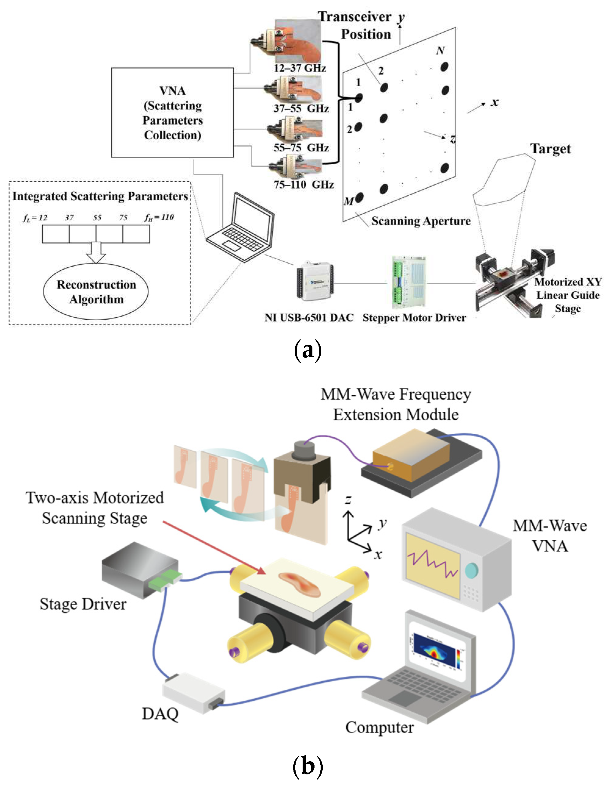
8]. As shown in
Figure 1 (a), this approach involves combining several neighboring imaging sub-bands to create an ultra-wide imaging bandwidth. Each sub-band contains an antenna that operates only within that specific sub-band. These sub-band antennas are placed in front of the target over the scanning aperture, transmit their signals, and record the backscattered responses. The response signals are then integrated using a signal integration algorithm to synthesize an integrated, ultra-wideband signal.
In a separate investigation, we created an imaging system that boasts a remarkably wide bandwidth of 98 GHz through the use of the synthetic ultra-wideband millimeter-wave imaging approach [
9], [
10]. The system design, which merges four adjacent sub-bands to form an ultra-wideband signal, is shown in
Figure 1(b). A measurement platform that can scan tissues across a rectangular aperture plane was created to automate the process. An innovative imaging algorithm was also developed to process the signals and create an image of cancerous tissue in the frequency domain. The image is formed using a reflectivity function, which is the ratio of the reflected to incident fields.
Although the ex-vivo imaging setup was sufficient for initial experiments, it was not practical for in-vivo imaging due to the lengthy measurement time. To address this issue, the number of sub-band antennas was reduced to two, allowing for a much faster imaging process of less than 20 seconds. This led to the development of a real-time imaging system for in-vivo skin cancer diagnosis [
11]. The system was tested on 136 benign and malignant skin lesions from 71 patients, with lesions classified using a 3D principal component analysis and five different classifiers. The results showed that the best classification was achieved with five PCA components followed by multilayer perception, with a sensitivity of 97% and specificity of 98% [
11]. These findings demonstrate that real-time millimeter-wave imaging can accurately distinguish between malignant and benign skin lesions, making it a promising diagnostic tool. The Institutional Review Board (IRB) at the Research Integrity Office of Hackensack University Medical Center (Hackensack, NJ, USA; Protocol# Pro2019-0219) approved this research. The imaging procedures and experimental protocols were conducted in accordance with the guidelines of the Hackensack University Medical Center’s Institutional Review Board (IRB). Before taking measurements, each patient provided written informed consent [
11].
2. Problem Statement
Imaging and communication systems can leverage the wide bandwidths available at millimeter-wave frequencies to achieve high-resolution imaging and high-speed communication [
12]. Over the past decade, several groups have reported silicon-based millimeter-wave imaging systems for biomedical applications with the goal of achieving high resolutions, large image ranges, and short acquisition times [
13], [
14]. However, prior to this work, there existed no imaging chip in the literature with the capability of providing sufficient resolutions for the visualization of biological tissues. In wideband imaging applications, the resolution is directly proportional to the system bandwidth [
15]. It has been suggested that an ultra-wideband millimeter-wave imaging bandwidth of approximately 100 GHz is needed for attaining sufficient resolutions in images of the human skin tissue [
15].
In [
16], we presented three integrated pulse generators that can collectively provide a synthetic ultra-wide imaging bandwidth of 100 GHz in the millimeter-wave regime. The pulse generators produce pulses with frequency ranges of 10–40 GHz, 40–75 GHz, and 75–110 GHz. By this development, a fully integrated ultra-high-resolution imaging chip can be developed using the synthetic ultra-wideband millimeter-wave imaging method. In this work, we design a transceiver front-end that employs the mentioned imaging approach towards the realization of a fully integrated ultra-high-resolution imaging chip for biomedical applications. We realized an ultra-wide imaging bandwidth of 100 GHz by the integration of two adjacent, disjointed frequency sub-bands of 10–50 GHz and 50–110 GHz respectively. The imaging elements were designed and fabricated in a Global Foundry 130-nm SiGe BiCMOS process technology.
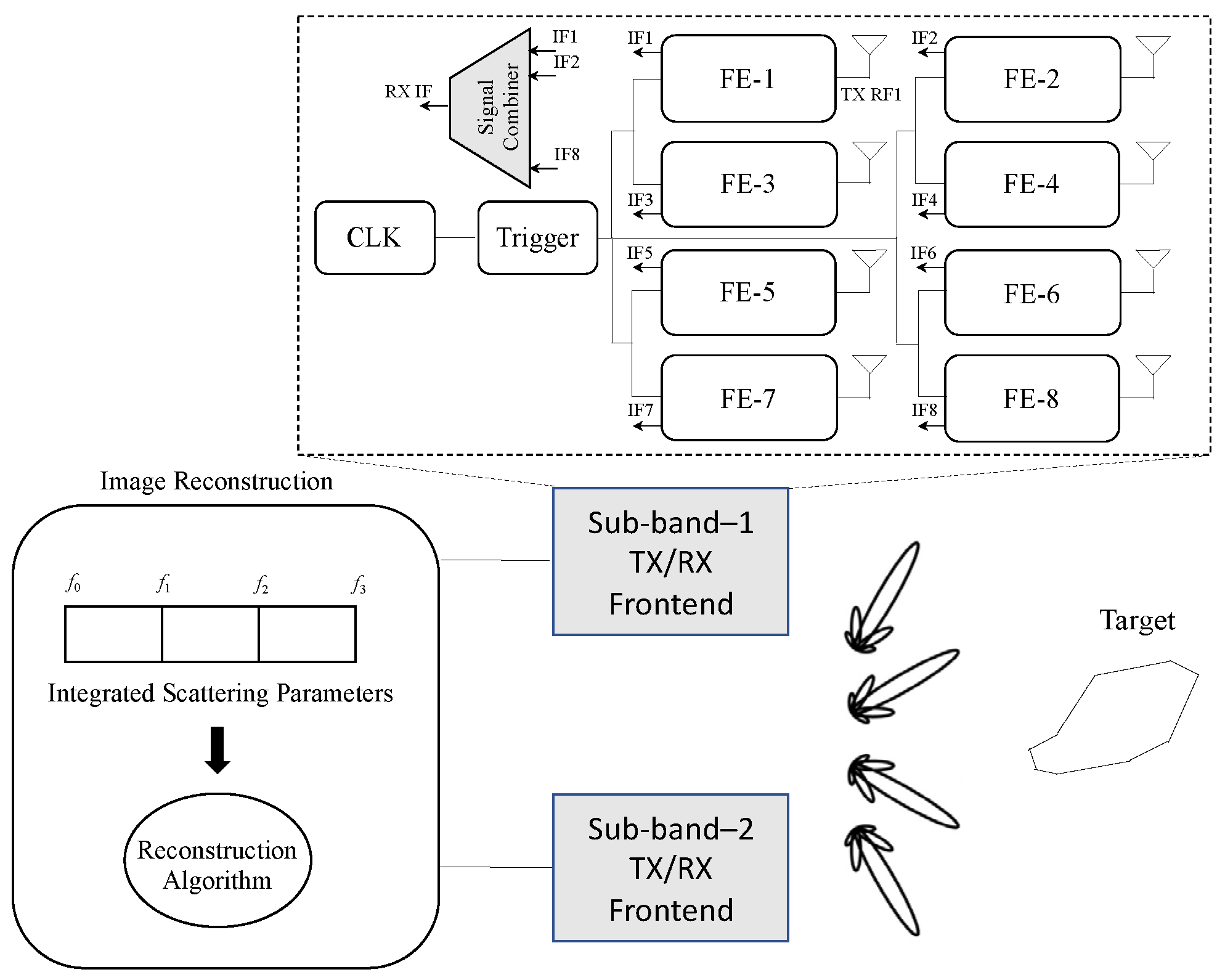
The synthetic ultra-wideband imaging chip is schematically shown in
Figure 2. As seen in this image, each sub-band includes a separate imaging transceiver which operates only within that specific sub-band. Using the transceivers with the embedded phased-array capability, the sub-band antenna beams can be electronically steered to scan the entire region of interest. The received IF signals are filtered and delivered to the image reconstruction module. In this module, an integrated signal is synthesized over the entire bandwidth and a 3D image is formed.
The inset of
Figure 2 displays the schematic of each sub-band transceiver, consisting of 4×2 elements. Each element includes a programmable delay line which controls the radiation timings for coherent combination of the broadband pulses. On-chip antennas are used to eliminate the power loss and phase distortion caused by connections to off-chip antennas. In addition, each antenna is used for both radiation/reception of the waves towards/from the target, respectively. The following sections provide a discussion on the system architecture, the design details of the key building blocks of the front-end, including the pulse generator, multiplier, low-noise amplifier (LNA), transmit/receive (T/R) switch, and on-chip antennas. We then present the characterization results of the simulated and fabricated chips.
3. System Design
The synthetic-aperture radar (SAR) method is commonly used for creating three-dimensional (3D) reconstructions of objects in millimeter-wave imaging studies. However, scanning over a 2D aperture plane increases the size of the system and is not practical for silicon-based systems. In this study, electronic beamforming is used to scan the target region instead. The use of beamforming and beam-steering capabilities improves the range and signal-to-noise ratio (SNR) of the system.
The transceiver front-end is designed for both transmit and receive operations shown in
Figure 2. This is a crucial component for a system that can be expanded by repeating a single unit cell in both the X and Y directions.
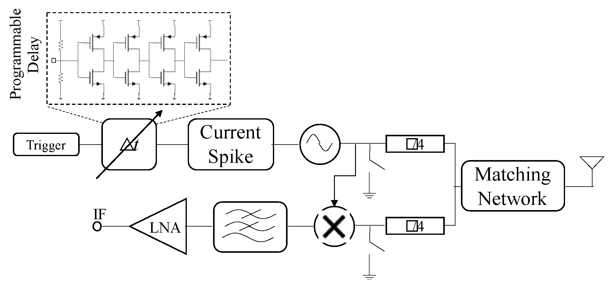
Figure 3 shows the front-end schematic of an array element. The front-end consists of key building blocks, including a pulse generator, a multiplier, an LNA, a T/R switch, and an on-chip antenna in silicon. Separate circuits need to be designed for each component corresponding to the two frequency sub-bands of 10-50 GHz and 50-110 GHz.
In this work, a pulse-radiating approach is adopted because it provides a wider relative bandwidth and higher image resolution compared to continuous-wave radiators [
17]. A delay generator is used to control the timing of the digital signal based on the supply voltage. As demonstrated in
Figure 3, the digital trigger is passed through a programmable delay generator, which is a series of inverter stages that control the timing of the digital signal based on the supply voltage. In transmit mode, the pulse generated by the pulse generator is delayed and transmitted through an antenna, while in receive mode, the front-end receives the backscattered signal, which is mixed with the delayed version of the pulse.
The design of each of the key building blocks is described in the following sections.
3.1. Pulse Generator
The pulse generators designed in this work adopt a pulsed-VCO-based system architecture inspired by our previous work [
16]. The pulse generators convert the input signal to generated pulses with accurate timing, which is required for coherent pulse combining. An asymmetric cross-coupled topology is used to minimize the timing jitter of the radiated pulses and achieve a coherent combination. This results in a significant reduction in power consumption, system complexity, and die area. The pulse generators are designed to produce pulses with full-width-at-half-maximums (FWHM) of 14 ps and 10 ps for the two sub-bands of 10–50 and 50–110 GHz, respectively.
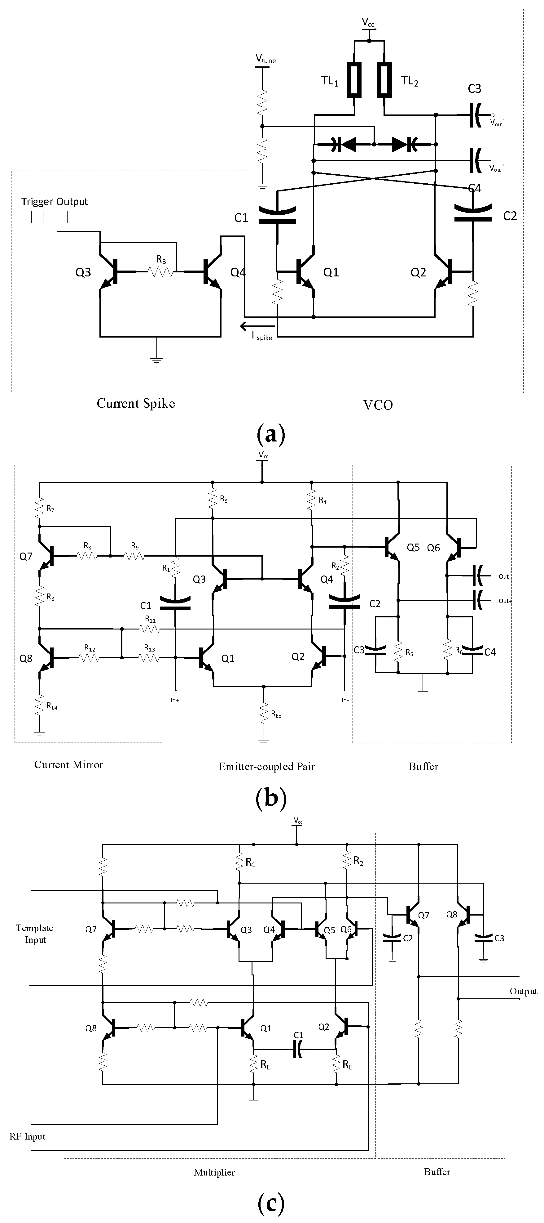
Figure 4 (a) shows the complete schematic of the pulse generator, consisting of a current spike and an asymmetric cross-coupled pulsed VCO topology. When the spike current is high enough to create a negative resistance at the collector terminals of Q1 and Q2, the VCO is turned on. A Schmitt trigger feeds the current spike circuit.
3.2. On-Chip Antenna
To reduce feedline radiation, a broadband slot differential antenna is created that utilizes two signals with equal amplitudes and opposite phases. When designing on-chip millimeter-wave antennas, surface waves can be a concern as they can reduce antenna radiation efficiency. One solution is to use a silicon lens [
18], but this would limit the antenna’s field-of-view. Another solution is to optimize the thickness of the silicon substrate to increase radiation efficiency, and the on-chip antennas are designed to radiate through the substrate due to the potential impact of wire bonds on topside radiation. Because of space limitations, the on-chip antennas are restricted to a maximum dimension of 100 µm. ANSYS HFSS, an electromagnetic simulator, is employed to simulate and optimize the on-chip antennas.
3.3. Low-Noise Amplifier
We use a fully differential structure for the two sub-band low-noise amplifiers. The designed LNAs are based on cascoded emitter-coupled pair design with resistive feedback [
19]. They will have small die areas by avoiding large on-chip spiral inductors.
Figure 4 (b) shows the schematic of the LNA, consisting of an emitter-coupled pair with cascoded devices followed by two emitter-follower stages as buffers [
19]. A current mirror is used to bias the cascode stage. The input and output are differential as the LNA will be connected to the slot bowtie antenna and feed a Gilbert cell-type analog multiplier directly without an unbalanced circuit. The symmetry of the emitter-coupled pair is achieved by placing identical transistors and passive components in the two branches.
3.4. Mixer
Figure 4 (c) shows the schematic of the broadband analog correlator. At the core of the mixer, a Gilbert-cell topology comprising two differential stages in parallel with a cross-coupled output is complemented with a low-pass filter and a differential output buffer. The Gilbert cell acts similar to a wide-band, four-quadrant true multiplier with a proper template pulse amplitude applied to the switching quad. Biasing of the Gilbert-cell multiplier is accomplished with a stacked current mirror. The combination of C1 with
RE forms a capacitively-hunted resistive emitter degeneration, compensating the gain roll-off at high frequencies, which in turn results in a necessary gain and group delay flatness over the targeted frequency band. The low-pass filters are formed by the load resistors of the Gilbert-cell (R1, R2) together with the shunt capacitors (C2, C3) of the buffers. They are used to detect the envelope of the multiplied signals. The highest average power consumption of the sub-band correlators is 30 mW.
4. Simulation Results
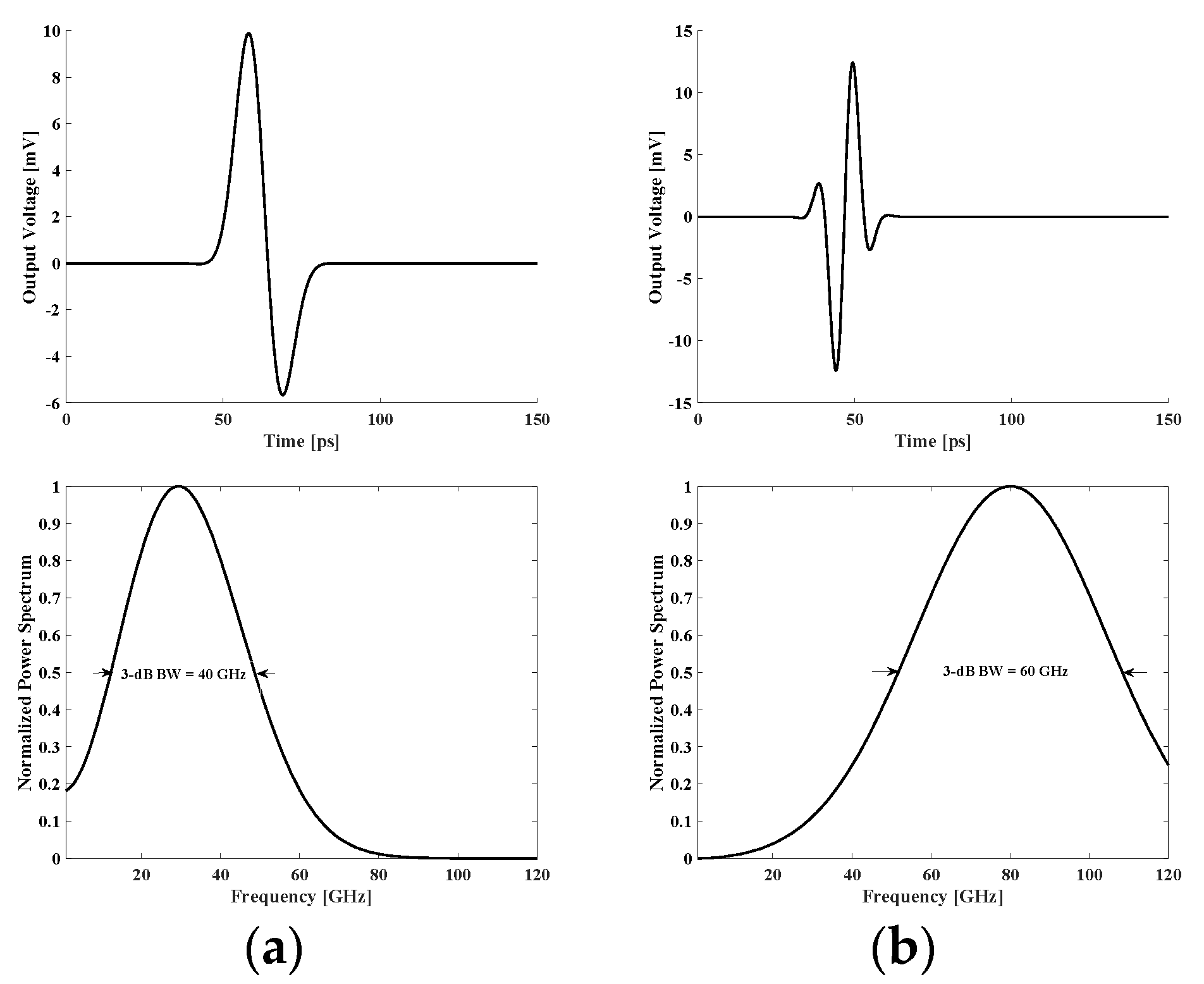
Figure 5 (top) shows the simulated pulses generated by the two sub-band pulse generators. The normalized power spectrums are demonstrated in the bottom row of
Figure 5. The simulated center frequencies are close to the desired values (25 GHz and 80 GHz respectively) and the 3-dB bandwidths are approximately 40 GHz and 60 GHz respectively.
The simulated performance of the sub-band LNAs as stand-alone breakouts is shown in
Figure 6. In the transceiver front-end, the switch output drives the LNA input matching network (
Figure 3). Therefore, the LNA input-matching network is designed for the switch output rather than for a resistance of 50 Ω. The simulated return loss (referred to 50 Ω) is higher than 10 dB. This is due to the different impedance that the LNA input in the breakout sees compared to the actual case with the switch present.
To demonstrate the suitability of the transceiver for imaging applications, a pulse train with 2 GHz repetition rate was fed into the transceiver corresponding to the first sub-band (10–50 GHz). The simulated pulse train can be seen in
Figure 7 (a). The received signal is shown in
Figure 7 (b). The responses of the antenna and the channel are included in the received signal. To characterize the correlation performance, the output of the receiver section is connected to an active low-pass filter with a 3-dB corner frequency of 20 KHz. The simulated cross-correlation of the received pulses with the template pulses is given in
Figure 7 (c). A key constraint of the proposed tiled sub-band front-end approach is the limitation of the front-end size. All sub-band front ends must be integrated in an area smaller than 1.5 mm by 1.5 mm to ensure the spacing of 1.6 mm (~
λ/2) between sub-band front ends while allowing sufficient area for signal combination and distribution among the tiles. The compact imaging front-end designed in this work enables scalable arrays with inter-element spacing by providing dual transmit and receive capability.
The preliminary results of the design are described in our paper [
20].
5. Fabrication
The imaging chip was fabricated in a 130-nm SiGe BiCMOS (8XP) process technology (
fT/
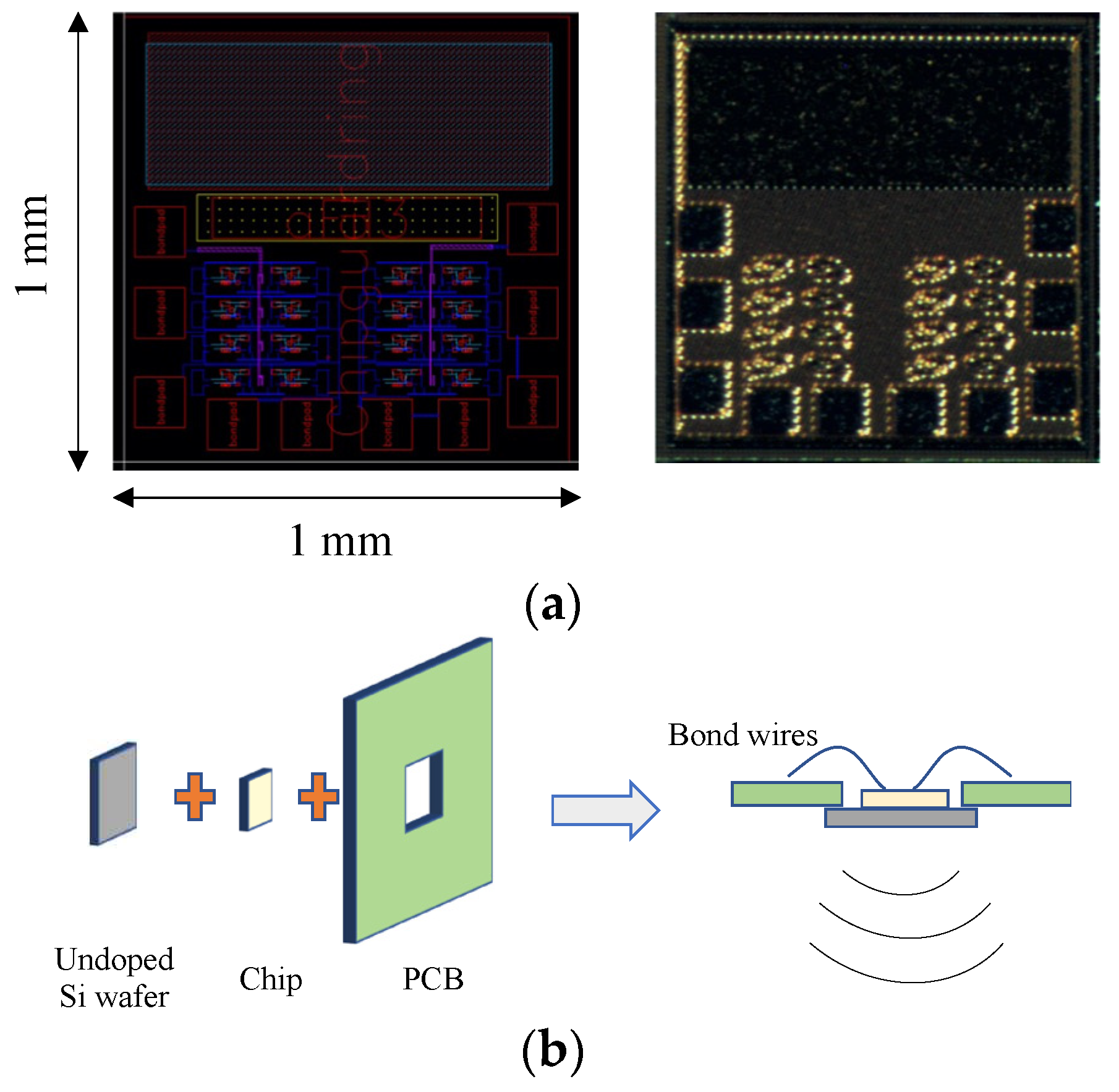
fmax = 200/265 GHz). A micrograph of the chip, which occupies 1 mm × 1 mm die area, is shown in
Figure 8 (a). The fabricated chip is mounted on a piece of undoped silicon slab that is glued to the backside of a Roger 4350B PCB, which has a cut-out, to couple the radiation from the chip substrate to air. Gold wirebonds are used to connect the on-chip pads to PCB traces as shown in
Figure 8 (b).
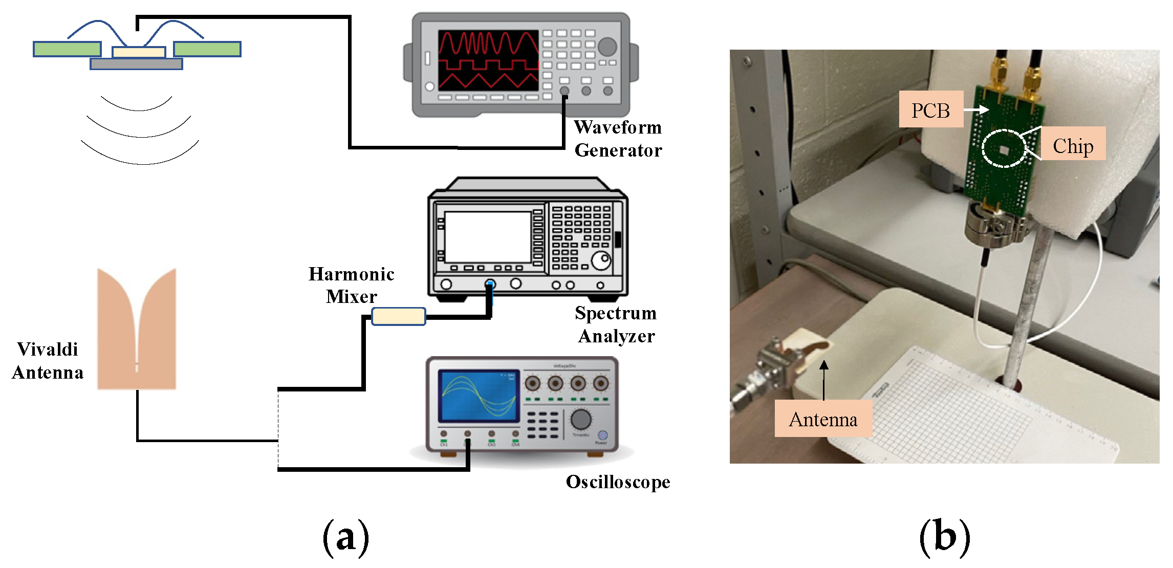
The imager chip is characterized in both time and frequency domains as demonstrated in
Figure 9 (a) and
Figure 9 (b), respectively. The trigger signal is generated by a pulse generator. An SIW-based Vivaldi antenna that we had previously developed [
21] was used as a receiving antenna. A harmonic mixer was used to down convert the high frequency components of the received signal to lower frequencies at which the spectrum analyzer operates. Due to the limited frequency range of the harmonic mixer (75–110 GHz), the frequency-domain characterization was only performed for the second sub-band (50–110 GHz).
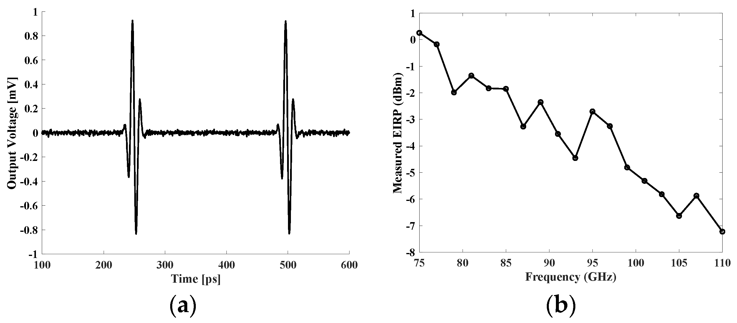
Figure 10 (a) presents the measured pulse waveform for the second sub-band with a FWHM pulse width of 13 ps. Its average equivalent isotropically radiated power (EIRP) frequency spectrum is demonstrated in
Figure 10 (b). As shown in this figure, the radiated pulse has an average EIRP of 0.3 dBm at the center frequency of 75 GHz with a 5-dB bandwidth of nearly 50 GHz. Since the radiated pulse train has a duty-cycle of nearly 25%, the peak EIRP can be estimated to be 4 times larger (6 dB larger) than the measured average EIRP, equaling 6.4 dBm. The difference between the measured and simulated center frequencies (75 GHz and 80 GHz respectively) arises from the effects of the package PCB, variations of the additional silicon slab thickness, and process variations. The chip consumes an average dc power of 194 mW.
The above-mentioned characterizations validate that the proposed imaging chip is capable of transmitting and receiving ultra-wideband signals at millimeter-wave frequencies with low power consumption and high precision. Further evaluation will include radiation pattern measurements to evaluate the beam steering resolution performance.
6. Conclusion and Future Plans
In this work, we built upon our previous work in [
16] and designed a transceiver front-end that employs the synthetic ultra-wideband millimeter-wave imaging approach towards the realization of a fully integrated ultra-high-resolution imaging chip for biomedical applications. We realized an ultra-wide imaging bandwidth of 100 GHz by the integration of two adjacent, disjointed frequency sub-bands of 10–50, 50–110 GHz respectively. The imaging elements were designed and fabricated in a Global Foundry 130-nm SiGe BiCMOS process technology. As discussed in
Section 1, the imaging chip developed in this work promotes a dual-mode operation of receivers and transmitters. This provides greater repeatability, improved system power consumption and system integration. There are, however, a few characteristics of the designed imaging chip, specifically on the on-chip antennas side, that will be improved in the future for having a more efficient imager. Several on-chip antenna structures were studied in the literature to improve their performance in the face of potential challenges in the chip environment [
23,
24,
25,
26]. These will be evaluated and the best solution for our application will be selected.
In the future, we aim to assemble a prototype handheld imager comprising the imaging chip developed in this work. The imager will also include a digital signal processor (DSP) to measure, control, and process continuous signals in the frontend module. The DSP will also execute the image reconstruction algorithm.
Figure 11 shows the rendered image of the compact, handheld imaging device we envision. A display connected to the handheld housing and the processor, a switch connected to the processor, and a rechargeable power source connected to the handheld housing are also other components of the device.
Data availability statements: The datasets used and/or analyzed during the current study are available from the corresponding author on reasonable request.
References
- D. M. Sheen, D. L. McMakin, and T. E. Hall, “Three-dimensional millimeter-wave imaging for concealed weapon detection. IEEE Trans. Microw. Theory Tech. 2001, 49, 1581–1592. [CrossRef]
- D. M. Sheen et al., Wide-bandwidth, wide-beamwidth, high-resolution, millimeter-wave imaging for concealed weapon detection, Proc. SPIE. 2013, 8715, 871509.
- L-3 Communications Security & Detection Systems, Inc, (2018), ProVision2® Imaging [Online]. Available online: https://www.sds.l3t.com/advancedimaging/provision-2.htm.
- R. Appleby and R. N. Anderton, “Millimeter-wave and submillimeter-wave imaging for security and surveillance,” Proc. IEEE. 2007, 95, 1683–1690.
- S. Shrestha, S. Kharkovsky, R. Zoughi, and F. Hepburn, “Microwave and millimeter wave nondestructive evaluation of the space shuttle external tank insulating foam,” Materials Eval. 2005, 63, 339–344.
- M. T. Ghasr et al., “Millimeter wave differential probe for nondestructive detection of corrosion precursor pitting,” IEEE Trans. Instrum. Meas. 2006, 55, 1620–1627.
- Mirbeik-Sabzevari, R. Ashinoff, N. Tavassolian, Ultra-wideband millimeter-wave dielectric properties of freshly-excised normal and malignant human skin tissues. IEEE Trans. Biomed. Eng. 2018, 65, 1320–1329. [Google Scholar] [CrossRef] [PubMed]
- Mirbeik-Sabzevari, S. Li, E. Garay, H. Nguyen, H. Wang, N. Tavassolian, “Synthetic ultra-high-resolution millimeter-wave imaging for skin cancer detection,” IEEE Trans. Biomed. Eng. 2019, 66, 61–71.
- Mirbeik-Sabzevari, R. Ashinoff, and N. Tavassolian, “High-contrast, low-cost, 3D visualization of skin cancer using ultra-high-resolution millimeter-wave imaging,” IEEE Transactions on Medical Imaging 2019, 38, 2188–2197.
- Mirbeik-Sabzevari, R. Ashinoff, and N. Tavassolian “Ultra-high-resolution millimeter-wave imaging: A new promising skin cancer imaging modality,” IEEE Biomedical Circuits and Systems (BioCAS) Conference, Cleveland, OH, 18, pp. 1–4. 20 October.
- Mirbeik, R. Ashinoff, T. Jong et al., “Real-time high-resolution millimeter-wave imaging for in-vivo skin cancer diagnosis,” Sci Rep. 2022, 12, 4971.
- H. B. Wallace, “An application of Advanced SiGe to millimeter-wave phased arrays,” Proc. IEEE MTT-S Int. Microw. Symp. Dig., Jun. 2012, pp. 1–3.
- P. Chen and A. Babakhani, “A 30 GHz impulse radiator with on-chip antennas for high-resolution 3D imaging,” Proc. IEEE Radio Wireless Symp. (RWS), Jan. 2015, pp. 32–34.
- Arbabian, S. Callender, S. Kang, M. Rangwala, and A. M. Niknejad, “A 94 GHz mm-wave-to-baseband pulsed-radar transceiver with applications in imaging and gesture recognition,” IEEE J. Solid-State Circuits. 2013, 48, 1055–1071.
- Mirbeik-Sabzevari and N. Tavassolian, “Tumor Detection Using Millimeter-Wave Technology: Differentiating Between Benign Lesions and Cancer Tissues,” IEEE Microwave Magazine. 2019, 20, 30–43.
- Mirbeik-Sabzevari, L. Najafizadeh and N. Tavassolian, “Synthetic Ultra-Wideband Integrated Pulse Generator for Millimeter-Wave Imaging Applications,” 2020 18th IEEE International New Circuits and Systems Conference (NEWCAS), Montréal, QC, Canada, 2020, pp. 154–157.
- M. Caruso, M. M. Caruso, M. Bassi, A. Bevilacqua and A. Neviani, “A 2-to-16GHz 204mW 3mm-resolution stepped-frequency radar for breast-cancer diagnostic imaging in 65nm CMOS," IEEE International Solid-State Circuits Conference Digest of Technical Papers, San Francisco, CA, USA, 2013.
- R. Han and E. Afshari, “A CMOS high-power broadband 260-GHz radiator array for spectroscopy,” IEEE J. Solid-State Circuits. 2013, 48, 3090–3104.
- D. Lin, B. Schleicher, A. Trasser, and H. Schumacher, “A highly compact SiGe HBT differential LNA for 3.1–10.6 GHz ultra-wideband applications," IEEE International Conference on Ultra-Wideband. 2010, 1, 1–4.
- Mirbeik, L. Najafizadeh, N. Tavassolian, “Synthetic Ultra-Wideband Phased-Array Transceiver for Millimeter-Wave Imaging Applications With On-Chip Antennas,” IEEE International Symposium on Antennas and Propagation (APS/URSI). 2021, 521.
- Mirbeik-Sabzevari, S. Li, E. Garay, H. Nguyen, H. Wang and N. Tavassolian, "W -Band Micromachined Antipodal Vivaldi Antenna Using SIW and CPW Structures," IEEE Transactions on Antennas and Propagation. 2018, 66, 6352–6357.
- H. M. Cheema and A. Shamim, “The last barrier: On-chip antennas,” IEEE Microw. Mag. 2013, 14, 79–91.
- K. Kim et al., ``On-chip antennas in silicon ICs and their application,'' IEEE Trans. Electron Devices. 2005, 52, 1312–1323.
- A. Floyd, C.-M. A. Floyd, C.-M. Hung, and K. O. Kenneth, ``A 15-GHz wireless interconnect implemented in a 0.18- m CMOS technology using integrated transmitters, receivers, and antennas,'' in Symp. VLSI Circuits. Dig. Tech. Papers 2001, 155–158. [Google Scholar]
- Barakat, A. Allam, R. K. Pokharel, H. Elsadek, M. El-Sayed, and K. Yoshida, ``Performance optimization of a 60 GHz antennaon- chip over an arti cial magnetic conductor,'' in Proc. Japan- Egypt Conf. Electron., Commun. Comput. (JEC-ECC), 2012, 118–121.
- F. Gutierrez, Jr., K. F. Gutierrez, Jr., K. Parrish, and T. S. Rappaport, ``On-chip integrated antenna structures in CMOS for 60 GHz WPAN systems,'' in Proc. IEEE Global Telecommun. Conf. (GLOBECOM), Nov. 2009, pp. 1–7.
|
Disclaimer/Publisher’s Note: The statements, opinions and data contained in all publications are solely those of the individual author(s) and contributor(s) and not of MDPI and/or the editor(s). MDPI and/or the editor(s) disclaim responsibility for any injury to people or property resulting from any ideas, methods, instructions or products referred to in the content. |
© 2023 by the authors. Licensee MDPI, Basel, Switzerland. This article is an open access article distributed under the terms and conditions of the Creative Commons Attribution (CC BY) license (http://creativecommons.org/licenses/by/4.0/).
