Submitted:
12 October 2023
Posted:
13 October 2023
You are already at the latest version
Abstract
Keywords:
I. INTRODUCTION
II. DEVICE FABRICATION AND CHARACTERISATION
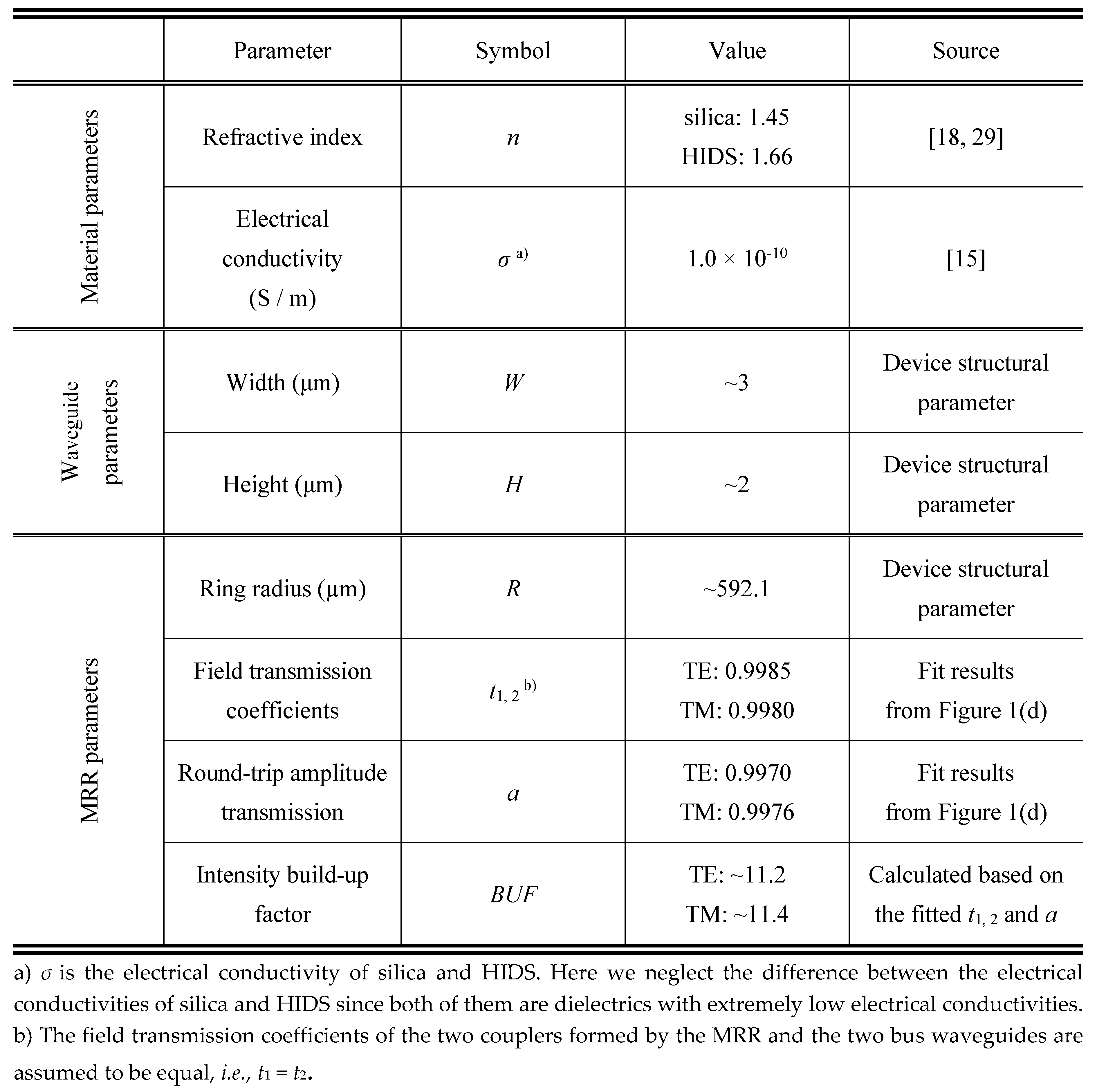
III. THERMO-OPTIC COEFFICIENT
IV. OPTICALLY INDUCED THERMO-OPTIC RESPONSE
V. OPTICAL BISTABILITY
VI. THERMAL CONDUCTIVITY
VII. COMPARISON WITH OTHER INTEGRATED PLATFORM MATERIALS
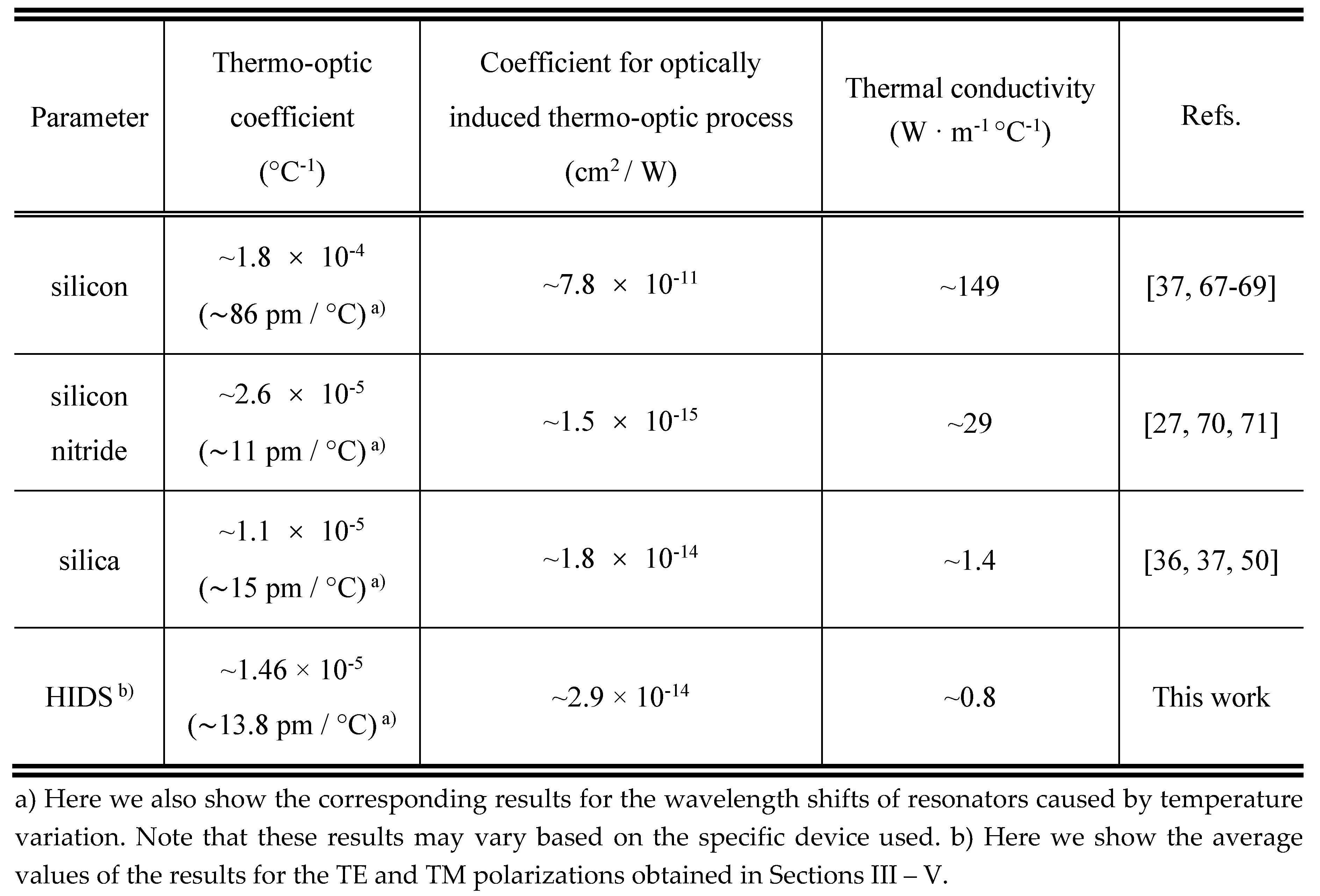
VIII. CONCLUSION
References
- Y. Li, W. Li, T. Han, X. Zheng, J. Li, B. Li, S. Fan, and C.-W. Qiu, “Transforming heat transfer with thermal metamaterials and devices,” Nature Reviews Materials, vol. 6, no. 6, pp. 488-507, 2021. [CrossRef]
- H. Zhu, Q. Li, C. Zheng, Y. Hong, Z. Xu, H. Wang, W. Shen, S. Kaur, P. Ghosh, and M. Qiu, “High-temperature infrared camouflage with efficient thermal management,” Light: Science & Applications, vol. 9, no. 1, pp. 60, 2020/04/14, 2020. [CrossRef]
- C. Wang, M. Zhang, X. Chen, M. Bertrand, A. Shams-Ansari, S. Chandrasekhar, P. Winzer, and M. Lončar, “Integrated lithium niobate electro-optic modulators operating at CMOS-compatible voltages,” Nature, vol. 562, no. 7725, pp. 101-104, 2018/10/01, 2018. [CrossRef]
- K. Wu, Y. Wang, C. Qiu, and J. Chen, “Thermo-optic all-optical devices based on two-dimensional materials,” Photonics Research, vol. 6, no. 10, pp. C22-C28, 2018/10/01, 2018. [CrossRef]
- B. Desiatov, I. Goykhman, and U. Levy, “Direct Temperature Mapping of Nanoscale Plasmonic Devices,” Nano Letters, vol. 14, no. 2, pp. 648-652, 2014/02/12, 2014. [CrossRef]
- Q. Huang, H. Yu, Q. Zhang, Y. Li, W. Chen, Y. Wang, and J. Yang, “Thermally enhanced responsivity in an all-silicon optical power monitor based on defect-mediated absorption,” Photonics Research, vol. 9, no. 11, pp. 2205, 2021. [CrossRef]
- Y. Sun, J. Wu, M. Tan, X. Xu, Y. Li, R. Morandotti, A. Mitchell, and D. J. Moss, “Applications of optical microcombs,” Advances in Optics and Photonics, vol. 15, no. 1, pp. 86, 2023. [CrossRef]
- T. Herr, V. Brasch, J. D. Jost, C. Y. Wang, N. M. Kondratiev, M. L. Gorodetsky, and T. J. Kippenberg, “Temporal solitons in optical microresonators,” Nature Photonics, vol. 8, no. 2, pp. 145-152, 2014/02/01, 2014. [CrossRef]
- C. Qiu, C. Zhang, H. Zeng, and T. Guo, “High-Performance Graphene-on-Silicon Nitride All-Optical Switch Based on a Mach–Zehnder Interferometer,” Journal of Lightwave Technology, vol. 39, no. 7, pp. 2099-2105, 2021. [CrossRef]
- C. Qiu, Y. Yang, C. Li, Y. Wang, K. Wu, and J. Chen, “All-optical control of light on a graphene-on-silicon nitride chip using thermo-optic effect,” Scientific Reports, vol. 7, no. 1, pp. 17046, 2017/12/06, 2017. [CrossRef]
- P. W. Smith, and W. J. Tomlinson, “Bistable optical devices promise subpicosecond switching,” IEEE Spectrum, vol. 18, pp. 26-33, June 01, 1981, 1981.
- M. Shirdel, and M. A. Mansouri-Birjandi, “All-optical bistable switching, hard-limiter and wavelength-controlled power source,” Frontiers of Optoelectronics, vol. 9, no. 4, pp. 560-564, 2016/12/01, 2016. [CrossRef]
- H. Gibbs, “Optical Bistability: Controlling Light with Light, Academic Press,” Inc.: Orlando, FL, USA, 1985.
- V. R. Almeida, and M. Lipson, “Optical bistability on a silicon chip,” Optics Letters, vol. 29, no. 20, pp. 2387-2389, 2004/10/15, 2004. [CrossRef]
- M. Ferrera, L. Razzari, D. Duchesne, R. Morandotti, Z. Yang, M. Liscidini, J. E. Sipe, S. Chu, B. E. Little, and D. J. Moss, “Low-power continuous-wave nonlinear optics in doped silica glass integrated waveguide structures,” Nature Photonics, vol. 2, no. 12, pp. 737-740, 2008. [CrossRef]
- M. Ferrera, Y. Park, L. Razzari, B. E. Little, S. T. Chu, R. Morandotti, D. J. Moss, and J. Azaña, “On-chip CMOS-compatible all-optical integrator,” Nature Communications, vol. 1, no. 1, pp. 29, 2010/06/15, 2010. [CrossRef]
- L. Razzari, D. Duchesne, M. Ferrera, R. Morandotti, S. Chu, B. E. Little, and D. J. Moss, “CMOS-compatible integrated optical hyper-parametric oscillator,” Nature Photonics, vol. 4, no. 1, pp. 41-45, 2010/01/01, 2010. [CrossRef]
- D. J. Moss, R. Morandotti, A. L. Gaeta, and M. Lipson, “New CMOS-compatible platforms based on silicon nitride and Hydex for nonlinear optics,” Nature Photonics, vol. 7, no. 8, pp. 597-607, 2013. [CrossRef]
- H. Bao, A. Cooper, M. Rowley, L. Di Lauro, J. S. Totero Gongora, S. T. Chu, B. E. Little, G.-L. Oppo, R. Morandotti, D. J. Moss, B. Wetzel, M. Peccianti, and A. Pasquazi, “Laser cavity-soliton microcombs,” Nature Photonics, vol. 13, no. 6, pp. 384-389, 2019. [CrossRef]
- M. Kues, C. Reimer, P. Roztocki, L. R. Cortés, S. Sciara, B. Wetzel, Y. Zhang, A. Cino, S. T. Chu, B. E. Little, D. J. Moss, L. Caspani, J. Azaña, and R. Morandotti, “On-chip generation of high-dimensional entangled quantum states and their coherent control,” Nature, vol. 546, no. 7660, pp. 622-626, 2017/06/01, 2017. [CrossRef]
- C. Reimer, M. Kues, P. Roztocki, B. Wetzel, F. Grazioso, B. E. Little, S. T. Chu, T. Johnston, Y. Bromberg, L. Caspani, D. J. Moss, and R. Morandotti, “Generation of multiphoton entangled quantum states by means of integrated frequency combs,” Science, vol. 351, no. 6278, pp. 1176-1180, 2016. [CrossRef]
- M. Rowley, P.-H. Hanzard, A. Cutrona, H. Bao, S. T. Chu, B. E. Little, R. Morandotti, D. J. Moss, G.-L. Oppo, J. S. Totero Gongora, M. Peccianti, and A. Pasquazi, “Self-emergence of robust solitons in a microcavity,” Nature, vol. 608, no. 7922, pp. 303-309, 2022/08/01, 2022. [CrossRef]
- X. Xu, M. Tan, B. Corcoran, J. Wu, A. Boes, T. G. Nguyen, S. T. Chu, B. E. Little, D. G. Hicks, R. Morandotti, A. Mitchell, and D. J. Moss, “11 TOPS photonic convolutional accelerator for optical neural networks,” Nature, vol. 589, no. 7840, pp. 44-51, 2021. [CrossRef]
- B. Corcoran, M. Tan, X. Xu, A. Boes, J. Wu, T. G. Nguyen, S. T. Chu, B. E. Little, R. Morandotti, A. Mitchell, and D. J. Moss, “Ultra-dense optical data transmission over standard fibre with a single chip source,” Nature Communications, vol. 11, no. 1, pp. 2568, 2020/05/22, 2020. [CrossRef]
- J. Wu, Y. Yang, Y. Qu, X. Xu, Y. Liang, S. T. Chu, B. E. Little, R. Morandotti, B. Jia, and D. J. Moss, “Graphene Oxide Waveguide and Micro-Ring Resonator Polarizers,” Laser & Photonics Reviews, vol. 13, no. 9, pp. 1900056, 2019/09/01, 2019. [CrossRef]
- J. Wu, Y. Yang, Y. Qu, L. Jia, Y. Zhang, X. Xu, S. T. Chu, B. E. Little, R. Morandotti, B. Jia, and D. J. Moss, “2D Layered Graphene Oxide Films Integrated with Micro-Ring Resonators for Enhanced Nonlinear Optics,” Small, vol. 16, no. 16, pp. 1906563, 2020/04/01, 2020. [CrossRef]
- Y. Gao, W. Zhou, X. Sun, H. K. Tsang, and C. Shu, “Cavity-enhanced thermo-optic bistability and hysteresis in a graphene-on-Si3N4 ring resonator,” Optics Letters, vol. 42, no. 10, pp. 1950-1953, 2017/05/15, 2017. [CrossRef]
- G. Priem, P. Dumon, W. Bogaerts, D. V. Thourhout, G. Morthier, and R. Baets, “Optical bistability and pulsating behaviour in Silicon-On-Insulator ring resonator structures,” Optics Express, vol. 13, no. 23, pp. 9623-9628, 2005/11/14, 2005. [CrossRef]
- Y. Zhang, J. Wu, L. Jia, Y. Qu, Y. Yang, B. Jia, and D. J. Moss, “Graphene Oxide for Nonlinear Integrated Photonics,” Laser & Photonics Reviews, vol. 17, no. 3, pp. 2200512, 2023/03/01, 2023. [CrossRef]
- H. Arianfard, S. Juodkazis, D. J. Moss, and J. Wu, “Sagnac interference in integrated photonics,” Applied Physics Reviews, vol. 10, no. 1, 2023. [CrossRef]
- J. Wu, P. Cao, T. Pan, Y. Yang, C. Qiu, C. Tremblay, and Y. Su, “Compact on-chip 1 × 2 wavelength selective switch based on silicon microring resonator with nested pairs of subrings,” Photonics Research, vol. 3, no. 1, pp. 9-14, 2015/02/01, 2015. [CrossRef]
- G. Cocorullo, F. G. Della Corte, I. Rendina, and P. M. Sarro, “Thermo-optic effect exploitation in silicon microstructures,” Sensors and Actuators A: Physical, vol. 71, no. 1, pp. 19-26, 1998/11/01/, 1998. [CrossRef]
- A. Grieco, B. Slutsky, D. T. H. Tan, S. Zamek, M. P. Nezhad, and Y. Fainman, “Optical Bistability in a Silicon Waveguide Distributed Bragg Reflector Fabry–Pérot Resonator,” Journal of Lightwave Technology, vol. 30, no. 14, pp. 2352-2355, 2012.
- M. Ferrera, D. Duchesne, L. Razzari, M. Peccianti, R. Morandotti, P. Cheben, S. Janz, D. X. Xu, B. E. Little, S. Chu, and D. J. Moss, “Low power four wave mixing in an integrated, micro-ring resonator with Q = 1.2 million,” Optics Express, vol. 17, no. 16, pp. 14098-14103, 2009/08/03, 2009.
- J. Wu, T. Moein, X. Xu, G. Ren, A. Mitchell, and D. J. Moss, “Micro-ring resonator quality factor enhancement via an integrated Fabry-Perot cavity,” APL Photonics, vol. 2, no. 5, 2017. [CrossRef]
- H. Gao, Y. Jiang, Y. Cui, L. Zhang, J. Jia, and L. Jiang, “Investigation on the Thermo-Optic Coefficient of Silica Fiber Within a Wide Temperature Range,” Journal of Lightwave Technology, vol. 36, no. 24, pp. 5881-5886, 2018. [CrossRef]
- C. Horvath, D. Bachman, R. Indoe, and V. Van, “Photothermal nonlinearity and optical bistability in a graphene–silicon waveguide resonator,” Optics Letters, vol. 38, no. 23, pp. 5036-5039, 2013. [CrossRef]
- M. A. Foster, A. C. Turner, J. E. Sharping, B. S. Schmidt, M. Lipson, and A. L. Gaeta, “Broad-band optical parametric gain on a silicon photonic chip,” Nature, vol. 441, no. 7096, pp. 960-963, 2006/06/01, 2006. [CrossRef]
- J. Leuthold, C. Koos, and W. Freude, “Nonlinear silicon photonics,” Nature Photonics, vol. 4, no. 8, pp. 535-544, 2010. [CrossRef]
- J. Wu, H. Lin, D. J. Moss, K. P. Loh, and B. Jia, “Graphene oxide for photonics, electronics and optoelectronics,” Nature Reviews Chemistry, vol. 7, no. 3, pp. 162-183, 2023/03/01, 2023.
- J. Wu, L. Jia, Y. Zhang, Y. Qu, B. Jia, and D. J. Moss, “Graphene Oxide for Integrated Photonics and Flat Optics,” Advanced Materials, vol. 33, no. 3, pp. 2006415, 2021/01/01, 2021. [CrossRef]
- J. Wu, B. Liu, J. Peng, J. Mao, X. Jiang, C. Qiu, C. Tremblay, and Y. Su, “On-Chip Tunable Second-Order Differential-Equation Solver Based on a Silicon Photonic Mode-Split Microresonator,” Journal of Lightwave Technology, vol. 33, no. 17, pp. 3542-3549, 2015. [CrossRef]
- K. Ikeda, R. E. Saperstein, N. Alic, and Y. Fainman, “Thermal and Kerr nonlinear properties of plasma-deposited silicon nitride/silicon dioxide waveguides,” Optics express, vol. 16, no. 17, pp. 12987-12994, 2008. [CrossRef]
- T. Gu, M. Yu, D.-L. Kwong, and C. W. Wong, “Molecular-absorption-induced thermal bistability in PECVD silicon nitride microring resonators,” Optics Express, vol. 22, no. 15, pp. 18412-18420, 2014/07/28, 2014. [CrossRef]
- L.-W. Luo, G. S. Wiederhecker, K. Preston, and M. Lipson, “Power insensitive silicon microring resonators,” Optics Letters, vol. 37, no. 4, pp. 590-592, 2012/02/15, 2012. [CrossRef]
- Y. Qu, J. Wu, Y. Zhang, L. Jia, Y. Liang, B. Jia, and D. J. Moss, “Analysis of Four-Wave Mixing in Silicon Nitride Waveguides Integrated With 2D Layered Graphene Oxide Films,” Journal of Lightwave Technology, vol. 39, no. 9, pp. 2902-2910, 2021/05/01, 2021. [CrossRef]
- Y. Zhang, J. Wu, Y. Qu, L. Jia, B. Jia, and D. J. Moss, “Design and Optimization of Four-Wave Mixing in Microring Resonators Integrated With 2D Graphene Oxide Films,” Journal of Lightwave Technology, vol. 39, no. 20, pp. 6553-6562, 2021. [CrossRef]
- W. Bogaerts, P. De Heyn, T. Van Vaerenbergh, K. De Vos, S. Kumar Selvaraja, T. Claes, P. Dumon, P. Bienstman, D. Van Thourhout, and R. Baets, “Silicon microring resonators,” Laser & Photonics Reviews, vol. 6, no. 1, pp. 47-73, 2012.
- Y. Yang, J. Wu, X. Xu, Y. Liang, S. T. Chu, B. E. Little, R. Morandotti, B. Jia, and D. J. Moss, “Invited Article: Enhanced four-wave mixing in waveguides integrated with graphene oxide,” APL Photonics, vol. 3, no. 12, pp. 120803, 2018. [CrossRef]
- Q. Ma, T. Rossmann, and Z. Guo, “Temperature sensitivity of silica micro-resonators,” Journal of Physics D: Applied Physics, vol. 41, no. 24, pp. 245111, 2008/12/03, 2008. [CrossRef]
- L. Jin, L. Di Lauro, A. Pasquazi, M. Peccianti, D. J. Moss, R. Morandotti, B. E. Little, and S. T. Chu, “Optical multi-stability in a nonlinear high-order microring resonator filter,” APL Photonics, vol. 5, no. 5, 2020. [CrossRef]
- I.D. Rukhlenko, M. Premaratne, and G. P. Agrawal, “Analytical study of optical bistability in silicon ring resonators,” Optics Letters, vol. 35, no. 1, pp. 55-57, 2010/01/01, 2010. [CrossRef]
- T. Gu, N. Petrone, J. F. McMillan, A. van der Zande, M. Yu, G.-Q. Lo, D.-L. Kwong, J. Hone, and C. W. Wong, “Regenerative oscillation and four-wave mixing in graphene optoelectronics,” Nature photonics, vol. 6, no. 8, pp. 554-559, 2012.
- Y. Zhang, L. Tao, D. Yi, J.-b. Xu, and H. K. Tsang, “Enhanced thermo-optic nonlinearities in a MoS2-on-silicon microring resonator,” Applied Physics Express, vol. 13, no. 2, pp. 022004, 2020. [CrossRef]
- J. Wu, X. Xu, T. G. Nguyen, S. T. Chu, B. E. Little, R. Morandotti, A. Mitchell, and D. J. Moss, “RF Photonics: An Optical Microcombs’ Perspective,” IEEE Journal of Selected Topics in Quantum Electronics, vol. 24, no. 4, pp. 1-20, 2018.
- S. Ghosh, I. Calizo, D. Teweldebrhan, E. P. Pokatilov, D. L. Nika, A. A. Balandin, W. Bao, F. Miao, and C. N. Lau, “Extremely high thermal conductivity of graphene: Prospects for thermal management applications in nanoelectronic circuits,” Applied Physics Letters, vol. 92, no. 15, 2008. [CrossRef]
- P. Goli, S. Legedza, A. Dhar, R. Salgado, J. Renteria, and A. A. Balandin, “Graphene-enhanced hybrid phase change materials for thermal management of Li-ion batteries,” Journal of Power Sources, vol. 248, pp. 37-43, 2014/02/15/, 2014. [CrossRef]
- J. D. Renteria, D. L. Nika, and A. A. Balandin, “Graphene Thermal Properties: Applications in Thermal Management and Energy Storage,” Applied Sciences, 4, 2014]. [CrossRef]
- A. Shakouri, “Nanoscale Thermal Transport and Microrefrigerators on a Chip,” Proceedings of the IEEE, vol. 94, no. 8, pp. 1613-1638, 2006. [CrossRef]
- N. Mehra, L. Mu, T. Ji, X. Yang, J. Kong, J. Gu, and J. Zhu, “Thermal transport in polymeric materials and across composite interfaces,” Applied Materials Today, vol. 12, pp. 92-130, 2018/09/01/, 2018. [CrossRef]
- C. Horvath, D. Bachman, R. Indoe, and V. Van, “Photothermal nonlinearity and optical bistability in a graphene-silicon waveguide resonator,” Optics Letters, vol. 38, no. 23, pp. 5036-5039, 2013/12/01, 2013. [CrossRef]
- B. E. Little, S. T. Chu, P. P. Absil, J. V. Hryniewicz, F. G. Johnson, F. Seiferth, D. Gill, V. Van, O. King, and M. Trakalo, “Very high-order microring resonator filters for WDM applications,” IEEE Photonics Technology Letters, vol. 16, no. 10, pp. 2263-2265, 2004. [CrossRef]
- B. Little, “A VLSI Photonics Platform,” Technical Digest. p. ThD1.
- A. Gyanathan, and Y.-C. Yeo, “Multi-level phase change memory devices with Ge2Sb2Te5 layers separated by a thermal insulating Ta2O5 barrier layer,” Journal of Applied Physics, vol. 110, no. 12, 2011. [CrossRef]
- M. L. Grilli, D. Ristau, M. Dieckmann, and U. Willamowski, “Thermal conductivity of e-beam coatings,” Applied Physics A, vol. 71, no. 1, pp. 71-76, 2000/07/01, 2000. [CrossRef]
- J. V. Campenhout, P. Rojo-Romeo, D. V. Thourhout, C. Seassal, P. Regreny, L. D. Cioccio, J. M. Fedeli, and R. Baets, “Thermal Characterization of Electrically Injected Thin-Film InGaAsP Microdisk Lasers on Si,” Journal of Lightwave Technology, vol. 25, no. 6, pp. 1543-1548, 2007.
- J. Komma, C. Schwarz, G. Hofmann, D. Heinert, and R. Nawrodt, “Thermo-optic coefficient of silicon at 1550 nm and cryogenic temperatures,” Applied Physics Letters, vol. 101, no. 4, 2012.
- G. Cocorullo, F. G. Della Corte, and I. Rendina, “Temperature dependence of the thermo-optic coefficient in crystalline silicon between room temperature and 550 K at the wavelength of 1523 nm,” Applied Physics Letters, vol. 74, no. 22, pp. 3338-3340, 1999.
- W.-C. Hsu, C. Zhen, and A. X. Wang, “Electrically Tunable High-Quality Factor Silicon Microring Resonator Gated by High Mobility Conductive Oxide,” ACS Photonics, vol. 8, no. 7, pp. 1933-1936, 2021/07/21, 2021.
- P. E. Barclay, K. Srinivasan, and O. Painter, “Nonlinear response of silicon photonic crystal microresonators excited via an integrated waveguide and fiber taper,” Optics Express, vol. 13, no. 3, pp. 801-820, 2005/02/07, 2005.
- D. Dai, Z. Wang, J. F. Bauters, M. C. Tien, M. J. R. Heck, D. J. Blumenthal, and J. E. Bowers, “Low-loss Si3N4 arrayed-waveguide grating (de)multiplexer using nano-core optical waveguides,” Optics Express, vol. 19, no. 15, pp. 14130-14136, 2011/07/18, 2011.
- X. Xu, J. Wu, M. Shoeiby, T. G. Nguyen, S. T. Chu, B. E. Little, R. Morandotti, A. Mitchell, and D. J. Moss, “Reconfigurable broadband microwave photonic intensity differentiator based on an integrated optical frequency comb source,” APL Photonics, vol. 2, no. 9, 096104, Sep. 2017.
- Xu, X., et al., Photonic microwave true time delays for phased array antennas using a 49 GHz FSR integrated micro-comb source, Photonics Research, 6, B30-B36 (2018).
- X. Xu, M. Tan, J. Wu, R. Morandotti, A. Mitchell, and D. J. Moss, “Microcomb-based photonic RF signal processing”, IEEE Photonics Technology Letters, vol. 31 no. 23 1854-1857, 2019.
- Xu, et al., “Advanced adaptive photonic RF filters with 80 taps based on an integrated optical micro-comb source,” Journal of Lightwave Technology, vol. 37, no. 4, pp. 1288-1295 (2019).
- X. Xu, et al., “Photonic RF and microwave integrator with soliton crystal microcombs”, IEEE Transactions on Circuits and Systems II: Express Briefs, vol. 67, no. 12, pp. 3582-3586, 2020.
- X. Xu, et al., “High performance RF filters via bandwidth scaling with Kerr micro-combs,” APL Photonics, vol. 4 (2) 026102. 2019.
- M. Tan, et al., “Microwave and RF photonic fractional Hilbert transformer based on a 50 GHz Kerr micro-comb”, Journal of Lightwave Technology, vol. 37, no. 24, pp. 6097 – 6104, 2019.
- M. Tan, et al., “RF and microwave fractional differentiator based on photonics”, IEEE Transactions on Circuits and Systems: Express Briefs, vol. 67, no.11, pp. 2767-2771, 2020.
- M. Tan, et al., “Photonic RF arbitrary waveform generator based on a soliton crystal micro-comb source”, Journal of Lightwave Technology, vol. 38, no. 22, pp. 6221-6226 (2020).
- M. Tan, X. Xu, J. Wu, R. Morandotti, A. Mitchell, and D. J. Moss, “RF and microwave high bandwidth signal processing based on Kerr Micro-combs”, Advances in Physics X, VOL. 6, NO. 1, 1838946 (2021). [CrossRef]
- X. Xu, et al., “Advanced RF and microwave functions based on an integrated optical frequency comb source,” Opt. Express, vol. 26 (3) 2569 (2018).
- M. Tan, X. Xu, J. Wu, B. Corcoran, A. Boes, T. G. Nguyen, S. T. Chu, B. E. Little, R.Morandotti, A. Lowery, A. Mitchell, and D. J. Moss, ““Highly Versatile Broadband RF Photonic Fractional Hilbert Transformer Based on a Kerr Soliton Crystal Microcomb”, Journal of Lightwave Technology vol. 39 (24) 7581-7587 (2021).
- Wu, J. et al. RF Photonics: An Optical Microcombs’ Perspective. IEEE Journal of Selected Topics in Quantum Electronics Vol. 24, 6101020, 1-20 (2018).
- T. G. Nguyen et al., “Integrated frequency comb source-based Hilbert transformer for wideband microwave photonic phase analysis,” Opt. Express, vol. 23, no. 17, pp. 22087-22097, Aug. 2015.
- X. Xu, et al., “Broadband RF channelizer based on an integrated optical frequency Kerr comb source,” Journal of Lightwave Technology, vol. 36, no. 19, pp. 4519-4526, 2018.
- X. Xu, et al., “Continuously tunable orthogonally polarized RF optical single sideband generator based on micro-ring resonators,” Journal of Optics, vol. 20, no. 11, 115701. 2018.
- X. Xu, et al., “Orthogonally polarized RF optical single sideband generation and dual-channel equalization based on an integrated microring resonator,” Journal of Lightwave Technology, vol. 36, no. 20, pp. 4808-4818. 2018.
- X. Xu, et al., “Photonic RF phase-encoded signal generation with a microcomb source”, J. Lightwave Technology, vol. 38, no. 7, 1722-1727, 2020.
- X. Xu, et al., Broadband microwave frequency conversion based on an integrated optical micro-comb source”, Journal of Lightwave Technology, vol. 38 no. 2, pp. 332-338, 2020.
- M. Tan, et al., “Photonic RF and microwave filters based on 49GHz and 200GHz Kerr microcombs”, Optics Comm. vol. 465,125563, Feb. 22. 2020.
- X. Xu, et al., “Broadband photonic RF channelizer with 90 channels based on a soliton crystal microcomb”, Journal of Lightwave Technology, Vol. 38, no. 18, pp. 5116 – 5121 (2020).
- M. Tan et al, “Orthogonally polarized Photonic Radio Frequency single sideband generation with integrated micro-ring resonators”, IOP Journal of Semiconductors, Vol. 42 (4), 041305 (2021).
- Mengxi Tan, X. Xu, J. Wu, T. G. Nguyen, S. T. Chu, B. E. Little, R. Morandotti, A. Mitchell, and David J. Moss, “Photonic Radio Frequency Channelizers based on Kerr Optical Micro-combs”, IOP Journal of Semiconductors Vol. 42 (4), 041302 (2021). DOI:10.1088/1674-4926/42/4/041302.
- B. Corcoran, et al., “Ultra-dense optical data transmission over standard fiber with a single chip source”, Nature Communications, vol. 11, Article:2568, 2020.
- X. Xu et al, “Photonic perceptron based on a Kerr microcomb for scalable high speed optical neural networks”, Laser and Photonics Reviews, vol. 14, no. 8, 2000070 (2020).
- X. Xu, et al., “11 TOPs photonic convolutional accelerator for optical neural networks”, Nature 589, 44-51 (2021).
- X. Xu et al., “Neuromorphic computing based on wavelength-division multiplexing”, 28 IEEE Journal of Selected Topics in Quantum Electronics Vol. 29 Issue: 2, Article 7400112 (2023). [CrossRef]
- Yang Sun, Jiayang Wu, Mengxi Tan, Xingyuan Xu, Yang Li, Roberto Morandotti, Arnan Mitchell, and David Moss, “Applications of optical micro-combs”, Advances in Optics and Photonics 15 (1) 86-175 (2023).
- Yunping Bai, Xingyuan Xu,1, Mengxi Tan, Yang Sun, Yang Li, Jiayang Wu, Roberto Morandotti, Arnan Mitchell, Kun Xu, and David J. Moss, “Photonic multiplexing techniques for neuromorphic computing”, Nanophotonics 12 (5): 795–817 (2023).
- Chawaphon Prayoonyong, Andreas Boes, Xingyuan Xu, Mengxi Tan, Sai T. Chu, Brent E. Little, Roberto Morandotti, Arnan Mitchell, David J. Moss, and Bill Corcoran, “Frequency comb distillation for optical superchannel transmission”, Journal of Lightwave Technology 39 (23) 7383-7392 (2021).
- Mengxi Tan, Xingyuan Xu, Jiayang Wu, Bill Corcoran, Andreas Boes, Thach G. Nguyen, Sai T. Chu, Brent E. Little, Roberto Morandotti, Arnan Mitchell, and David J. Moss, “Integral order photonic RF signal processors based on a soliton crystal micro-comb source”, IOP Journal of Optics 23 (11) 125701 (2021).
- Yang Sun, Jiayang Wu, Yang Li, Xingyuan Xu, Guanghui Ren, Mengxi Tan, Sai Tak Chu, Brent E. Little, Roberto Morandotti, Arnan Mitchell, and David J. Moss, “Performance analysis of microcomb-based microwave photonic transversal signal processors with experimental errors”, Journal of Lightwave Technology Vol. 41 Special Issue on Microwave Photonics (2023).
- Mengxi Tan, Xingyuan Xu, Andreas Boes, Bill Corcoran, Thach G. Nguyen, Sai T. Chu, Brent E. Little, Roberto Morandotti, Jiayang Wu, Arnan Mitchell, and David J. Moss, “Photonic signal processor for real-time video image processing at 17 Tb/s”, Communications Engineering Vol. 2 (2023).
- Mengxi Tan, Xingyuan Xu, Jiayang Wu, Roberto Morandotti, Arnan Mitchell, and David J. Moss, “Photonic RF and microwave filters based on 49GHz and 200GHz Kerr microcombs”, Optics Communications, 465, Article: 125563 (2020).
- Yang Sun, Jiayang Wu, Yang Li, Mengxi Tan, Xingyuan Xu, Sai Chu, Brent Little, Roberto Morandotti, Arnan Mitchell, and David J. Moss, “Quantifying the Accuracy of Microcomb-based Photonic RF Transversal Signal Processors”, IEEE Journal of Selected Topics in Quantum Electronics 29 no. 6, pp. 1-17, Art no. 7500317 (2023)..
- Kues, M. et al. “Quantum optical microcombs”, Nature Photonics 13, (3) 170-179 (2019).
- C.Reimer, L. Caspani, M. Clerici, et al., “Integrated frequency comb source of heralded single photons,” Optics Express, vol. 22, no. 6, pp. 6535-6546, 2014.
- C.Reimer, et al., “Cross-polarized photon-pair generation and bi-chromatically pumped optical parametric oscillation on a chip”, Nature Communications, vol. 6, Article 8236, 2015.
- L. Caspani, C. Reimer, M. Kues, et al., “Multifrequency sources of quantum correlated photon pairs on-chip: a path toward integrated Quantum Frequency Combs,” Nanophotonics, vol. 5, no. 2, pp. 351-362, 2016.
- C. Reimer et al., “Generation of multiphoton entangled quantum states by means of integrated frequency combs,” Science, vol. 351, no. 6278, pp. 1176-1180, 2016.
- M. Kues, et al., “On-chip generation of high-dimensional entangled quantum states and their coherent control”, Nature, vol. 546, no. 7660, pp. 622-626, 2017.
- P. Roztocki et al., “Practical system for the generation of pulsed quantum frequency combs,” Optics Express, vol. 25, no. 16, pp. 18940-18949, 2017.
- Y. Zhang, et al., “Induced photon correlations through superposition of two four-wave mixing processes in integrated cavities”, Laser and Photonics Reviews, vol. 14, no. 7, pp. 2000128, 2020.
- C. Reimer, et al., “High-dimensional one-way quantum processing implemented on d-level cluster states”, Nature Physics, vol. 15, no.2, pp. 148–153, 2019.
- P.Roztocki et al., “Complex quantum state generation and coherent control based on integrated frequency combs”, Journal of Lightwave Technology 37 (2) 338-347 (2019).
- S. Sciara et al., “Generation and Processing of Complex Photon States with Quantum Frequency Combs”, IEEE Photonics Technology Letters 31 (23) 1862-1865 (2019).
- Stefania Sciara, Piotr Roztocki, Bennet Fisher, Christian Reimer, Luis Romero Cortez, William J. Munro, David J. Moss, Alfonso C. Cino, Lucia Caspani, Michael Kues, J. Azana, and Roberto Morandotti, “Scalable and effective multilevel entangled photon states: A promising tool to boost quantum technologies”, Nanophotonics 10 (18), 4447–4465 (2021).
- L. Caspani, C. Reimer, M. Kues, et al., “Multifrequency sources of quantum correlated photon pairs on-chip: a path toward integrated Quantum Frequency Combs,” Nanophotonics, vol. 5, no. 2, pp. 351-362, 2016.
- Moss, “Enhanced supercontinuum generated in SiN waveguides coated with GO films”, Advanced Materials Technologies 8 (1) 2201796 (2023). [CrossRef]
- Yuning Zhang, Jiayang Wu, Linnan Jia, Yang Qu, Baohua Jia, and David J. Moss, “Graphene oxide for nonlinear integrated photonics”, Laser and Photonics Reviews 17 2200512 (2023).
- Jiayang Wu, H. Lin, D. J. Moss, T.K. Loh, Baohua Jia, “Graphene oxide: new opportunities for electronics, photonics, and optoelectronics”, Nature Reviews Chemistry 7 (3) 162–183 (2023).
- Yang Qu, Jiayang Wu, Yuning Zhang, Yunyi Yang, Linnan Jia, Baohua Jia, and David J. Moss, “Photo thermal tuning in GO-coated integrated waveguides”, Micromachines 13 1194 (2022).
- Yuning Zhang, Jiayang Wu, Yunyi Yang, Yang Qu, Houssein El Dirani, Romain Crochemore, Corrado Sciancalepore, Pierre Demongodin, Christian Grillet, Christelle Monat, Baohua Jia, and David J. Moss, “Enhanced self-phase modulation in silicon nitride waveguides integrated with 2D graphene oxide films”, IEEE Journal of Selected Topics in Quantum Electronics 29 (1) 5100413 (2023).
- Yuning Zhang, Jiayang Wu, Yunyi Yang, Yang Qu, Linnan Jia, Baohua Jia, and David J. Moss, “Enhanced spectral broadening of femtosecond optical pulses in silicon nanowires integrated with 2D graphene oxide films”, Micromachines 13 756 (2022).
- Linnan Jia, Jiayang Wu, Yuning Zhang, Yang Qu, Baohua Jia, Zhigang Chen, and David J. Moss, “Fabrication Technologies for the On-Chip Integration of 2D Materials”, Small: Methods 6, 2101435 (2022).
- Yuning Zhang, Jiayang Wu, Yang Qu, Linnan Jia, Baohua Jia, and David J. Moss, “Design and optimization of four-wave mixing in microring resonators integrated with 2D graphene oxide films”, Journal of Lightwave Technology 39 (20) 6553-6562 (2021).
- Yuning Zhang, Jiayang Wu, Yang Qu, Linnan Jia, Baohua Jia, and David J. Moss, “Optimizing the Kerr nonlinear optical performance of silicon waveguides integrated with 2D graphene oxide films”, Journal of Lightwave Technology 39 (14) 4671-4683 (2021).
- Yang Qu, Jiayang Wu, Yuning Zhang, Yao Liang, Baohua Jia, and David J. Moss, “Analysis of four-wave mixing in silicon nitride waveguides integrated with 2D layered graphene oxide films”, Journal of Lightwave Technology 39 (9) 2902-2910 (2021).
- Jiayang Wu, Linnan Jia, Yuning Zhang, Yang Qu, Baohua Jia, and David J. Moss,“ Graphene oxide: versatile films for flat optics to nonlinear photonic chips”, Advanced Materials 33 (3) 2006415, pp.1-29 (2021).
- Y. Qu, J. Wu, Y. Zhang, L. Jia, Y. Yang, X. Xu, S. T. Chu, B. E. Little, R. Morandotti, B. Jia, and D. J. Moss, “Graphene oxide for enhanced optical nonlinear performance in CMOS compatible integrated devices”, Paper No. 11688-30, PW21O-OE109-36, 2D Photonic Materials and Devices IV, SPIE Photonics West, San Francisco CA March 6-11 (2021).
- Yang Qu, Jiayang Wu, Yunyi Yang, Yuning Zhang, Yao Liang, Houssein El Dirani, Romain Crochemore, Pierre Demongodin, Corrado Sciancalepore, Christian Grillet, Christelle Monat, Baohua Jia, and David J. Moss, “Enhanced nonlinear four-wave mixing in silicon nitride waveguides integrated with 2D layered graphene oxide films”, Advanced Optical Materials vol. 8 (21) 2001048 (2020).
- Yuning Zhang, Yang Qu, Jiayang Wu, Linnan Jia, Yunyi Yang, Xingyuan Xu, Baohua Jia, and David J. Moss, “Enhanced Kerr nonlinearity and nonlinear figure of merit in silicon nanowires integrated with 2D graphene oxide films”, ACS Applied Materials and Interfaces vol. 12 (29) 33094−33103 June 29 (2020).
- Jiayang Wu, Yunyi Yang, Yang Qu, Yuning Zhang, Linnan Jia, Xingyuan Xu, Sai T. Chu, Brent E. Little, Roberto Morandotti, Baohua Jia,* and David J. Moss*, “Enhanced nonlinear four-wave mixing in microring resonators integrated with layered graphene oxide films”, Small vol. 16 (16) 1906563 April 23 (2020).
- Jiayang Wu, Yunyi Yang, Yang Qu, Xingyuan Xu, Yao Liang, Sai T. Chu, Brent E. Little, Roberto Morandotti, Baohua Jia, and David J. Moss, “Graphene oxide waveguide polarizers and polarization selective micro-ring resonators”, Paper 11282-29, SPIE Photonics West, San Francisco, CA, 4 - 7 February (2020).
- Jiayang Wu, Yunyi Yang, Yang Qu, Xingyuan Xu, Yao Liang, Sai T. Chu, Brent E. Little, Roberto Morandotti, Baohua Jia, and David J. Moss, “Graphene oxide waveguide polarizers and polarization selective micro-ring resonators”, Laser and Photonics Reviews vol. 13 (9) 1900056 (2019).
- Yunyi Yang, Jiayang Wu, Xingyuan Xu, Sai T. Chu, Brent E. Little, Roberto Morandotti, Baohua Jia, and David J. Moss, “Enhanced four-wave mixing in graphene oxide coated waveguides”, Applied Physics Letters Photonics vol. 3 120803 (2018).
- Linnan Jia, Yang Qu, Jiayang Wu, Yuning Zhang, Yunyi Yang, Baohua Jia, and David J. Moss, “Third-order optical nonlinearities of 2D materials at telecommunications wavelengths”, Micromachines (MDPI), 14, 307 (2023).
- A. Pasquazi, et al., “Sub-picosecond phase-sensitive optical pulse characterization on a chip”, Nature Photonics, vol. 5, no. 10, pp. 618-623 (2011).
- Bao, C., et al., Direct soliton generation in microresonators, Opt. Lett, 42, 2519 (2017).
- M.Ferrera et al., “CMOS compatible integrated all-optical RF spectrum analyzer”, Optics Express, vol. 22, no. 18, 21488 - 21498 (2014).
- M. Kues, et al., “Passively modelocked laser with an ultra-narrow spectral width”, Nature Photonics, vol. 11, no. 3, pp. 159, 2017.
- L. Razzari, et al., “CMOS-compatible integrated optical hyper-parametric oscillator,” Nature Photonics, vol. 4, no. 1, pp. 41-45, 2010.
- M. Ferrera, et al., “Low-power continuous-wave nonlinear optics in doped silica glass integrated waveguide structures,” Nature Photonics, vol. 2, no. 12, pp. 737-740, 2008.
- M.Ferrera et al.“On-Chip ultra-fast 1st and 2nd order CMOS compatible all-optical integration”, Opt. Express, vol. 19, (23)pp. 23153-23161 (2011).
- D. Duchesne, M. Peccianti, M. R. E. Lamont, et al., “Supercontinuum generation in a high index doped silica glass spiral waveguide,” Optics Express, vol. 18, no, 2, pp. 923-930, 2010.
- H Bao, L Olivieri, M Rowley, ST Chu, BE Little, R Morandotti, DJ Moss, ... “Turing patterns in a fiber laser with a nested microresonator: Robust and controllable microcomb generation”, Physical Review Research 2 (2), 023395 (2020).
- M. Ferrera, et al., “On-chip CMOS-compatible all-optical integrator”, Nature Communications, vol. 1, Article 29, 2010.
- A. Pasquazi, et al., “All-optical wavelength conversion in an integrated ring resonator,” Optics Express, vol. 18, no. 4, pp. 3858-3863, 2010.
- A. Pasquazi, Y. Park, J. Azana, et al., “Efficient wavelength conversion and net parametric gain via Four Wave Mixing in a high index doped silica waveguide,” Optics Express, vol. 18, no. 8, pp. 7634-7641, 2010.
- M. Peccianti, M. Ferrera, L. Razzari, et al., “Subpicosecond optical pulse compression via an integrated nonlinear chirper,” Optics Express, vol. 18, no. 8, pp. 7625-7633, 2010.
- Little, B. E. et al., “Very high-order microring resonator filters for WDM applications”, IEEE Photonics Technol. Lett. 16, 2263–2265 (2004).
- M. Ferrera et al., “Low Power CW Parametric Mixing in a Low Dispersion High Index Doped Silica Glass Micro-Ring Resonator with Q-factor > 1 Million”, Optics Express, vol.17, no. 16, pp. 14098–14103 (2009).
- M. Peccianti, et al., “Demonstration of an ultrafast nonlinear microcavity modelocked laser”, Nature Communications, vol. 3, pp. 765, 2012.
- A. Pasquazi, et al., “Self-locked optical parametric oscillation in a CMOS compatible microring resonator: a route to robust optical frequency comb generation on a chip,” Optics Express, vol. 21, no. 11, pp. 13333-13341, 2013.
- A. Pasquazi, et al., “Stable, dual mode, high repetition rate mode-locked laser based on a microring resonator,” Optics Express, vol. 20, no. 24, pp. 27355-27362, 2012.
- Pasquazi, A. et al. Micro-combs: a novel generation of optical sources. Physics Reports 729, 1-81 (2018).
- Moss, D. J. et al., “New CMOS-compatible platforms based on silicon nitride and Hydex for nonlinear optics”, Nature photonics 7, 597 (2013).
- H. Bao, et al., Laser cavity-soliton microcombs, Nature Photonics, vol. 13, no. 6, pp. 384-389, Jun. 2019.
- Antonio Cutrona, Maxwell Rowley, Debayan Das, Luana Olivieri, Luke Peters, Sai T. Chu, Brent L. Little, Roberto Morandotti, David J. Moss, Juan Sebastian Totero Gongora, Marco Peccianti, Alessia Pasquazi, “High Conversion Efficiency in Laser Cavity-Soliton Microcombs”, Optics Express Vol. 30, Issue 22, pp. 39816-39825 (2022). [CrossRef]
- M.Rowley, P.Hanzard, A.Cutrona, H.Bao, S.Chu, B.Little, R.Morandotti, D. J. Moss, G. Oppo, J. Gongora, M. Peccianti and A. Pasquazi, “Self-emergence of robust solitons in a micro-cavity”, Nature 608 (7922) 303–309 (2022).
- A. Cutrona, M. Rowley, A. Bendahmane, V. Cecconi,L. Peters, L. Olivieri, B. E. Little, S. T. Chu, S. Stivala, R. Morandotti, D. J. Moss, J. S. Totero-Gongora, M. Peccianti, A. Pasquazi, “Nonlocal bonding of a soliton and a blue-detuned state in a microcomb laser”, Nature Communications Physics 6 (2023).
- A. Cutrona, M. Rowley, A. Bendahmane, V. Cecconi,L. Peters, L. Olivieri, B. E. Little, S. T. Chu, S. Stivala, R. Morandotti, D. J. Moss, J. S. Totero-Gongora, M. Peccianti, A. Pasquazi, “Stability Properties of Laser Cavity-Solitons for Metrological Applications”, Applied Physics Letters 122 (12) 121104 (2023). [CrossRef]
- Hamed Arianfard, Saulius Juodkazis, David J. Moss, and Jiayang Wu, “Sagnac interference in integrated photonics”, Applied Physics Reviews vol. 10 (1) 011309 (2023).
- Hamed Arianfard, Jiayang Wu, Saulius Juodkazis, and David J. Moss, “Optical analogs of Rabi splitting in integrated waveguide-coupled resonators”, Advanced Physics Research 2 (2023).
- Hamed Arianfard, Jiayang Wu, Saulius Juodkazis, and David J. Moss, “Spectral shaping based on optical waveguides with advanced Sagnac loop reflectors”, Paper No. PW22O-OE201-20, SPIE-Opto, Integrated Optics: Devices, Materials, and Technologies XXVI, SPIE Photonics West, San Francisco CA January 22 - 27 (2022).
- Hamed Arianfard, Jiayang Wu, Saulius Juodkazis, David J. Moss, “Spectral Shaping Based on Integrated Coupled Sagnac Loop Reflectors Formed by a Self-Coupled Wire Waveguide”, IEEE Photonics Technology Letters vol. 33 (13) 680-683 (2021).
- Hamed Arianfard, Jiayang Wu, Saulius Juodkazis and David J. Moss, “Three Waveguide Coupled Sagnac Loop Reflectors for Advanced Spectral Engineering”, Journal of Lightwave Technology vol. 39 (11) 3478-3487 (2021).
- Hamed Arianfard, Jiayang Wu, Saulius Juodkazis and David J. Moss, “Advanced Multi-Functional Integrated Photonic Filters based on Coupled Sagnac Loop Reflectors”, Journal of Lightwave Technology vol. 39 Issue: 5, pp.1400-1408 (2021). [CrossRef]
- Hamed Arianfard, Jiayang Wu, Saulius Juodkazis and David J. Moss, “Advanced multi-functional integrated photonic filters based on coupled Sagnac loop reflectors”, Paper 11691-4, PW21O-OE203-44, Silicon Photonics XVI, SPIE Photonics West, San Francisco CA March 6-11 (2021).
- Jiayang Wu, Tania Moein, Xingyuan Xu, and David J. Moss, “Advanced photonic filters via cascaded Sagnac loop reflector resonators in silicon-on-insulator integrated nanowires”, Applied Physics Letters Photonics vol. 3 046102 (2018). [CrossRef]
- Jiayang Wu, Tania Moein, Xingyuan Xu, Guanghui Ren, Arnan Mitchell, and David J. Moss, “Micro-ring resonator quality factor enhancement via an integrated Fabry-Perot cavity”, Applied Physics Letters Photonics vol. 2 056103 (2017). [CrossRef]
- Linnan Jia, Dandan Cui, Jiayang Wu, Haifeng Feng, Tieshan Yang, Yunyi Yang, Yi Du, Weichang Hao, Baohua Jia, David J. Moss, “BiOBr nanoflakes with strong nonlinear optical properties towards hybrid integrated photonic devices”, Applied Physics Letters Photonics vol. 4 090802 (2019).
- Linnan Jia, Jiayang Wu, Yunyi Yang, Yi Du, Baohua Jia, David J. Moss, “Large Third-Order Optical Kerr Nonlinearity in Nanometer-Thick PdSe2 2D Dichalcogenide Films: Implications for Nonlinear Photonic Devices”, ACS Applied Nano Materials vol. 3 (7) 6876–6883 (2020).
- E.D Ghahramani, DJ Moss, JE Sipe, “Full-band-structure calculation of first-, second-, and third-harmonic optical response coefficients of ZnSe, ZnTe, and CdTe”, Physical Review B 43 (12), 9700 (1991). [CrossRef]
- C Grillet, C Smith, D Freeman, S Madden, B Luther-Davies, EC Magi, ... “Efficient coupling to chalcogenide glass photonic crystal waveguides via silica optical fiber nanowires”, Optics Express vol. 14 (3), 1070-1078 (2006). [CrossRef]
- S Tomljenovic-Hanic, MJ Steel, CM de Sterke, DJ Moss, “High-Q cavities in photosensitive photonic crystals” Optics Letters vol. 32 (5), 542-544 (2007).
- M Ferrera et al., “On-Chip ultra-fast 1st and 2nd order CMOS compatible all-optical integration”, Optics Express vol. 19 (23), 23153-23161 (2011).
- VG Ta’eed et al., “Error free all optical wavelength conversion in highly nonlinear As-Se chalcogenide glass fiber”, Optics Express vol. 14 (22), 10371-10376 (2006). [CrossRef]
- M Rochette, L Fu, V Ta’eed, DJ Moss, BJ Eggleton, “2R optical regeneration: an all-optical solution for BER improvement”, IEEE Journal of Selected Topics in Quantum Electronics vol. 12 (4), 736-744 (2006). [CrossRef]
- TD Vo, et al., “Silicon-chip-based real-time dispersion monitoring for 640 Gbit/s DPSK signals”, Journal of Lightwave Technology vol. 29 (12), 1790-1796 (2011). [CrossRef]
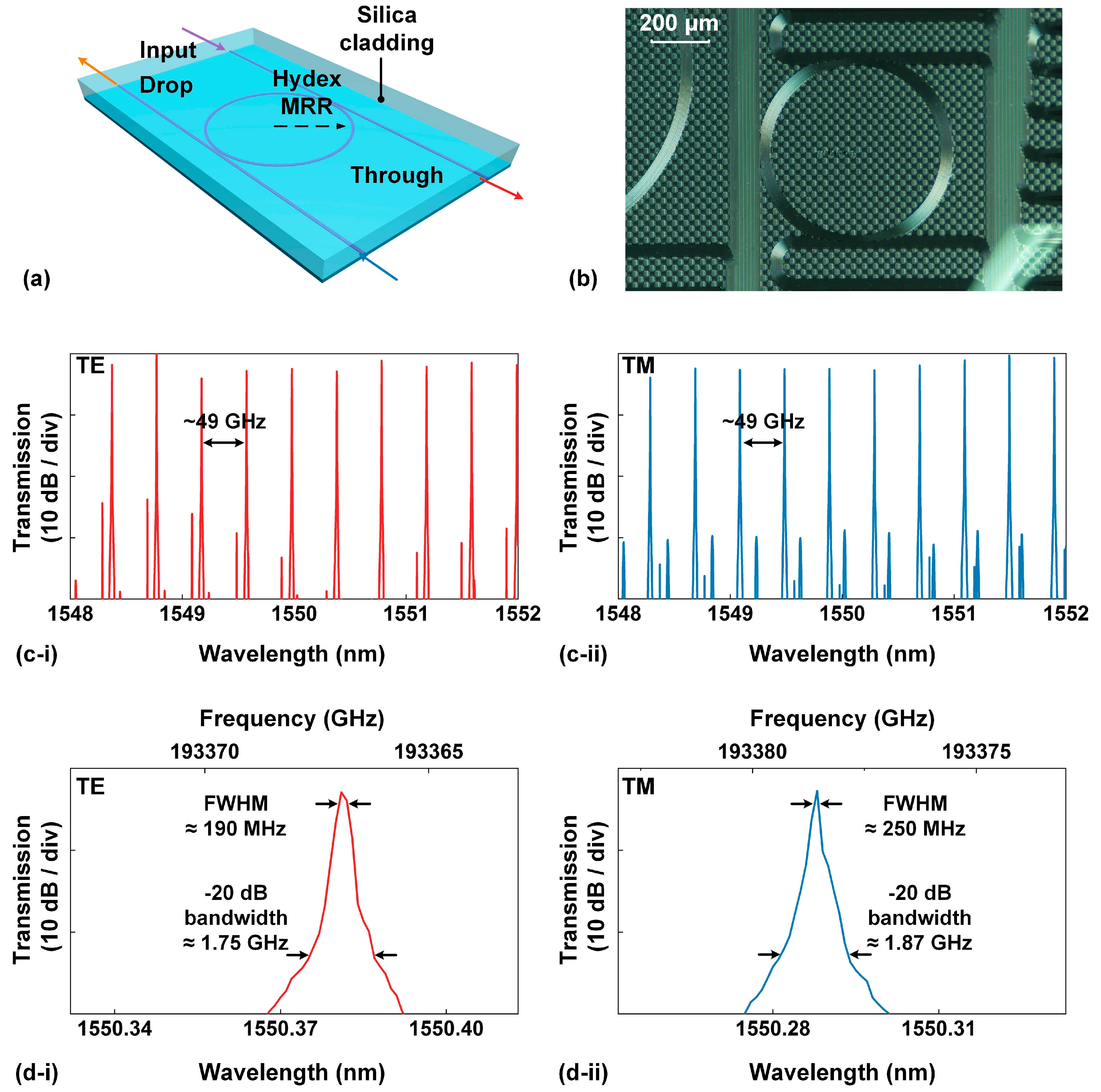
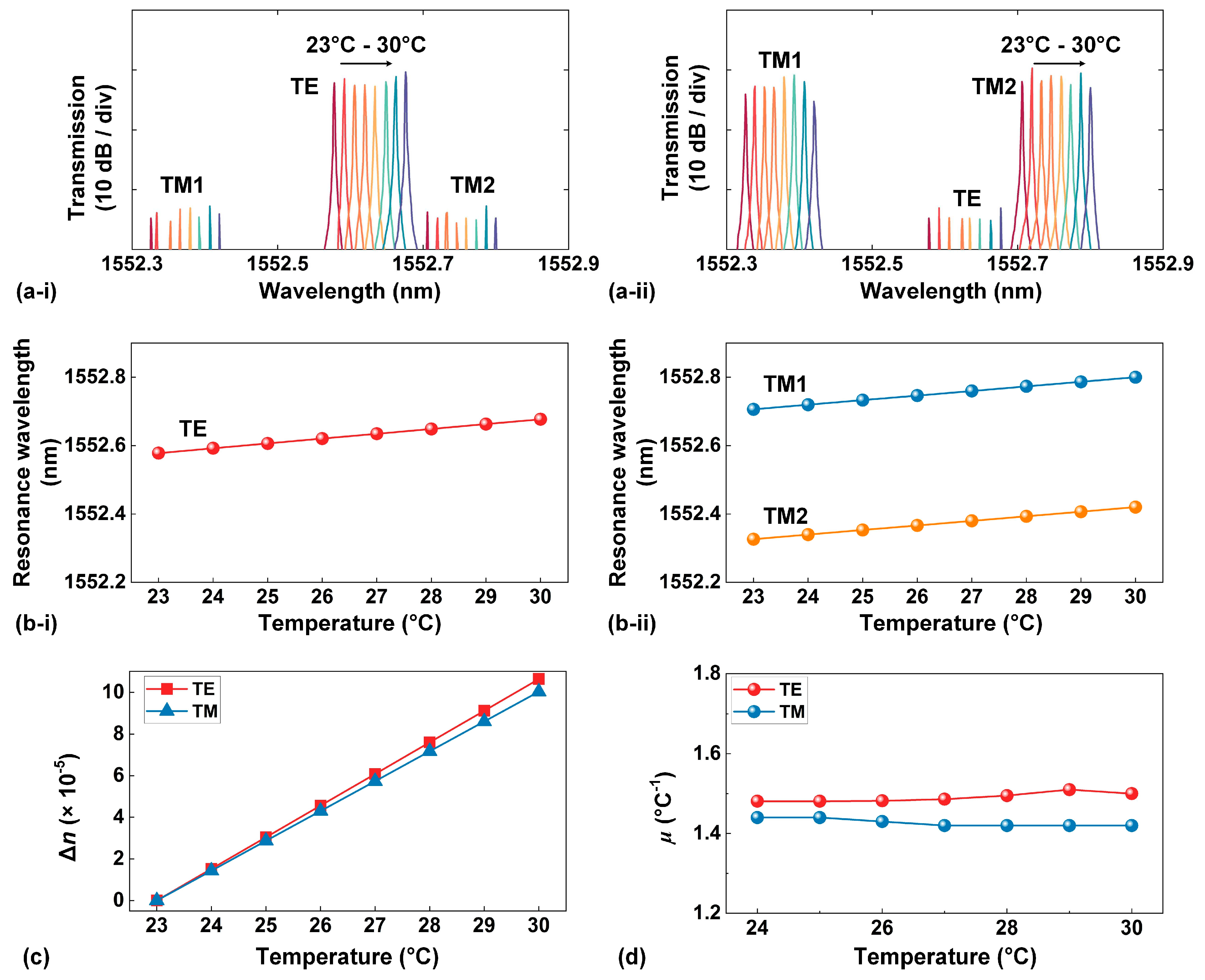
Disclaimer/Publisher’s Note: The statements, opinions and data contained in all publications are solely those of the individual author(s) and contributor(s) and not of MDPI and/or the editor(s). MDPI and/or the editor(s) disclaim responsibility for any injury to people or property resulting from any ideas, methods, instructions or products referred to in the content. |
© 2023 by the authors. Licensee MDPI, Basel, Switzerland. This article is an open access article distributed under the terms and conditions of the Creative Commons Attribution (CC BY) license (http://creativecommons.org/licenses/by/4.0/).


