Preprint
Article

Experimental Research on the Possibility of Recycling Silicon and Glass from Waste Photovoltaic Modules

This version is not peer-reviewed.

Submitted:

12 September 2023

Posted:

13 September 2023

You are already at the latest version

Abstract
The rapid development of the photovoltaic (PV) industry will result in an increase in the amount of electrical and electronic waste from used PV panels. Only in Poland, the total capacity installed in photovoltaic sources in Poland in May 2020 exceeded 1,950 MW, and the installation weight was approximately 120,000. tone. The problem arises in the recycling or management of this waste. This work presents methods used to recycle waste into photovoltaic modules. The authors investigated the possibility of mechanical and chemical processing of crystalline silicon. A method of thermal treatment of the panel was also proposed. As a result of the research, it was found that the stage of separating materials (crystalline cream, EVO foil, aluminum frame) plays an important role in the recycling process, which is not easy. Chemical treatment allows the silicon to become plastic and the temperature melts the back layer of the panel.
Keywords: 
Subject: 
Engineering  -   Energy and Fuel Technology

1. Introduction

There is currently a moderate amount of photovoltaic waste on the global market, so there is insufficient incentive to set up facilities dedicated to recycling photovoltaic (PV) panels. Once the panel is fully operational, it is typically processed at an existing general recycling facility. The scope of work includes a mechanical process of separating the main components of the materials that make up the panel. Material recovery depends on the weight of the panels. Some higher value materials (small amounts in the total weight of the panel) cannot always be completely recovered [1].
The current waste management strategy does not require recycling of devices from photovoltaic systems. Nevertheless, it is necessary to take into account the longer perspective and the need to consider building plants dedicated to the recycling of photovoltaic panels. This approach can increase the processing capacity of panels, maximize revenues and contribute to the protection of the natural environment, and most importantly, contribute to increasing the recovery of valuable components [2,3]. The classification of waste from the dismantling of photovoltaic panels is consistent with the basic classification of waste division. It takes into account the material composition of cells according to mass or volume and the properties of the components used in production and materials. The properties of materials include: solubility, flammability, and toxicity [1]. The overall goal of the recycling procedure is to identify the environmental hazards and human health impacts that may arise from storing the device at end-of-life. When indicating the need for recycling, the elements should be properly classified and then an appropriate disposal path should be selected to minimize the risks. A very important and important issue for the environment is the risk of leakage of materials from products not in use. Assessing this phenomenon improves and helps implement mitigation measures. Another example of waste characterization is determining the level of hazard - flammability and the impact of fumes and fumes from combustion. These factors, along with the degree of risk, depend on a given country and the judicial law in a given country [4]. The division of waste management from equipment after the end of its operation takes into account the following stages: waste generation, collection, transport, processing and disposal. In practice, this system is based on the collection, storage, treatment, recovery and recycling of waste. PV panels are stored at appropriately adapted points and then transported to a concentrated central location where further steps in this action can be taken [1]. In the first stage, the waste product is divided into individual materials (plastics, glass, metal, etc.). This is followed by the next step in the recovery process, taking into account the various material recycling streams. The degree of harmfulness of the materials, their usefulness and the possibility of further fractionation are taken into account. Each stage generates costs, which should be included, for example, in the original price of the device, in this case a PV panel [1,5]. Therefore, the financial system for processing elements must be based on the prior collection of information on the amount of recovered materials in recycling processes, the type of these materials, taking into account significant costs, among others. transport and, ultimately, revenues from the recycling process. The system defining the financing and management process determines the overall costs of the entire technology process, based on the waste processing process and the recycling process of photovoltaic panels [1,6]. In the case of PV recycling, recycling processes will mainly focus on recovering components such as glass, aluminum, copper and rare materials such as silver, indium and cadmium, which, when recovered even in small quantities, reduces the risk of its dangerous and toxic effect on the environment [4,5]. The biggest challenges in PV recycling are the separation or complete removal of (ethyl-vinyl acetate). For this purpose, various methods have been tested for the effectiveness of layer separation, such as mechanical crushing, thermal treatment, organic solvents, pyrolysis, vacuum sandblasting [6].
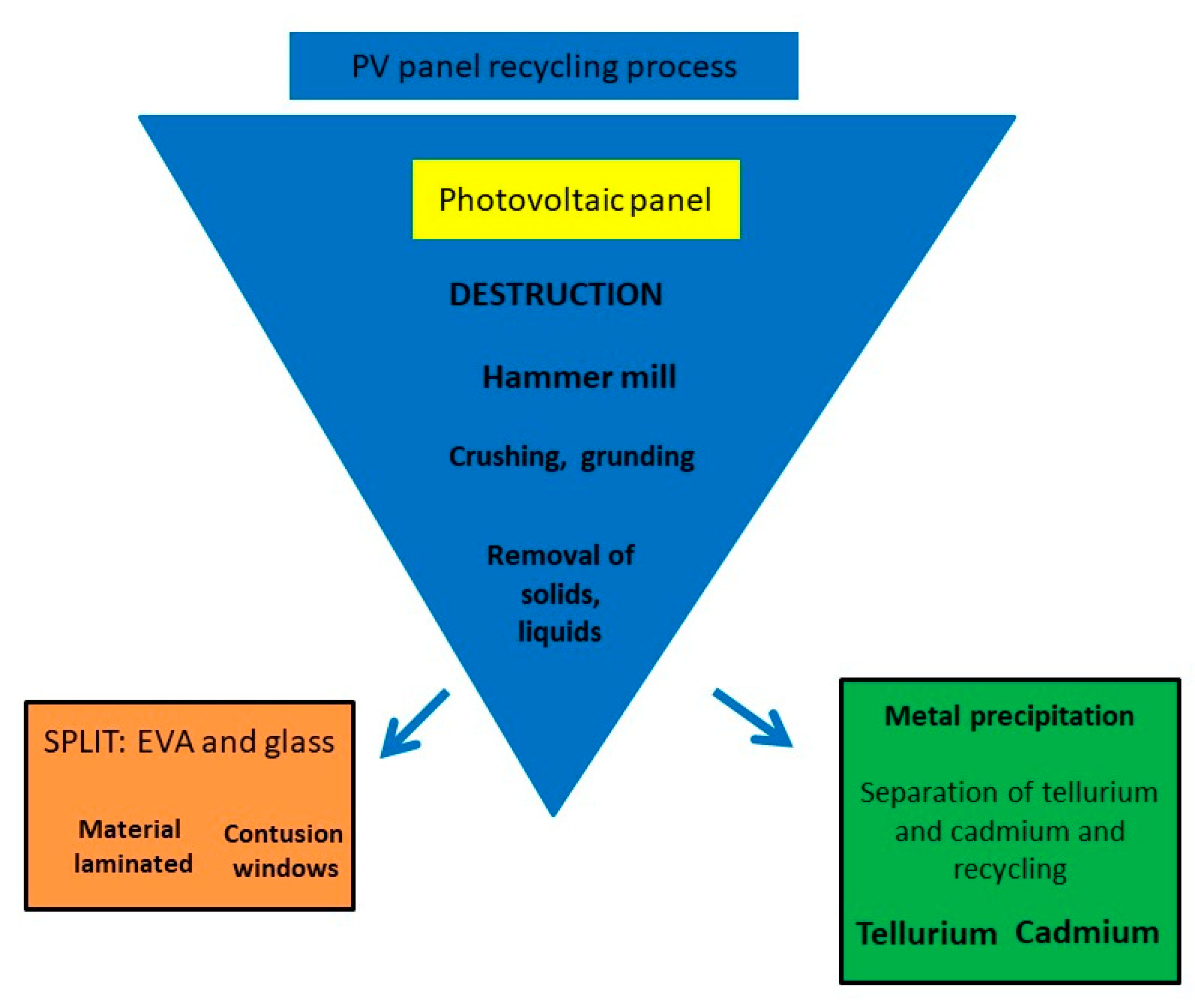
Figure 1 shows the methods used in the recycling stage. Recycling of photovoltaic panels is based on processing the material in such a way that it becomes a substance of primary importance. Recycling of materials based on the mechanical processing of waste uses shredding, grinding and mixing processes. The chemical method is based on the recovery of raw materials through ongoing processes and chemical reactions, such as digestion with alkalis, digestion with acids of various concentrations and at various times during the process. The chemical method produces silicon powder, which comes from silicon cells that are no longer suitable for further use. The scope of the chemical process includes alkali etching, which aims to remove the layer consisting of metal, in the case of panels it is aluminum, and acid etching to eliminate the p-n junction, rinsing [7,8]. The physical method is based on magnetic, electrostatic and eddy current separation, i.e. the separation of key components [9,10]. Using these methods, the waste is subjected to phase transfer separation using electrophoresis and gravity deposition [11].
The advantages and disadvantages of the processes currently used in the recycling process are presented in Table 1. During the analysis, the processes of breaking down the separation layers and removing the materials required for recycling were detailed. These technologies include filtration, centrifugation, phase transfer separations, electrophoresis, hydrobromination, sedimentation and leaching, electrokinetic separation, and hydrometallurgy. Each of these technologies is focused on the most cost-effective method and high material purity class.
The recycling scheme of photovoltaic panels is shown in Figure 2. In the first stage, the panels are shredded and crushed with a hammer and ground to break the laminated bond. Then the dust is collected in a system that is equipped with a high-efficiency particulate air filter. The next step is to etch the semiconductor layer with sulfuric acid and hydrogen peroxide. The glass is etched with ethyl vinyl acetate, and larger pieces that have not been digested are then separated in a classifier. Finally, the glass is thoroughly rinsed with water and the drying stage begins [1].
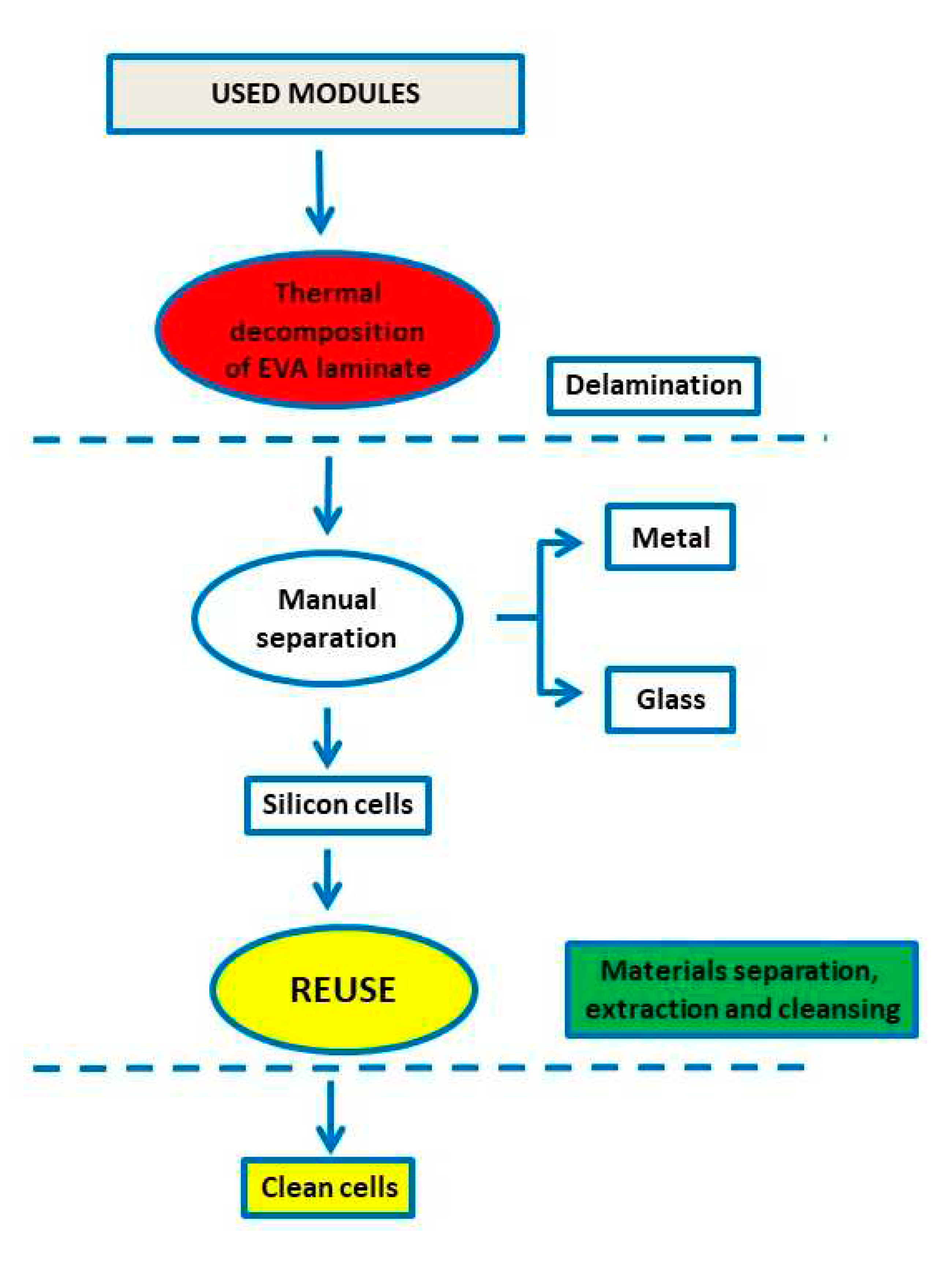
Every company that recycles photovoltaic panels relies on the same methods used to separate used material. Figure 3 shows how the German company SolarWord deals with recycling photovoltaic panels [14]. In the thermal process, plastic components are fired in a complex protective semiconductor at a temperature of 600 ° C, other materials such as solar cells, glass and metals are separated manually. Metal and glass are sent for recycling. Then the silicon wafers are etched again. The use of such a process recovers 84% of the mass of the output module, 90% of the glass is recovered for use in a new PV panel, 95% of semiconductor materials for use in cell production [10]. SolarWord's recycling methods are as follows:
• delamination,
• separation of materials,
• extraction and purification of material.
The delamination process is one of the most expensive processes in recycling. The laminate consists of EVA, and the back of the module is protected with a layer of Tedlar (a foil consisting of polyvinyl fluoride), which has many factors resistant to changing climatic conditions and mechanical properties. One of the delamination methods, which is considered one of the cheapest techniques, is the disintegration of grinding of entire photovoltaic modules or cutting off the laminate layer together with the glass plate. This method is impossible to achieve because adhesion occurs, i.e. strong adhesion of the sealing layer [16].
In the process of recycling used or damaged photovoltaic panels, the following processes are also used [16]:
• microemulsion method,
• crushing process of photovoltaic modules in liquid nitrogen, temperature -196 ° C,
• thermal decomposition,
• dissolving the foil in an organic solvent (e.g. acetone, gasoline, isopropanol, glycerin, tetrahydrofuran).
Some solvents used when dissolving EVA may cause its volume to increase, resulting in a crack in the plate cell. The solution to this problem is to distribute the force over the entire glass cover and flow out the excess EVA, leaving the silicon wafers intact. Most solvents also cause the material to swell [16].
The problem of managing materials from used photovoltaic panels already appears in many countries. The WEEE Directive (Waste of Electrical and Electronic Equipment) broadly presents waste management procedures and related regulations regarding electronic and electrical waste, the division of waste into selections, the technology process from processing, through recovery, to the disposal of harmful substances. threatening the natural environment [17,18]. Table 2 presents data on e-waste production and recycling by continent. The data below shows a graphical representation of how the amount of waste produced that requires compliance with appropriate procedures regarding its end of consumption is distributed. Asia dominates the production of electronic waste compared to all continents. Analyzing data on the amount of e-waste recycled expressed in %. Europe has a particularly significant advantage, with a high percentage of 42.5%.
In the context of the increasing amount of waste from photovoltaic installations, the authors of the study conducted research on the possibility of utilization and/or recycling of PV panels using the selected methods described above.
The work presents the results of experimental research using destroyed photovoltaic modules and an analysis of the possibilities of recycling polycrystalline silicon and glass as basic materials used in the construction of modules. Chemical methods using alkali and sulfuric acid (VI) of two concentrations were used. Regardless of the currently used methods, it has been proposed to use thermal treatment of cut PV panel elements together with microscopic analysis after processing.

2. Materials and Methods

2.1. Properties of the photovoltaic panel

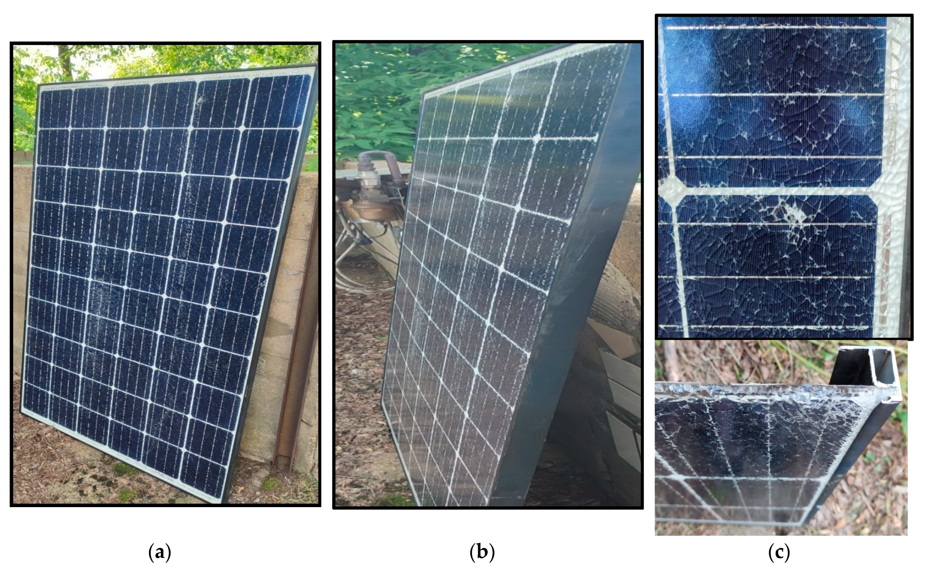
Photovoltaic panels damaged during transport were used for the tests. The figure (Figure 4. a, b) shows a monocrystalline (mono C - Si) photovoltaic panel with dimensions of 165 cm x 100 cm, suitable for recycling and subsequent processing into waste and recycling. There are visible cracks in the silicon crystal and glass on the module surface, which were caused by incorrect transport. This type of damage may also be caused by weather conditions. Strong winds, lightning storms and snow carry the risk of damaging photovoltaic panels. The scratches and cracks shown in Figure 4c cause the panels' resistance to strong impacts to decrease dramatically. Additionally, damage to the panel and disruption of its structure results in reduced efficiency and its operation. Microcracks increase the temperature and may burn through the foil that protects the module. Figure 4c shows a view of the crack and the microcracks around it contributing to a serious failure in the entire system.
The entire module is enclosed in an aluminum frame surrounding the entire panel. Figure 4 c shows the thickness of the frame located around the entire photovoltaic module. Such a damaged module, just like modules worn out as a result of long-term operation, should also be dismantled in an appropriate manner and then recycled or stored in appropriate conditions. In order for the entire photovoltaic module to function properly and avoid failure, everything must fit tightly together. As you can see in the cross-section, the panel consists of several layers closely adhering to each other. Aluminum elements play a large part in the recycling process of photovoltaic modules. Figure 4b and 4d show a side view of the module and a top view, showing the aluminum frame in which the photovoltaic panel is located.
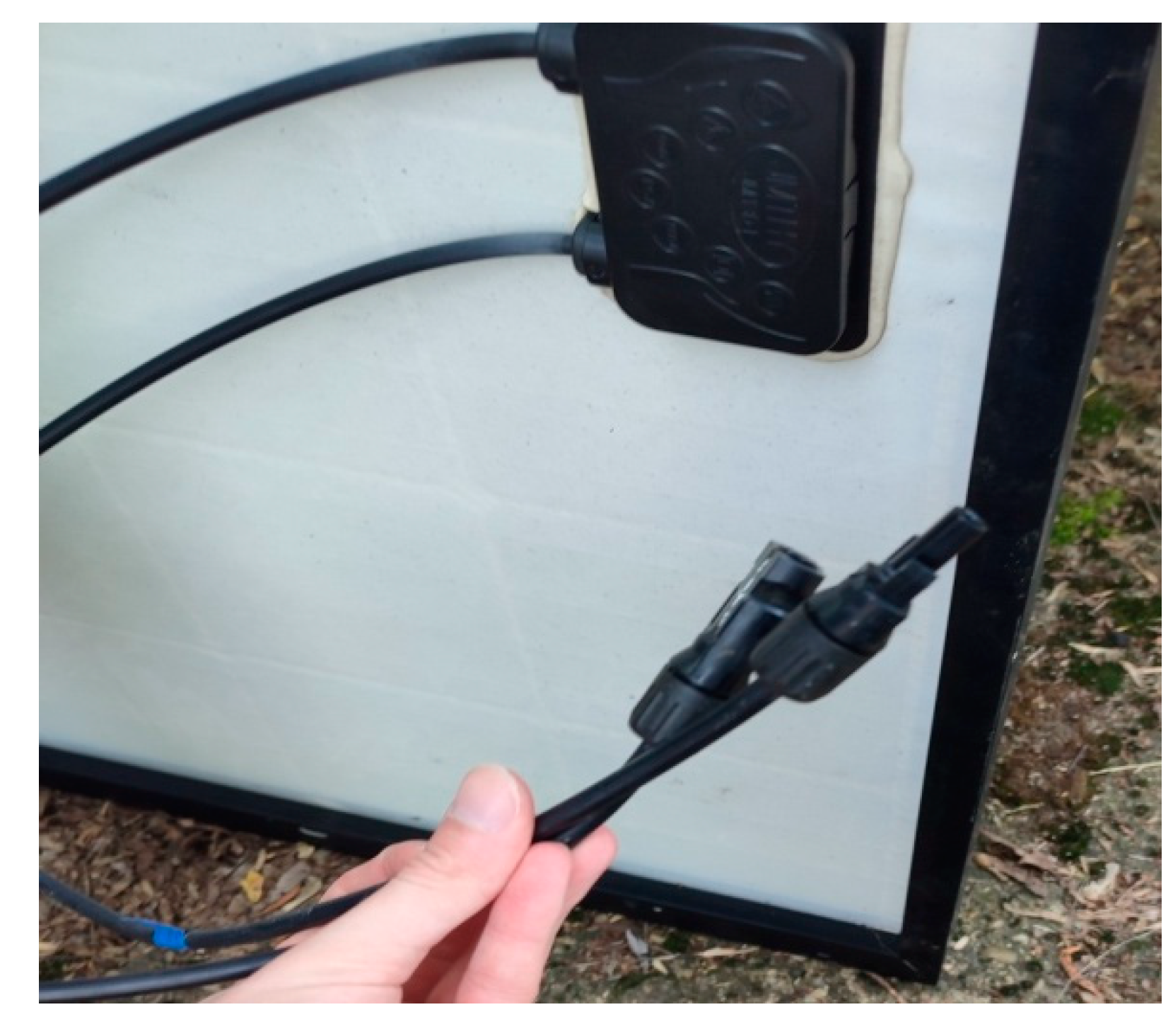
An important element of the panel in terms of its operation and disposal as a large electronic device is the junction box that allows for safe cable routing. Figure 5 shows the rear part of the module. The figure shows MC4 connectors used to connect wires in the junction box or individual cells. MC4 connectors are the best solution to ensure the safety of PV installations and proper contact between individual modules.

2.2. Dismantling a monocrystalline photovoltaic panel

Figure 6 shows samples that were cut out from the photovoltaic module discussed in the above chapter. Due to the very difficult disassembly of the panel, the samples were cut using an electric saw. Cutting the module and separating the individual layers is extremely difficult and requires specialized tools.

2.3. Methods used when analyzing the recyclability of materials used to build a photovoltaic module

The analysis of the materials from which the photovoltaic modules were made was carried out using a MicroCapture microcamera equipped with a program enabling photo analysis. Thanks to the function of angle analysis, grain size analysis, and thickness of individual layers, changes caused by mechanical damage to the module and changes after exposure of the module in solutions were determined.

2.4. Chemical methods

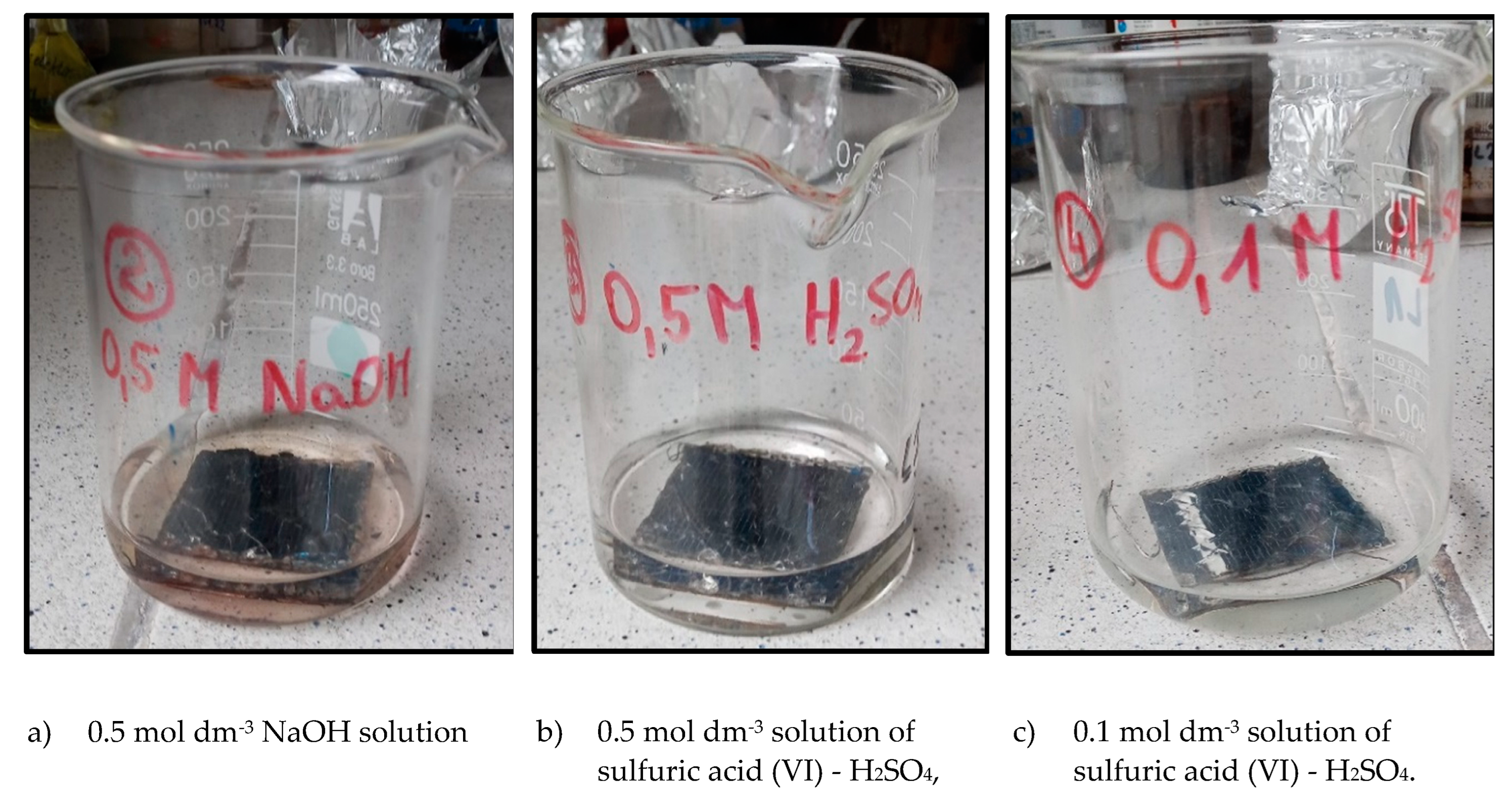
One of the methods to separate individual elements of a photovoltaic module is to expose the elements to acidic or alkaline solutions. As part of this work, the following solutions were used, in which samples were exposed for 34 days in each of the analyzed solutions (Figure 7):
• 0.5 mol dm-3 NaOH solution,
• 0.5 mol dm-3 solution of sulfuric acid (VI) - H2SO4,
• 0.1 mol dm-3 solution of sulfuric acid (VI) - H2SO4.

2.5. Thermal method

The method enabling the decomposition of individual elements of a photovoltaic module proposed by the authors is the thermal method. Photovoltaic panel samples were exposed to high temperatures ranging from 200 to 500oC. The PV panel samples were heated without air. Each sample was placed in a tight can and placed in an oven heated to the appropriate temperature. The sample stayed in the oven for 15 minutes, then was removed and left to cool.

3. Results and discussion

3.1. Analysis of the change in mass of PV module samples

Table 3 and Table 4 present individual masses under specific conditions during laboratory tests.
The change in these masses was influenced by the acid in which the sample was placed. The action of sulfuric acid (VI) caused significant changes in the mass values and caused the EVA film polymer to swell. Sulfuric acid, but also sodium hydroxide, which caused changes in the external structure, i.e. the glass on the panel surface, through numerous pits and changes under the glass surface. After drying the samples subjected to previous chemical processes, the mass value decreased due to the evaporation of the liquid.

3.2. Structural analysis of PV module samples after exposure in solutions

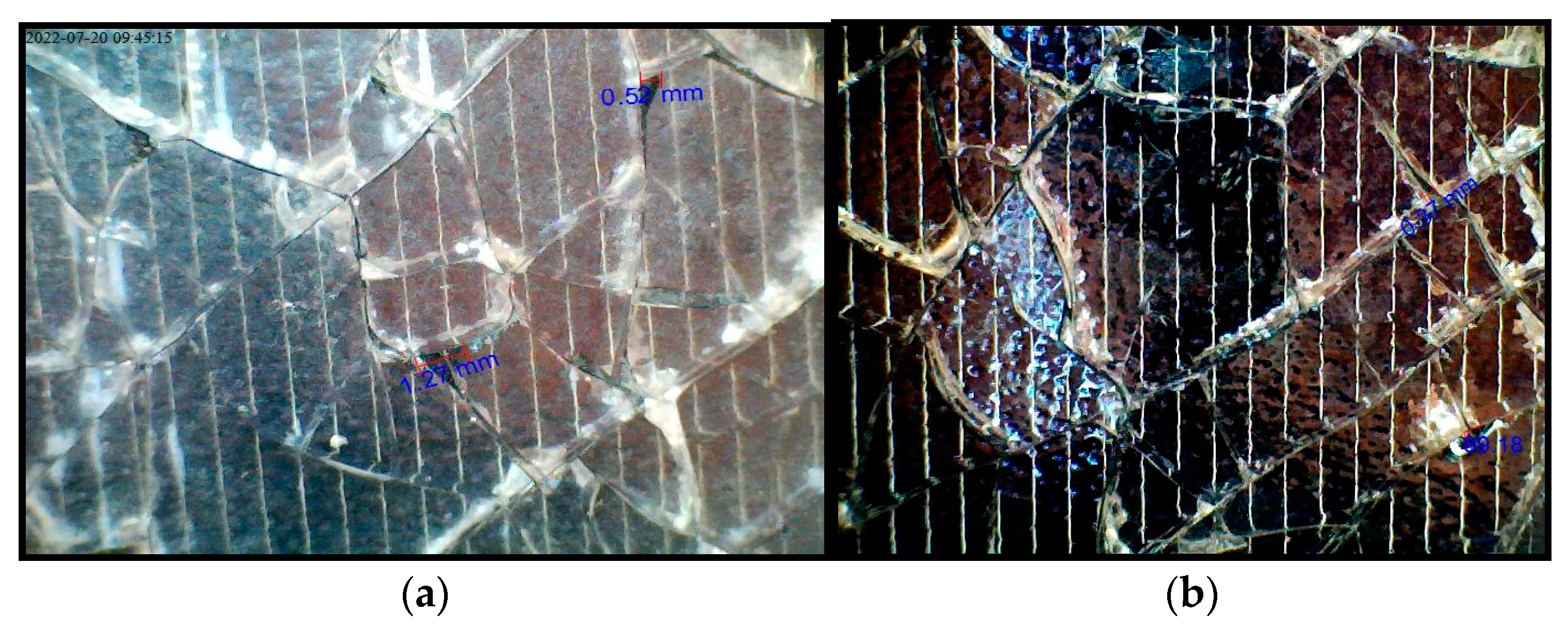
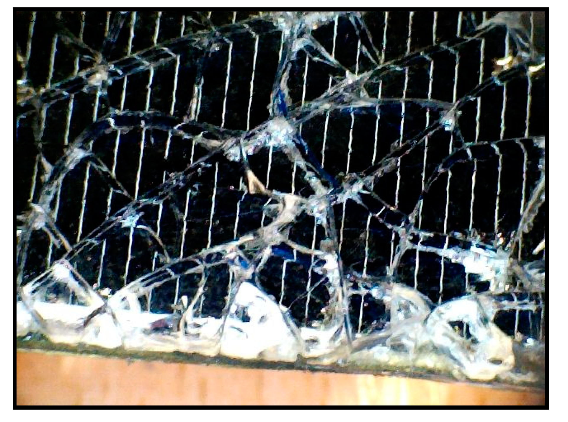
Below are the samples after thorough drying after exposure for 34 days in each of the analyzed solutions. Figure 8 shows a view of a sample immersed in a 0.5 mol dm-3 NaOH solution. A change in the color of the glass is visible on the surface due to the alkali penetrating under the surface, which also caused the appearance of pits. For example, one of the ones observed in Figure 8 has a size of 1.27 mm, while the other one is slightly smaller and is 0.52 mm.
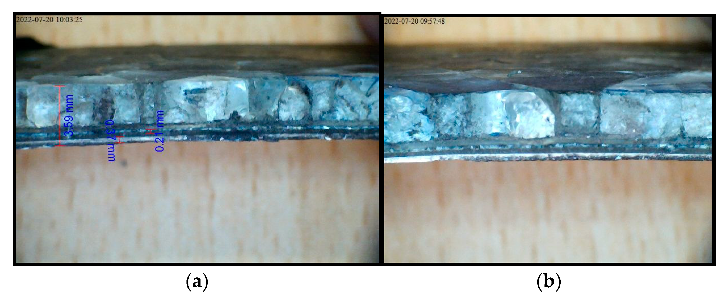
The material thickness of the photovoltaic module sample is shown in Figure 9. The total thickness of the module is 3.59 mm, distinguished by pure silicon - 0.37 mm, EVA foil - 0.21 mm and glass glass. According to the manufacturers' data, the thickness is 3.2 mm and is thermally reinforced.
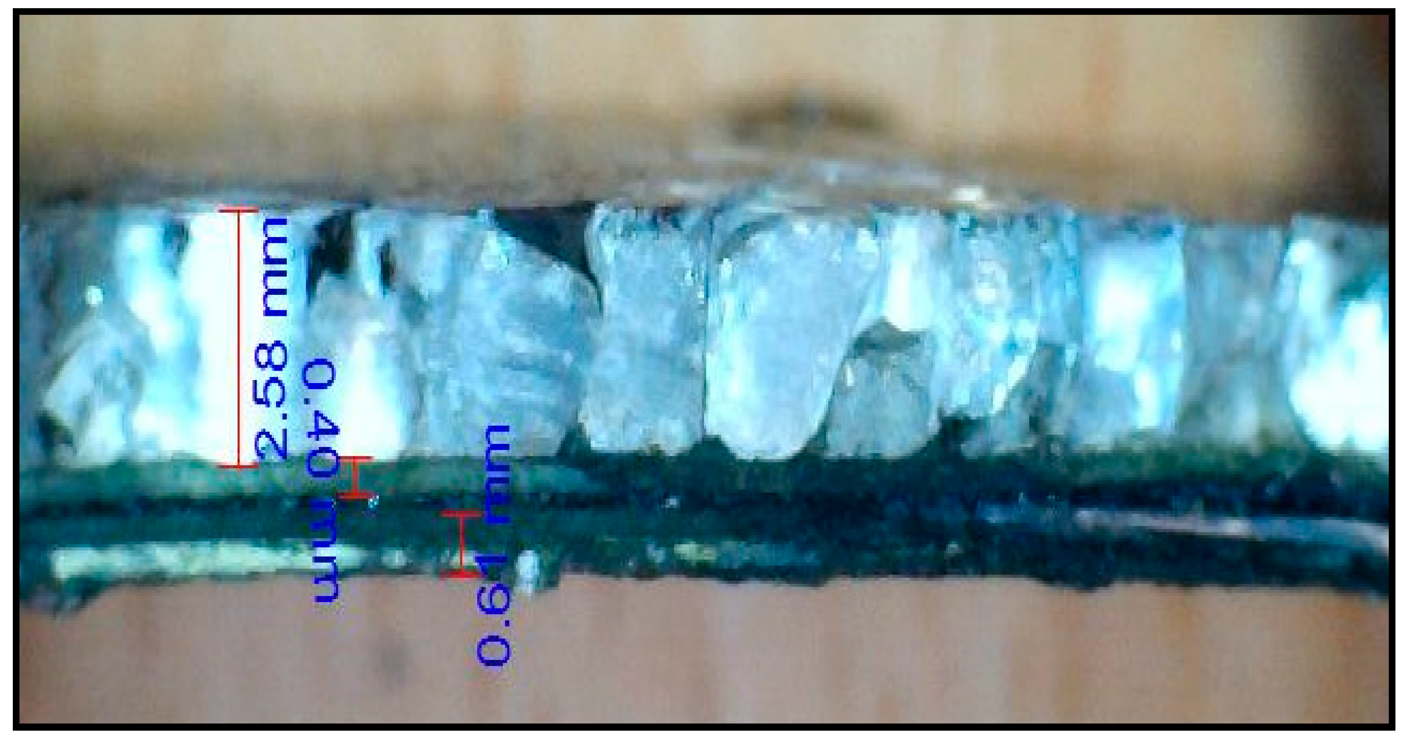
Figure 10 presents the thickness of individual layers of the sample after exposure to 0.5 mol dm-3 H2SO4 acid. The thickness of the glass protecting against mechanical damage is approximately 2.58 mm, the thickness of the EVA foil is estimated at approximately 0.40 mm, and the thickness of the crystalline silicon layer is approximately 0.61 mm.
After exposure of the sample, the so-called phenomenon was observed. swelling of layers, but it did not always occur in one place. Similar observations are reported by the author of work [16]. This is probably related to the penetration of the acid solution through the cracks of the panel submitted for testing, which was mechanically damaged during transport, therefore it was possible to carry out tests related to the attempt to dismantle the panel (Figure 11).

3.3. Analysis of thermal treatment of PV module Samales

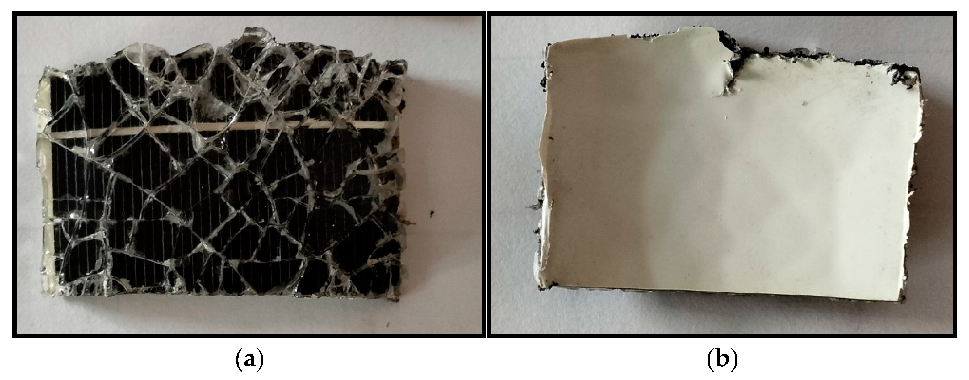
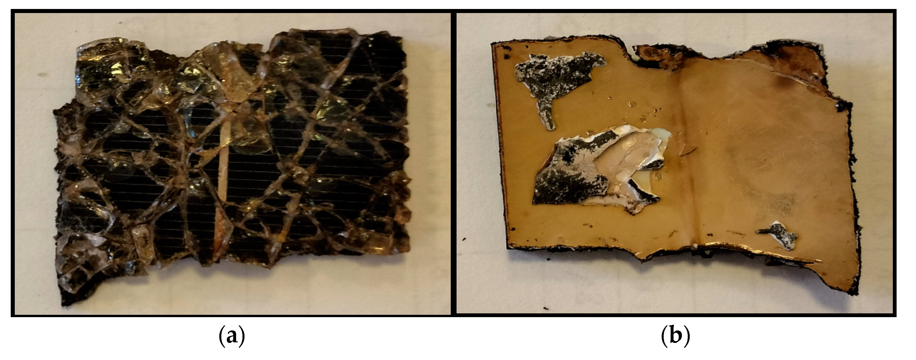
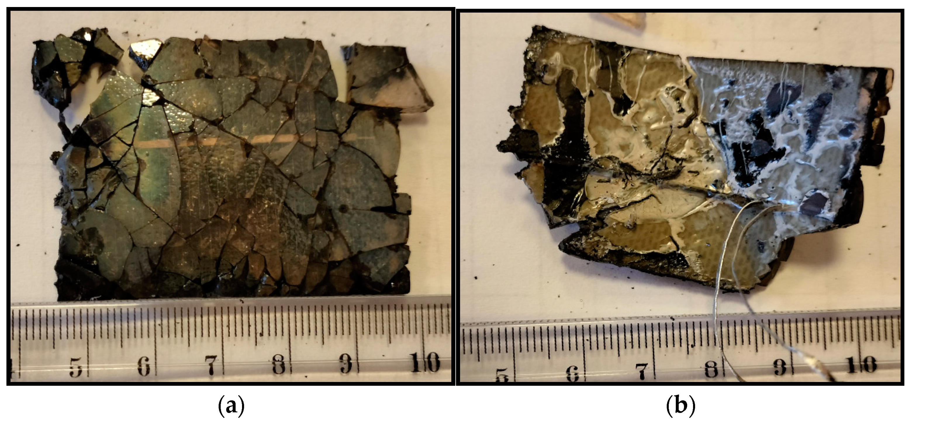
As written in section 2.5, the PV module samples were thermally treated at temperatures of 200, 300, 400 and 500oC.
A sample of the PV module heated at a temperature of 200oC is shown in Figure 12. At this temperature, the panel did not undergo any significant changes, and there was no change in the structure of the panel and in the ability to separate the glass layer from the rest of the panel.
Another sample of the PV module was subjected to a temperature of 300oC, as shown in Figure 13. At this temperature, the panel also did not undergo significant changes. The glass on the panel surface was slightly browned, just like the bottom of the panel, and there was no change in the structure of the panel or in the ability to separate the glass layer from the rest of the panel.
The next sample of the PV module was subjected to a temperature of 400oC, as shown in Figure 14. At this temperature, the panel underwent significant changes. The glass on the panel surface was heavily smoked, while the bottom layer of the panel was partially melted. As we can see in Figure 14a, the glass could be easily separated from the bottom layer of the panel (Figure 14b), and the bus bars could be easily separated from the glass.
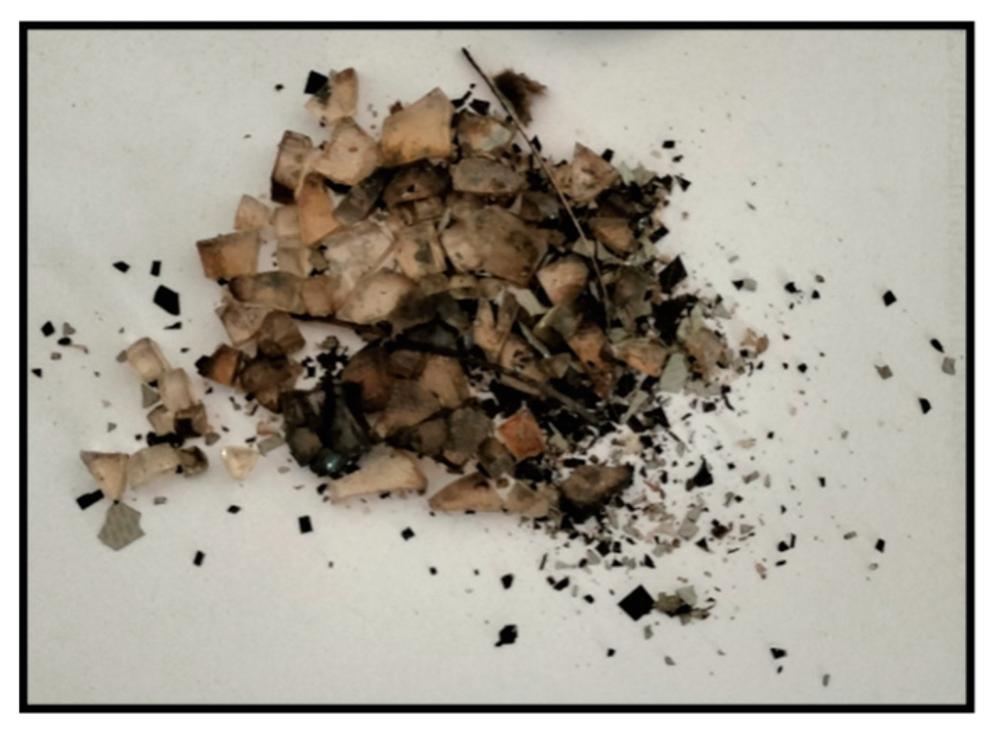
The last panel sample was exposed to a temperature of 500oC (Figure 15). After subjecting the panel to this temperature, the bottom layer of the panel was melted, leaving the glass in the form of shards that resulted from previous damage to the panel. Bus bars were intact and easily accessible.

4. Conclusions

As part of the work, research was carried out to identify simple methods for dismantling a photovoltaic panel, up to recycling individual metals and reusing them in industry. Based on the literature and laboratory research carried out, the following conclusions were formulated:
  • the number of used photovoltaic modules is increasing in Poland and around the world, which generates problems with electronic waste management,
  • proper waste management and storage depends on the degree of raw material recovery and the type of recovered materials,
  • the conducted research has proven that the disassembly of the photovoltaic module, i.e. the separation of individual layers (glass - EVA foil - crystalline silicon) is very difficult and requires special tools, at the same time the use of mechanical methods, i.e. mills, grinding, grinding, separation, is associated with a large energy consumption;
  • as a result of exposure of module elements in acidic solutions, the solution penetrated the material and caused changes in the sample in the form of cracks and plasticization of the sample;
  • after exposure of the module samples for 34 days, an increase in mass was observed both in the solution of 0.5 mol dm-3 NaOH, as well as in 0.1 mol dm-3 and 0.5 mol dm-3 H2SO4, which may result from the phenomenon liquid absorption through EVA foil. After drying the samples, a weight loss of 0.0585 g was observed in an alkaline solution (0.5 mol dm-3 NaOH) and from 0.0016 g and 0068 g in solutions of 0.1 mol dm-3 and 0.5, respectively. mol dm-3 H2SO4;
  • the phenomenon of swelling of material samples was supported by the analysis of the thickness of the samples: after exposure, the total thickness of the module was estimated at approx. 3.59 mm (crystalline silicon: approx. 0.37 mm, EVA foil: approx. 0.21 mm, tempered glass: and glass pane: approx. 3.00 mm), according to the manufacturer, the panel thickness is 3.2 mm;
  • after thermal treatment of the panel at a temperature of 500oC, the bottom layer of the panel was melted, the glass was in the form of crumbs, which resulted from previous damage to the panel. Bus bars were intact and easily accessible.

Author Contributions

For research articles with several authors, a short paragraph specifying their individual contributions must be provided. The following statements should be used “Conceptualization, R.W. and M.W.; methodology, R.W.; software, K.K.; validation, R.W., M.W.; formal analysis, R.W.; investigation, M.W. K.K..; resources, K.K.; data curation, R.W., M.W.; writing—original draft preparation, K.K., R.W..; writing—review and editing, R.W.; visualization, R.W., K.K.; supervision, M.W. All authors have read and agreed to the published version of the manuscript.” Please turn to the CRediT taxonomy for the term explanation. Authorship must be limited to those who have contributed substantially to the work reported.

Funding

The scientific research was funded by the statute subvention of Czestochowa University of Technology, Faculty of Infrastructure and Environment. The research was funded by the project No. BS/PB400/301/23.

References

  1. www.flixenergy.pl/-recyklingu-modulow-pv-zagrozenie-w-przyszlosci-czy-potencjalny-biznes,dn.05.03.2022.
  2. End-of- live management Solar Photovoltaic Panels, IRENA International Renewable Energy Agency (access August 2023).
  3. www.evertiq.pl/news/28867,dn.06.03.2022.
  4. Stowarzyszenie Technologii Ekologicznych Silesia, Sprawdzone metody gospodarowania odpadami komunalnymi, in polish (access August 2023).
  5. Postępowanie z odpadami komunalnymi po przetworzeniu w instalacjach mechaniczno-biologicznego przetwarzania odpadów komunalnych (MBP), Departament Środowiska, Najwyższa Izba Kontroli, in polish (access August 2023).
  6. www.energetyka24.com/recykling-w-fotowoltaice-czy-poradzimy-sobie-ze-starymi-panelami-analiza, in polish (access August 2023).
  7. Adam Mroziński, Wydział Inżynierii Mechanicznej, Uniwersytet Technologiczno Przyrodniczy, Bydgoszcz, Nr 5/2010,Recykling ogniw fotowoltaicznych,dn.30.03.2022.
  8. Ewa Radziemska, Piotr Ostrowski, Tomasz Seramak, Obróbka chemiczna krzemowych ogniw słonecznych jako najważniejszy etap w recyklingu modułów fotowoltaicznych,dn.30.03.2022.
  9. Technologia monokryształów i cienki warstw, (access August 2023).
  10. www.sites.google.com/site/profesorjanczochralski/in-the-news, (access August 2023).
  11. www.centrumnaukiec1.pl/aktualnosci/monokrysztaly-jana-czochralskiego, (access August 2023).
  12. Jing Tao, Suiran Yu, ELSEVIER, Review on feasible recycling pathways and technologies of solar photovoltaic module, (access August 2023).
  13. End-of- live management Solar Photovoltaic Panels, IRENA International Renewable Energy Agency (access August 2023).
  14. Jing Tao, Suiran Yu, ELSEVIER, Review on feasible recycling pathways and technologies of solar photovoltaic module, (access August 2023).
  15. SolarWorld AG | www.pvinfo.pl (access August 2023).
  16. Anna Kuczyńska- Łażewska, Technologie recyklingu zużytych odpadowych modułów fotowoltaicznych I i II generacji, (access August 2023).
  17. Dyrektywa Parlamentu Europejskiego I Rady 2012/19/UE z dnia 4 lipca 2012 r. w sprawie zużytego sprzętu elektrycznego i elektronicznego (WEEE).
  18. Raport o funkcjonowaniu systemu gospodarki zużytym sprzętem elektrycznym i elektronicznym w 2017 roku, (access August 2023).
  19. Europejski Trybunał Obrachunkowy, Działania UE dotyczące odpadów elektronicznych i wyzwania w tej dziedzinie 2021, (access August 2023).
  20. Raport Gospodarka elektrodpadami. Wyzwania na lata 2019-2023. Analiza sytuacji na rynku gospodarowania zużytym sprzętem elektrycznym i elektronicznym oraz rekomendacje, (access August 2023).
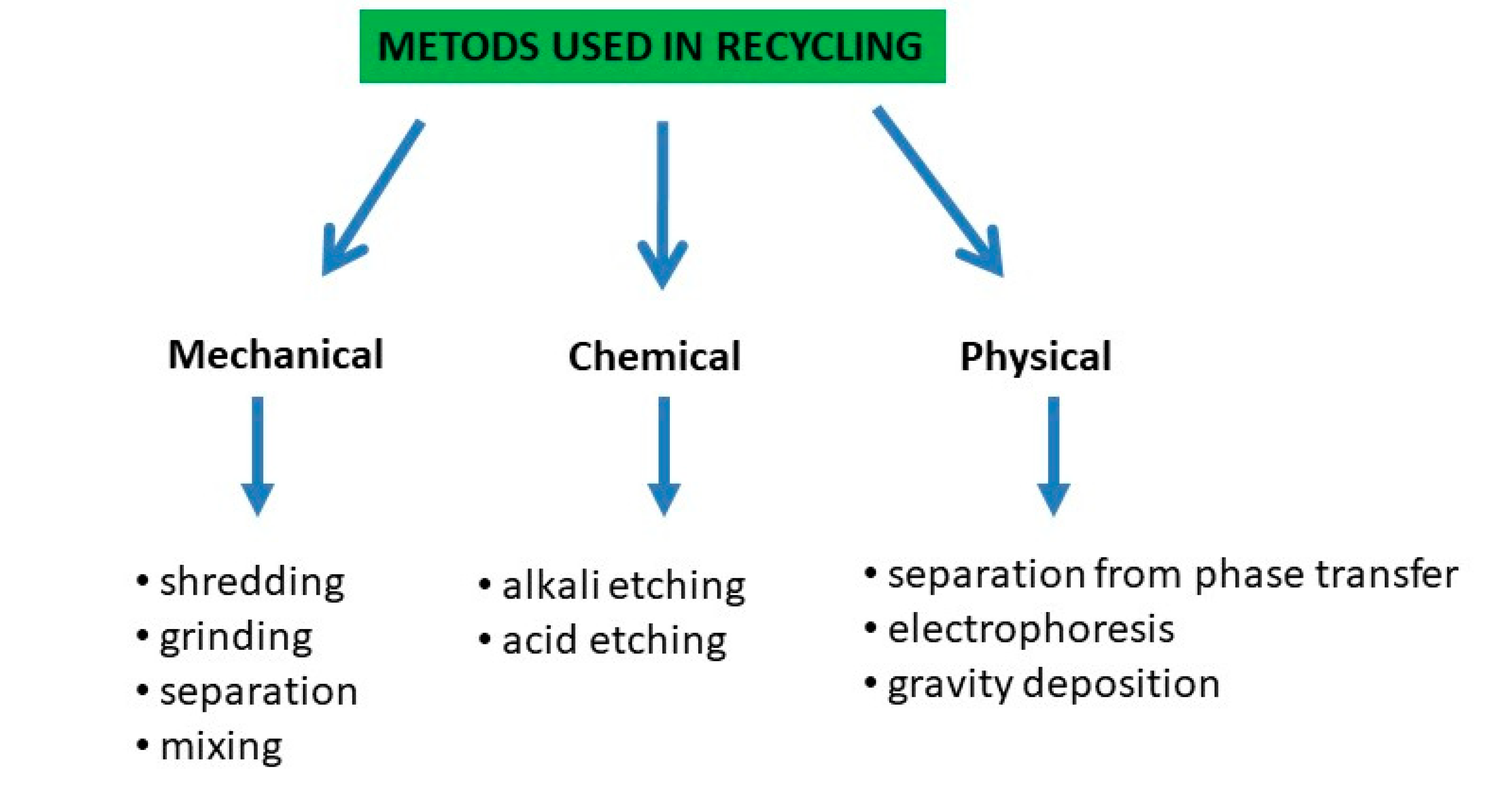
Figure 1. General division of methods used to separate used materials.
Preprints 84906 g001
Figure 2. PV panel recycling process [13].
Preprints 84906 g002
Figure 3. The recycling process of the German company SolarWord [15].
Preprints 84906 g003
Figure 4. Photovoltaic module with visible cracks due to incorrect transport.
Preprints 84906 g004
Figure 5. The rear part of the module with a visible junction box and cable outlets using MC4 connectors.
Preprints 84906 g005
Figure 6. Samples cut from a monocrystalline photovoltaic module.
Preprints 84906 g006
Figure 7. Exposure of photovoltaic module samples in solutions.
Preprints 84906 g007
Figure 8. Observing the pitting occurring during testing on a photovoltaic panel sample.
Preprints 84906 g008
Figure 9. a) total thickness of individual components of the photovoltaic panel expressed in dimensions, b) internal cross-section of the layers of the photovoltaic panel.
Preprints 84906 g009
Figure 10. Including measurements of specific layers of the sample after exposure to 0.5 mol dm-3 H2SO4 acid.
Preprints 84906 g010
Figure 11. Presentation of the effect of acid on the structure of the sample, causing numerous changes on the surface of the glass and under the inner layer.
Preprints 84906 g011
Figure 12. PV panel exposed to a temperature of 200oC for 15 minutes, view a) from above and b) from below.
Preprints 84906 g012
Figure 13. PV panel exposed to a temperature of 300oC for 15 minutes, view a) from above and b) from below.
Preprints 84906 g013
Figure 14. PV panel exposed to a temperature of 400oC for 15 minutes, view a) from above and b) from below.
Preprints 84906 g014
Figure 15. PV panel exposed to a temperature of 500oC for 15 minutes.
Preprints 84906 g015
Table 1. List of Technologies for recycling waste from PV module [12].
Technology PV module type Advantages and disadvantages
Filtration Crystalline silicon capable of filtering small-sized particles
contamination must be reduced before filtration
Spinning Crystalline silicon high silicon recovery content
time-consuming process
submicron SiC particles cannot be removed
Separation with phase transfer Crystalline silicon very high silicon recovery and
no use of aggravating liquid
very economical
Electrophoresis and gravity deposition Crystalline silicon very effective in the separation of Si, Al2O3
aluminum impurities in silicon
Electric field Crystalline silicon effective in the separation of silicon and SiC
no use of toxic substances
Pre-treatment is needed to eliminate contaminants from the metal
Al–Si alloying Crystalline silicon elimination of SiC
meticulous process
Hydrobromination Crystalline silicon recovery of high-purity silicon without SiC removal
Supercritical water Crystalline silicon obtaining silicon from oily waste after silicon ingot processes
Sedimentation and leaching Crystalline silicon separation of silicon and SiC using physical methods
a much easier process and not too complicated
Mono crystal Czochralski process Crystalline silicon mono crystal recovery
reducing boron, which facilitates efficiency
Electrokinetic separation Crystalline silicon high efficiency of removing iron fragments from waste
no chemical additives are used
Hydrometallurgy (oxidation, evaporation, reduction by inorganic substances) CIGS obtaining high-purity selenium
Hydrometallurgy
(dissolution, filtering, electroplating, extraction)
CIS application of typical hydro-metallurgical processes and use of chemicals
recovery of pure indium
further development of technology
Table 2. Number of e-waste production and number of e-waste recycled [19,20].
Continent Number of e-waste production [million tons] Number of e-waste production per capita [kg] Number of e-waste recycled [million tons] Number of e-waste recycled [%]
Africa 2.9 2.5 0.03 0.9
America 13.1 13.3 1.2 9.4
Asia 24.9 5.6 2.9 11.7
Europe 12 16.2 5.1 42.5
Oceania 0.7 16.1 0.06 8.8
Table 3. Showing detailed changes in the masses of the solution and the solution with the panel sample.
0.5 mol dm-3 NaOH 0.5 mol dm-3 H2SO4 0.1 mol dm-3 H2SO4
m0 14.7422 g 16.7304 g 16.5919 g
mzal 142.6702 g 152.2068 g 187.4988 g
m3 138.0130 g 148.6846 g 183.4708 g
m4 14.9688 g 16.9590 g 16.8485 g
m5 14.6837 g 16.736 g 16.5851 g
m6 122.9970 g 131.7030 g 166.5834 g
m0- mass of the cut PV module sample; mzal - mass of sample with solution; m3 – solution with the plate after 14 days; m4 – sample after removal – immediately; m5 – after drying for 24 hours in a dryer; m6 – solution without sample after 14 days.
Table 4. Presented mass values before and after drying the sample as part of laboratory tests.
0.5 mol dm-3 NaOH 0.5 mol dm-3 H2SO4 0.1 mol dm-3 H2SO4
mn 46.0325 g 51.0224 g 44.4226 g
mn+p 60.8585g 67.9300 g 61.1760 g
m after drying 60.7162 g 67.7544 g 61.0077 g
mn – mass of the pan; mn+p – mass before drying, pan+sample; m after drying – mass after drying; drying temperature - 40°C drying time - 24 h.
Disclaimer/Publisher’s Note: The statements, opinions and data contained in all publications are solely those of the individual author(s) and contributor(s) and not of MDPI and/or the editor(s). MDPI and/or the editor(s) disclaim responsibility for any injury to people or property resulting from any ideas, methods, instructions or products referred to in the content.
Copyright: This open access article is published under a Creative Commons CC BY 4.0 license, which permit the free download, distribution, and reuse, provided that the author and preprint are cited in any reuse.
Alerts
Prerpints.org logo

Preprints.org is a free preprint server supported by MDPI in Basel, Switzerland.

Subscribe

© 2025 MDPI (Basel, Switzerland) unless otherwise stated