1. Introduction
The utilization of tunable devices for high-frequency signal processing has been re-considered in the past years to provide the reconfiguration of systems to be used for satellite communications, where multi-band systems begin to be widely adopted. The choice of RF MEMS to overcome the intrinsic limitations of pin diodes or transistors using an all-passive solution has been debated for the last two decades. Despite the obvious advantages of using microelectromechanical systems, a fully reliable and long-lifetime solution has not yet been certified for the Space environment. On the other hand, a few examples of very reliable configurations for redundancy purposes [
1,
2] or for matrix configurations [
3,
4,
5] to be used in signal routing have also been studied in the past years. Research activities are still performed for Space applications [
6,
7]. For this reason, the RF MEMS solution is still appealing to substitute semiconductor conventional switches or even bulky waveguide switches with planar, miniaturized, and fully passive devices.
In this paper, RF MEMS devices will be used in a single-pole-double-through (SPDT) configuration to address the microwave signal in two branches loaded by resonators working at frequencies very close to each other (fine-tuning around 20 GHz or 26 GHz) or to switch the signal between 20 GHz and 26 GHz approx.
The general structure of the proposed devices has been designed in coplanar waveguide (CPW) configuration for possible implementation within staked modules, i.e., in situations where the electromagnetic interference between different layers must be minimized. The CPWs naturally fulfill this requirement because the electric field is confined in the plane of the substrate. In this framework, the clamped metal beams are the best mechanical structure to be used for RF MEMS switches. Manufacturing the micromechanical devices using the lateral ground planes for supporting the entire structure is convenient from a mechanical and electrical standpoint because it is easier to separate the RF and DC paths, as generally required by the high-frequency sub-systems.
Two geometries have been considered in this contribution: (i) triangular resonators with Sierpinski geometry and (ii) U-shaped resonators.
The Sierpinski structures have been introduced for a few reasons. First, triangular geometries are rarely used but have some advantages in terms of footprint and coupling possibilities, as discussed in [
8], with respect to square or circular resonators. Secondly, there is no systematic work or a straightforward analytical approach to determine the spectrum of the Sierpinski triangles depending on the internal complexity, and an experimental approach supporting or modifying the theory is necessary for CPW-fed configurations.
This paper has also studied the U-shape, combining two resonators with SPDT RF MEMS devices. In this case, we selected this configuration for miniaturization purposes and the possible utilization in coupled structures analogously to the classical hairpin filters developed in microstrip configuration [
9].
So far, the novelty of this basic work is mainly related to introducing the design of triangular and U-shaped resonators in a non-conventional configuration hosted by a CPW environment and driven by RF MEMS switches.
Results about the design, manufacturing, and testing of devices mounting RF MEMS SPDT switches will be presented for applications in K-Band, specifically working around 20 GHz and 26 GHz. The technology for realizing switches in MEMS technology has already been discussed in [
8] and will be briefly reviewed here. In this contribution, we shall discuss the advantages and drawbacks of the dual frequency and fine-tuning operations using switched resonators implemented by the RF MEMS technology. The electromagnetic high-frequency simulations are performed by the Cadence AWR Microwave Office package V22.1, using the Axiem® solver.
2. SPDT design
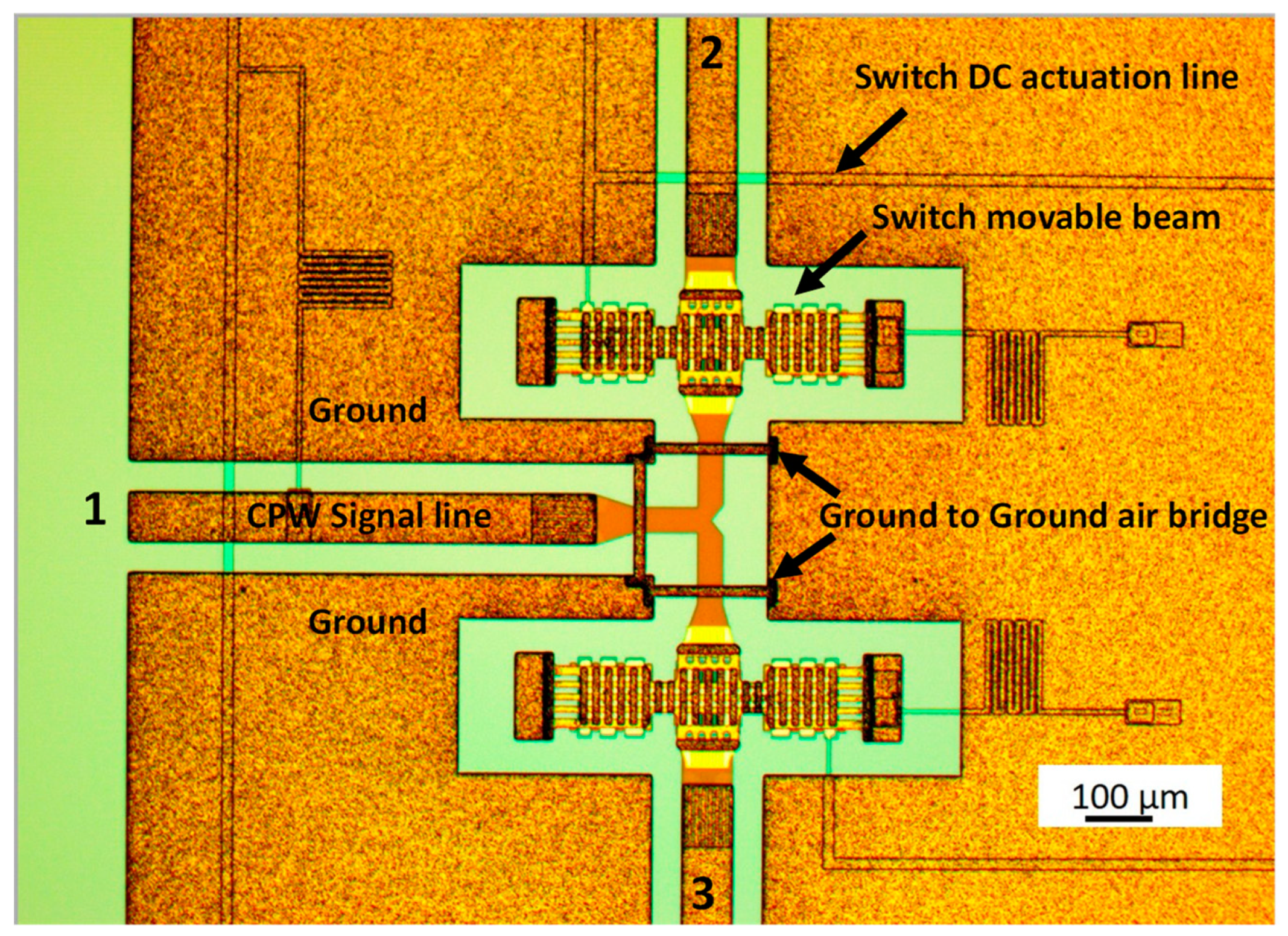
Two preliminary technological runs have been performed to select the more promising configuration for the SPDT switch. The final layout used in this work for the actual devices is shown in
Figure 1.
Two clamped-clamped microswitches are used to send the input signal from port 1 to port 2 or 3. The switch beam is made of gold with a thickness of about 1.8 µm for the flexible and deformable arms and about 5 µm for the rigid main body. The switches are electrostatically actuated using high-resistivity polysilicon electrodes underneath the lateral side of the beams. The air gap between the non-actuated switch, the underneath actuation electrodes, and the bottom signal line is 3 µm.
The main improvements between the first and the second run were the introduction of three air bridges, also pointed out in
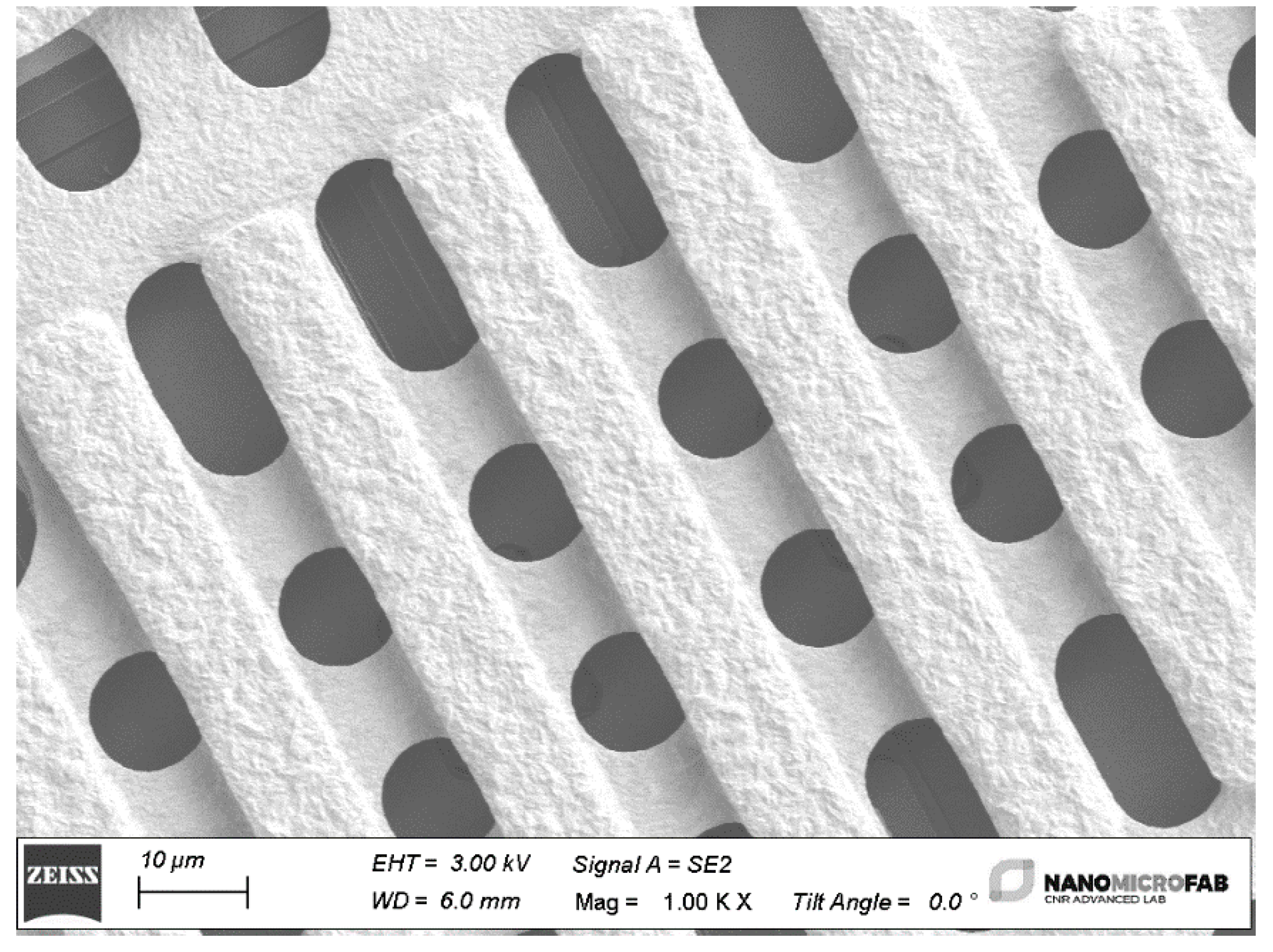
Figure 1, and a new configuration of the T-section, where the lines are tapered to provide a better impedance matching of the overall device. A section of the metal beam is shown in the SEM (scanning electron microscope) micrograph in
Figure 2, with particular attention to the holes necessary to remove the sacrificial layer below the bridge.
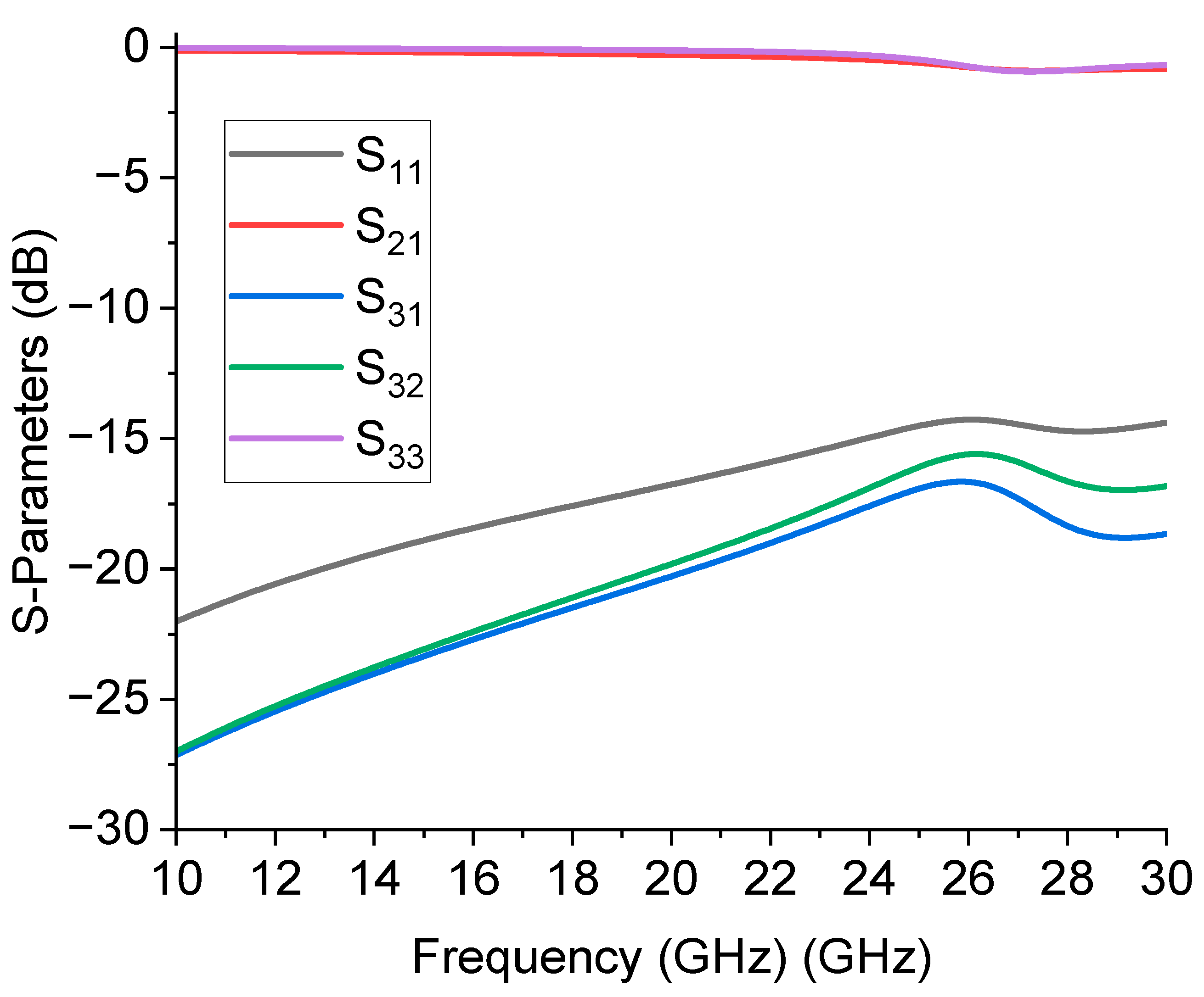
Considering all the geometrical details, a full-wave electromagnetic simulation has preliminarily verified this configuration. The results of the simulation, when the switch at port 3 is considered not actuated, are plotted in
Figure 3, in terms of matching at the input port (S
11), transmission to actuated branch (S
21), isolation between port 1 and 3, and between port 2 and 3, respectively S
31 and S
32. The reflections at the input port are below –20 dB until 25 GHz, then slowly degrades, but still acceptable up to 30 GHz (< -15 dB).
Regarding the transmission to port 2, in this case, the chosen active branch of the device, represented by the S21 parameter, shows an insertion loss above –1 dB. Finally, the isolations between disconnected ports, parameters S31 and S32, lie from –30 dB to –20 dB at the upper band, a pretty good value expected for the isolation, since it is obtained by one only not actuated switch.
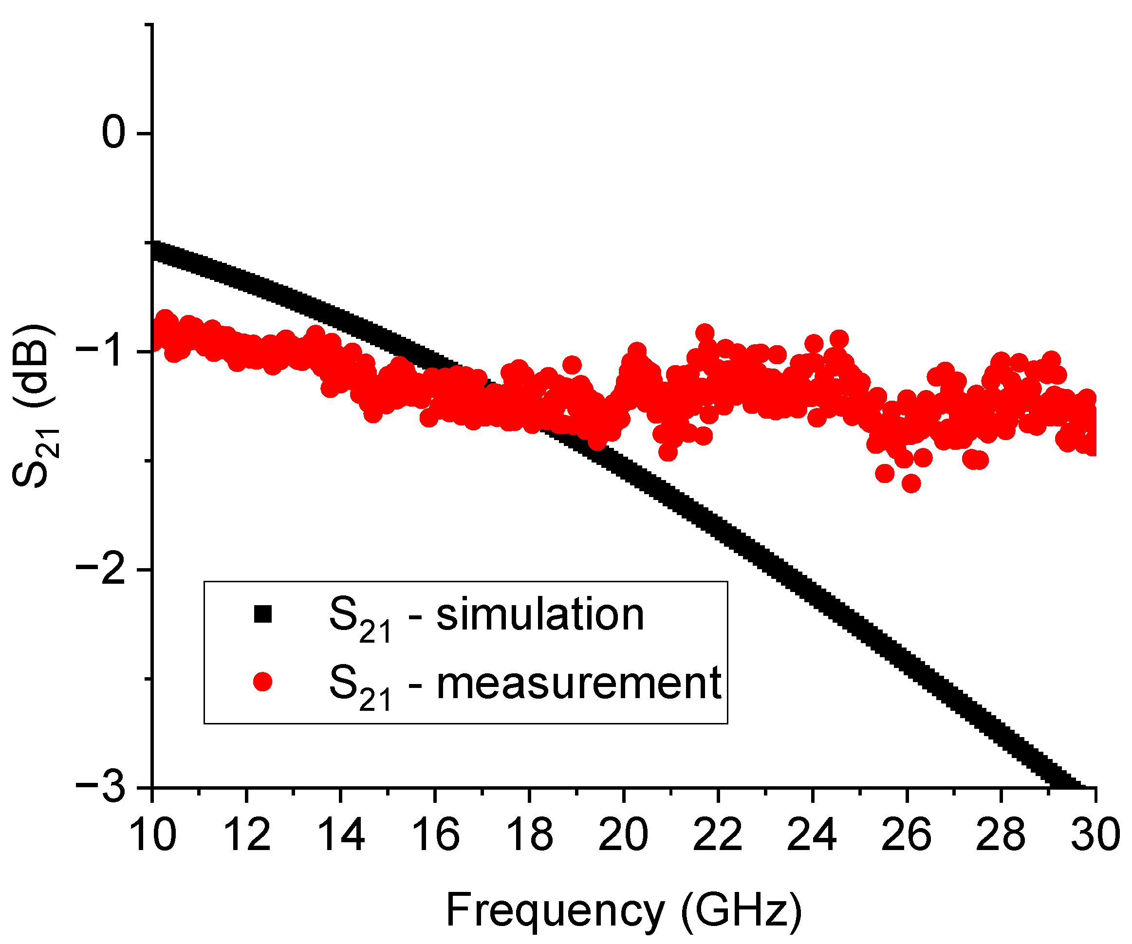
On the other hand, a complete analysis of this device should include a deformed bridge, electromechanically simulated to give a more realistic result. At the same time, most part of the simulations in the literature estimate the electrical response with a rigid ON-OFF functionality, moving the entire beam up or down with respect to the contact position. This gives under-estimated or over-estimated performance depending on the operative frequency because parasitic contributions cannot be correctly predicted. The situation is clarified in
Figure 4, where the simulation is compared with the experimental result for the transmission parameter S
21.
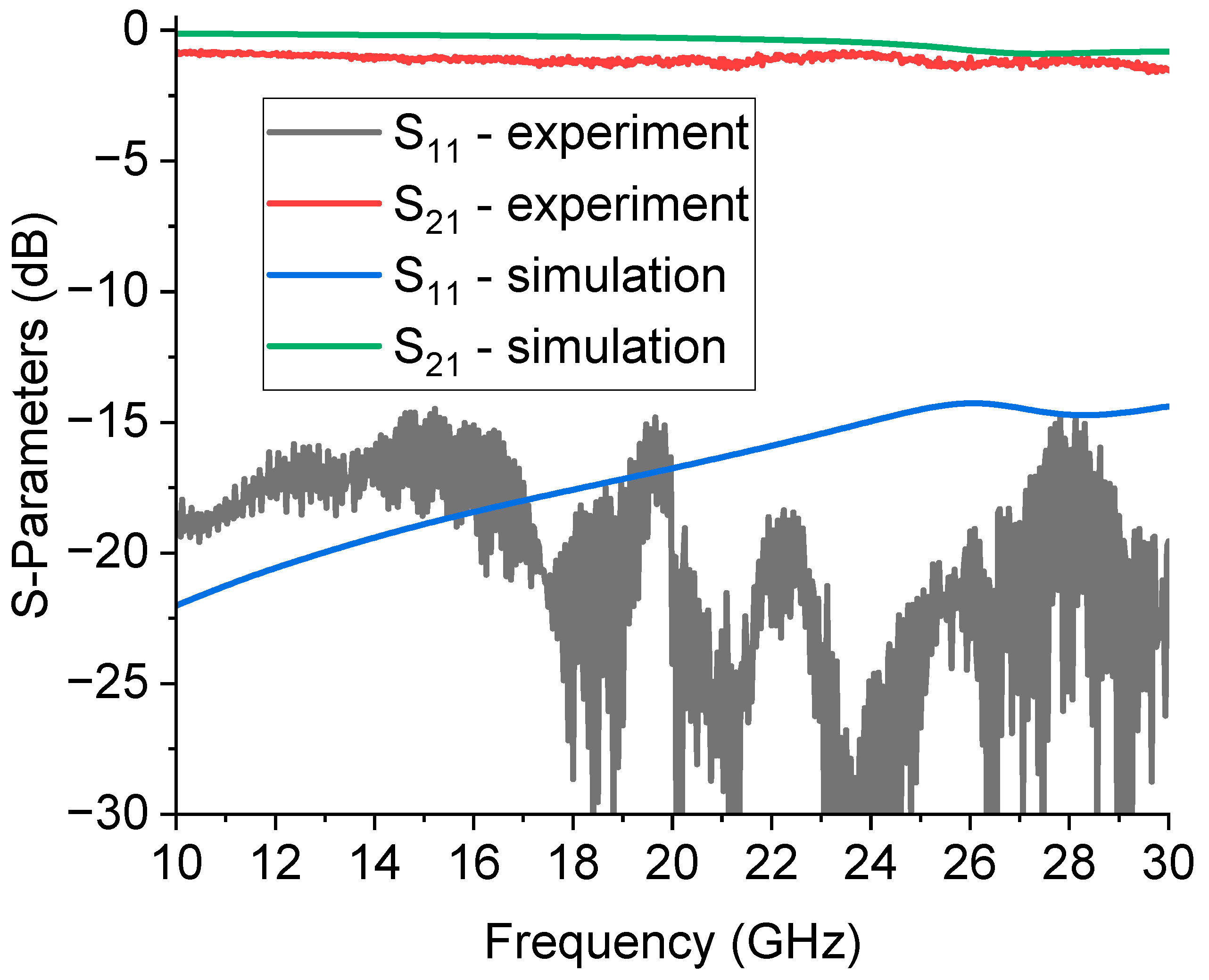
Good reflection and insertion loss performances have been obtained from an experimental point of view, as shown in the plot exhibiting the S
11 and S
21 parameters of the measured SPDT device in
Figure 5, compared with the simulation. As expected from an ohmic switch, a wideband response is also achieved.
The actuation voltage for the first actuation was relatively high, close to 80-90 V, but is reduced to 60-65 V after exercising the switch with more actuations, also contributing to removing some residuals after the etching of the sacrificial layer.
3. Sierpinski resonators
The triangular Sierpinski resonators have been considered for the advantages in tuning capability by fixing the footprint of the resonator and increasing the internal complexity, i.e., changing the number of sub-triangles starting from the original full metal patch. In addition, it is easy to combine them in multi-resonant structures, coupling a few resonators in non-conventional geometries. As anticipated in the introduction, it is also interesting to study this geometry from a fundamental point of view because a detailed theory of the resonant frequencies considering the CPW feeding of the resonators is not yet available for microwave signal processing. The resonators are fully embedded in a CPW boundary, and it is worth noting that this structure, as well as the U-shaped resonators discussed in the next section, is part of the more general family of metamaterial or fractal geometries corresponding to additional properties in the signal propagation. They are characterized by the exhibition of effective dielectric constant and magnetic permeability that are both negative, contributing to backward radiation for antennas and significant changes in the propagation properties for planar components. Results and comments about these properties in the studied geometries can be found in [
8] or in more general literature like [
9,
10,
11].
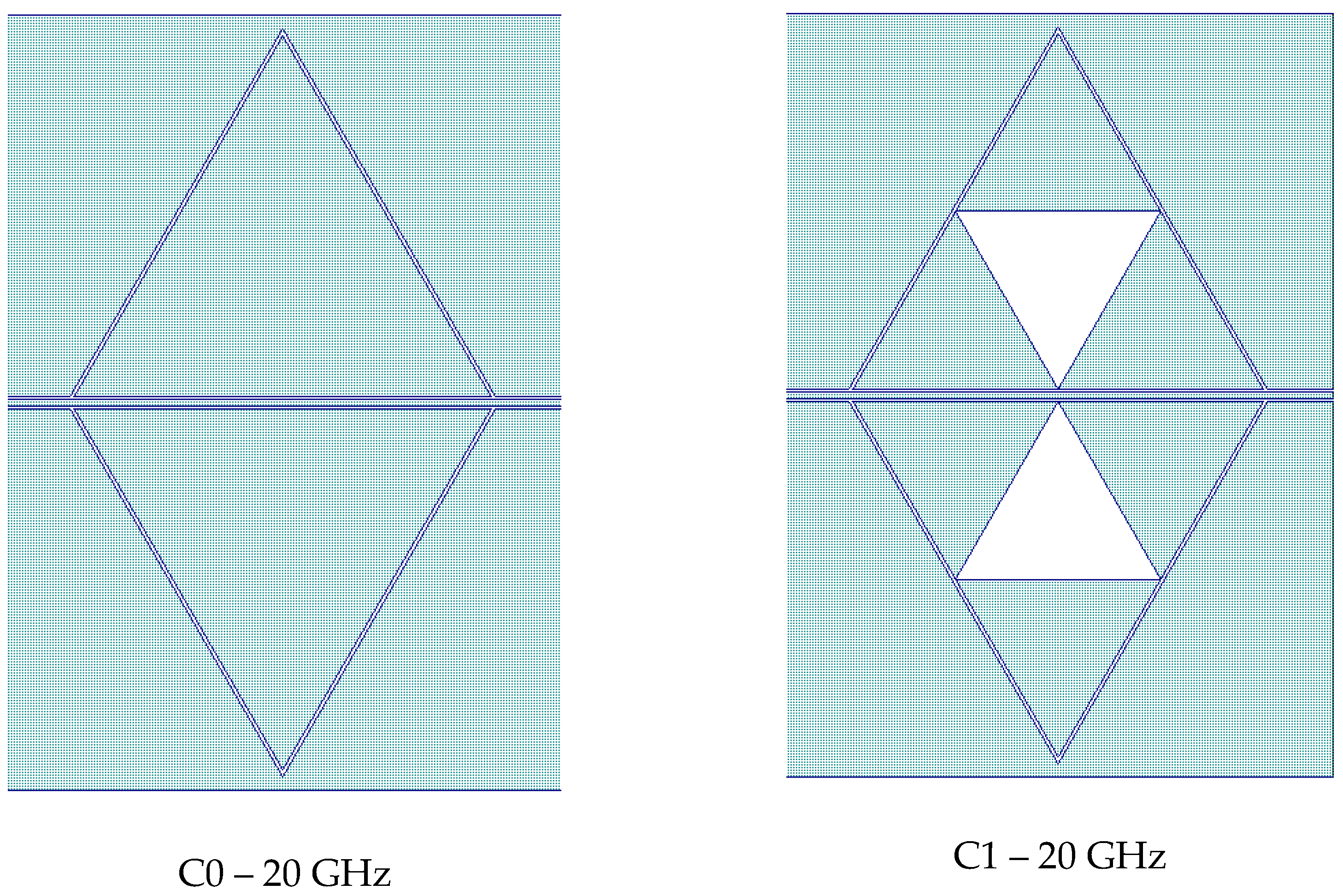
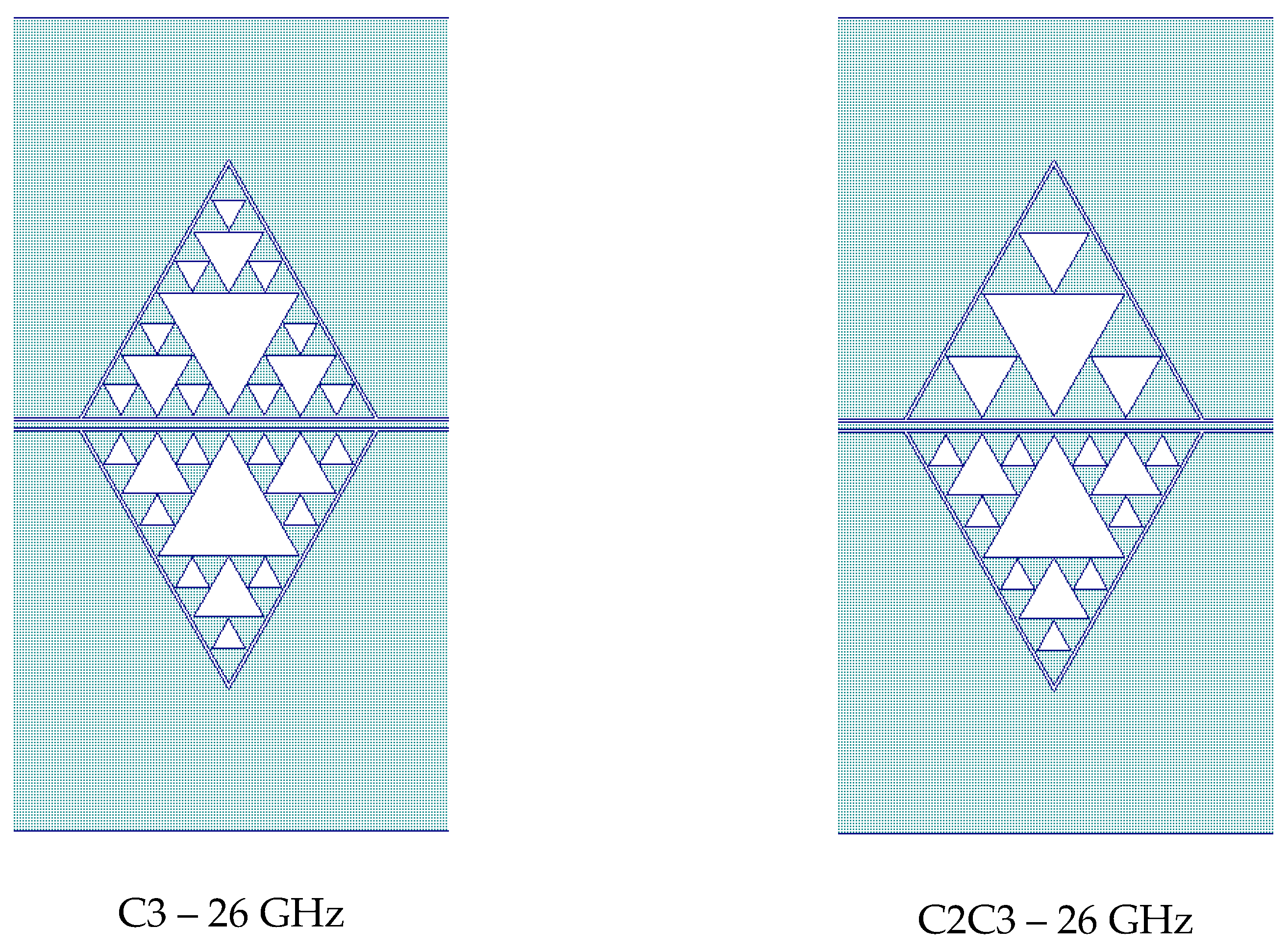
In our work, we have preliminarily studied a few triangular Sierpinski resonators and selected the configurations promising to filter adjacent frequencies for fine-tuning. Starting from the full triangular patch, we arrived at the third level of internal complexity determined by the number of sub-triangles, and we defined them C0, C1, C2, and C3. The single resonator performances are not necessarily the best choice when combining two or more geometries in a complex one. For this reason, after considering the results of the single resonators, we manufactured and tested for immediate purposes a structure including the C0 and C1 triangles, i.e., the entire patch and the first level of complexity for the Sierpinski structure working at 20 GHz. At the same time, the C3 and the C2C3 mixed configurations have been studied for the 26 GHz device. When we say “C2C3”, one of the triangles follows the C2 complexity, while the mirrored triangle is designed with the C3 geometry. The mirrored resonators in CPW configurations must have symmetric structures along the central conductor of the CPW and close to the ground boundaries to improve the electrical matching conditions. Primary considerations about the coupling issues and the spectrum reconstruction for CPW-fed Sierpinski structures have been discussed in [
8].
All the used configurations, including the mixed one, namely C2C3 for 26 GHz, are represented in
Figure 6. The difference in size is due to the two different working frequencies for the studied devices.
The individual response of the resonators has been already studied elsewhere [
8]. the approximated value of the wanted frequency of resonance has been obtained accounting for electromagnetic and experimental trials. Analytical tools are inadequate to predict resonance frequency because the past theory has been developed for via-hole or microstrip-fed antenna structures. The CPW environment embeds the resonators completely, and this will require a more complicated approach to derive the expected frequency of resonance analytically for the triangular patch and the Sierpinski triangles obtained with empty sub-triangles. So far, resonance frequencies close to the desired ones have been obtained with the help of electromagnetic simulations and experimental verifications. In this case, the length of the edge for the triangles was 4 mm and 6 mm, respectively, corresponding to resonances around 26 GHz and 20 GHz approx.
3.1. Results on the switched triangular 20 GHz resonators
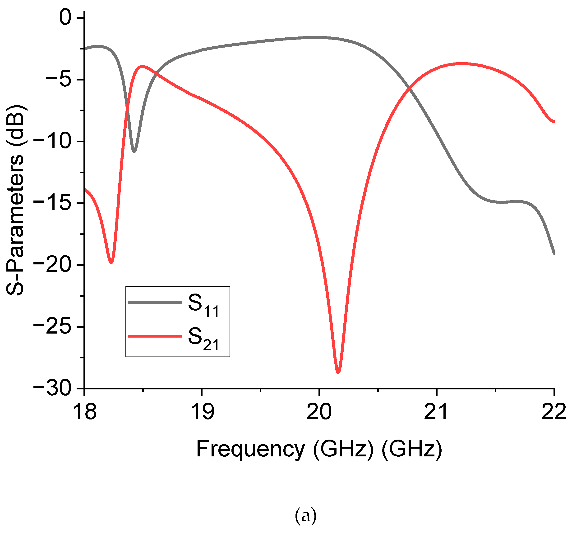
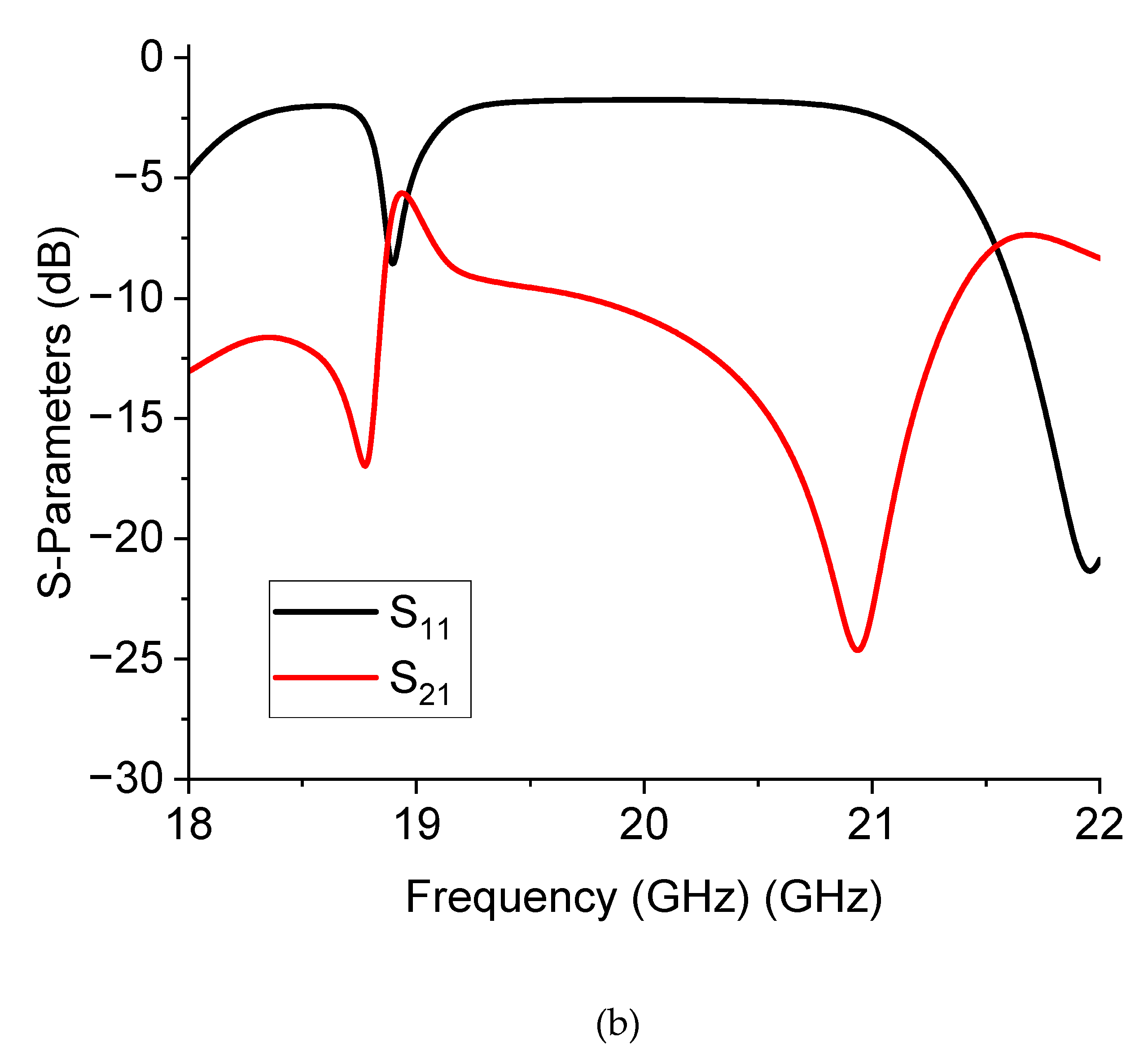
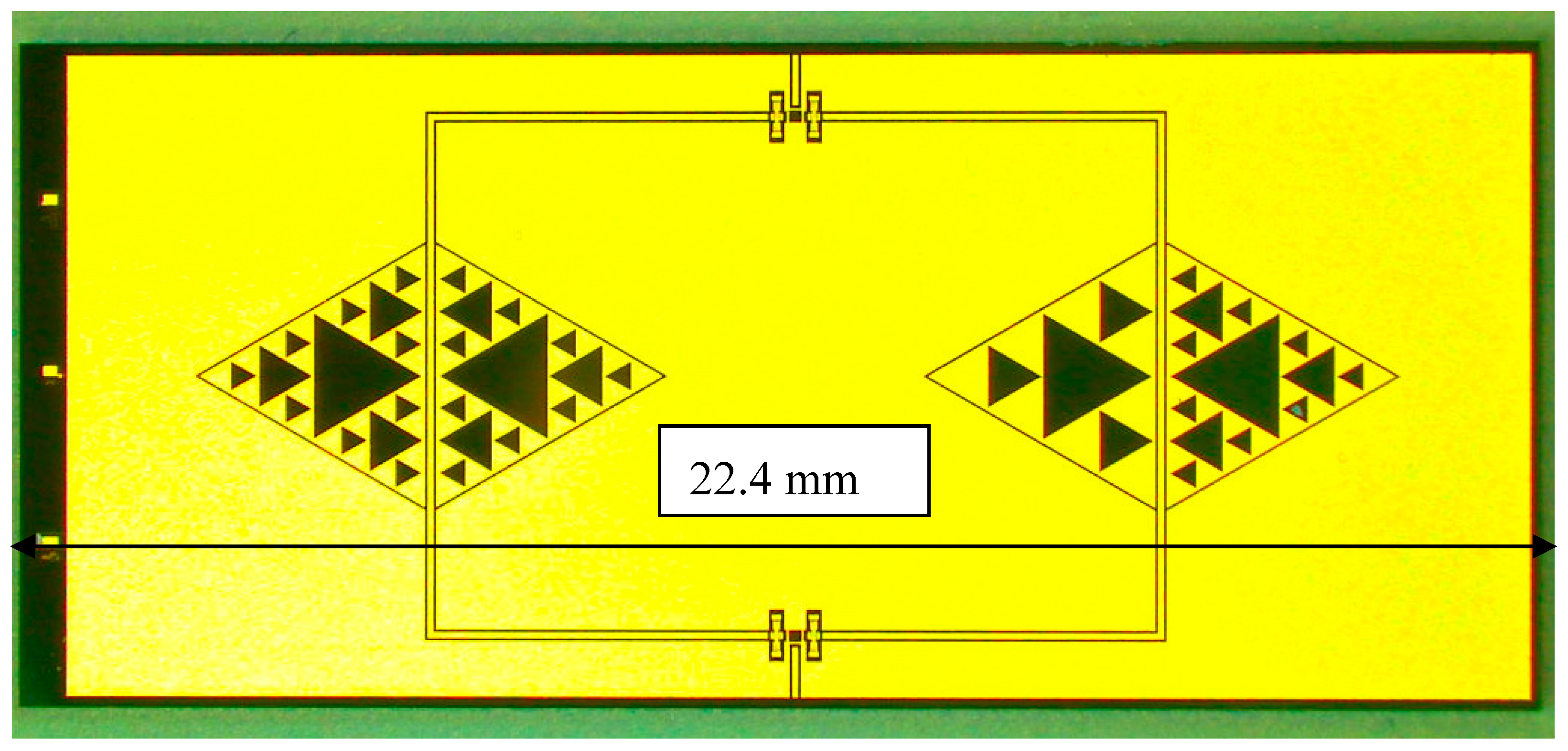
The results of the 20 GHz resonators, combining the C0 and C1 geometries, are presented in this section. The switched configuration is shown in
Figure 7, where the two possible states are given, considering an actuation on the filter's upper or lower branch, as shown in the figure. This configuration has been simulated to predict its response in the two possible states, and the simulation is presented in
Figure 8.
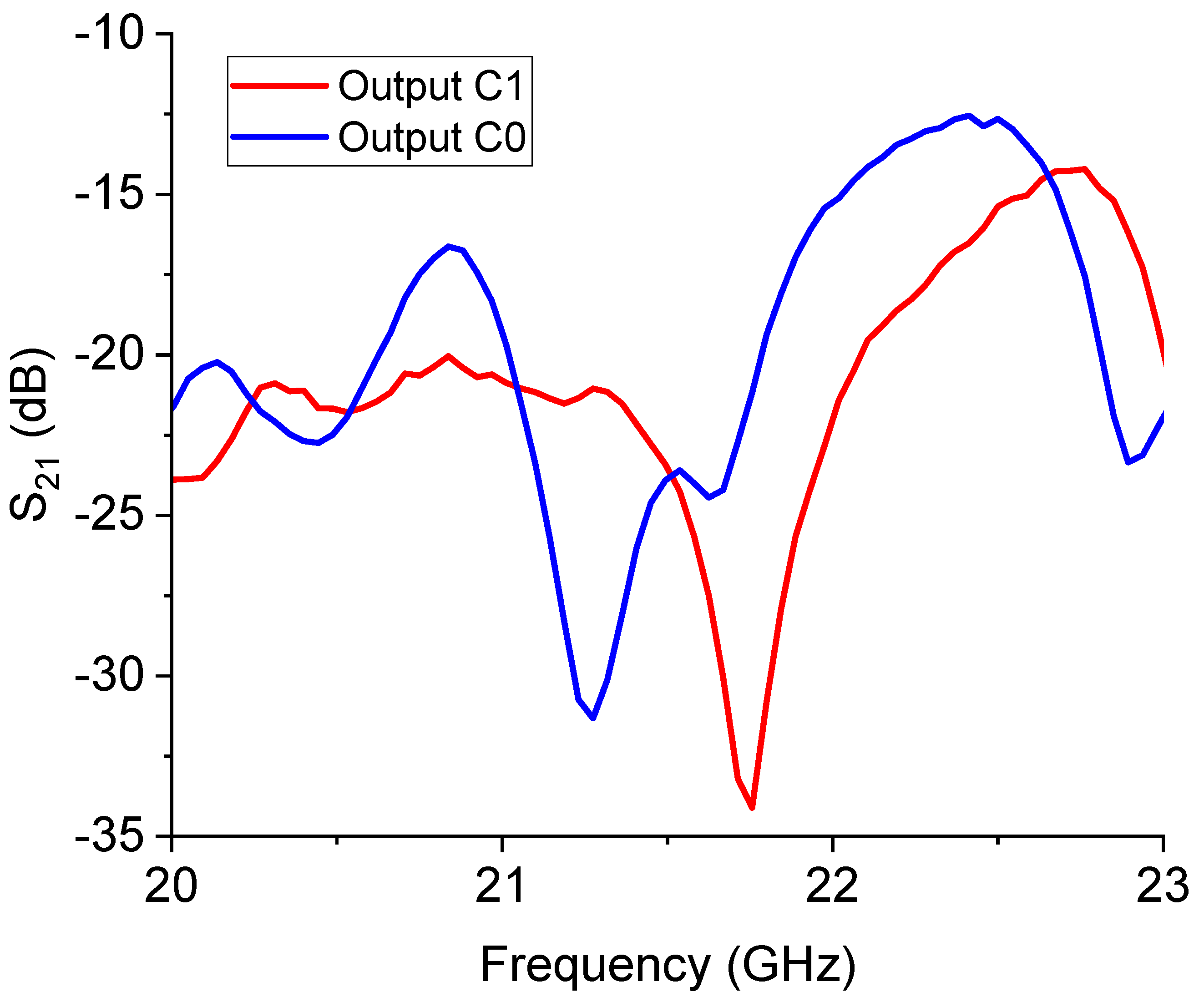
The experimental result for the transmission S21 parameter of this structure is shown in
Figure 9.
Despite the non-perfect matching causing significant losses along the line, the result agrees with the general expectations on this device, with a shift of the output resonance when the signal is switched from the C0 branch to the C1 one and a dynamic response for the ON/OFF states of the switch in the order of 15 dB at least. The predicted resonance frequency was around 20.16 GHz for the C0 response, while the measured one was 21.27 GHz; for the C1 output, the expected resonance lies at 20.93 GHz, while the measured one was 21.75 GHz. So, both frequencies are shifted by 1 GHz approx., and the difference between the two frequencies of resonance is 500 MHz and not 700 MHz as expected.
From the analysis of the obtained results, we can conclude that the big resonators working around 20 GHz probably interact between them in proximity to the internal corners. Better isolation could be provided by a post of absorbing material separating the two devices transversally or shifting the relative position to avoid interference due to the proximity between the corners of the triangles. The situation must also be improved at the I/O ports of the entire device to decrease the insertion losses significantly. So far, the proof-of-concept is demonstrated at this stage, but the complete device needs to be correctly engineered for application purposes.
3.2. 26 GHz switched triangular resonators. Design and test.
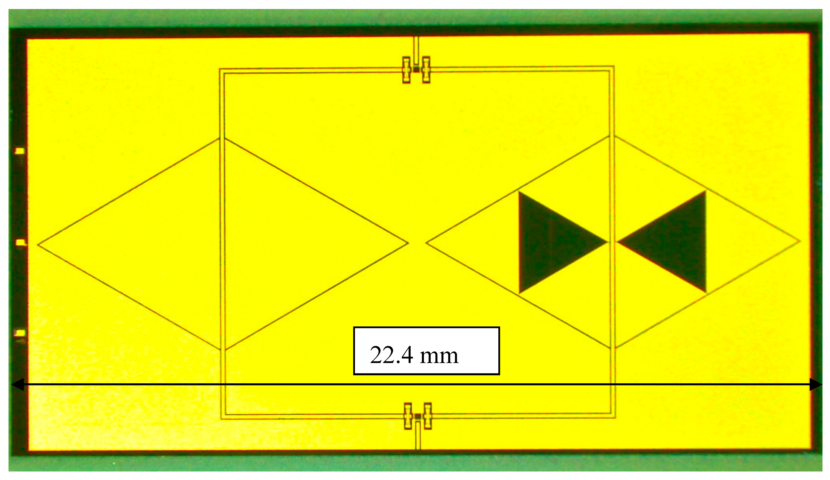
The nominal 26 GHz switched resonator configuration is shown in the layout of
Figure 10. In this case, a C3 configuration represents the left branch of the filter, while the C2C3 structure is on the right side.
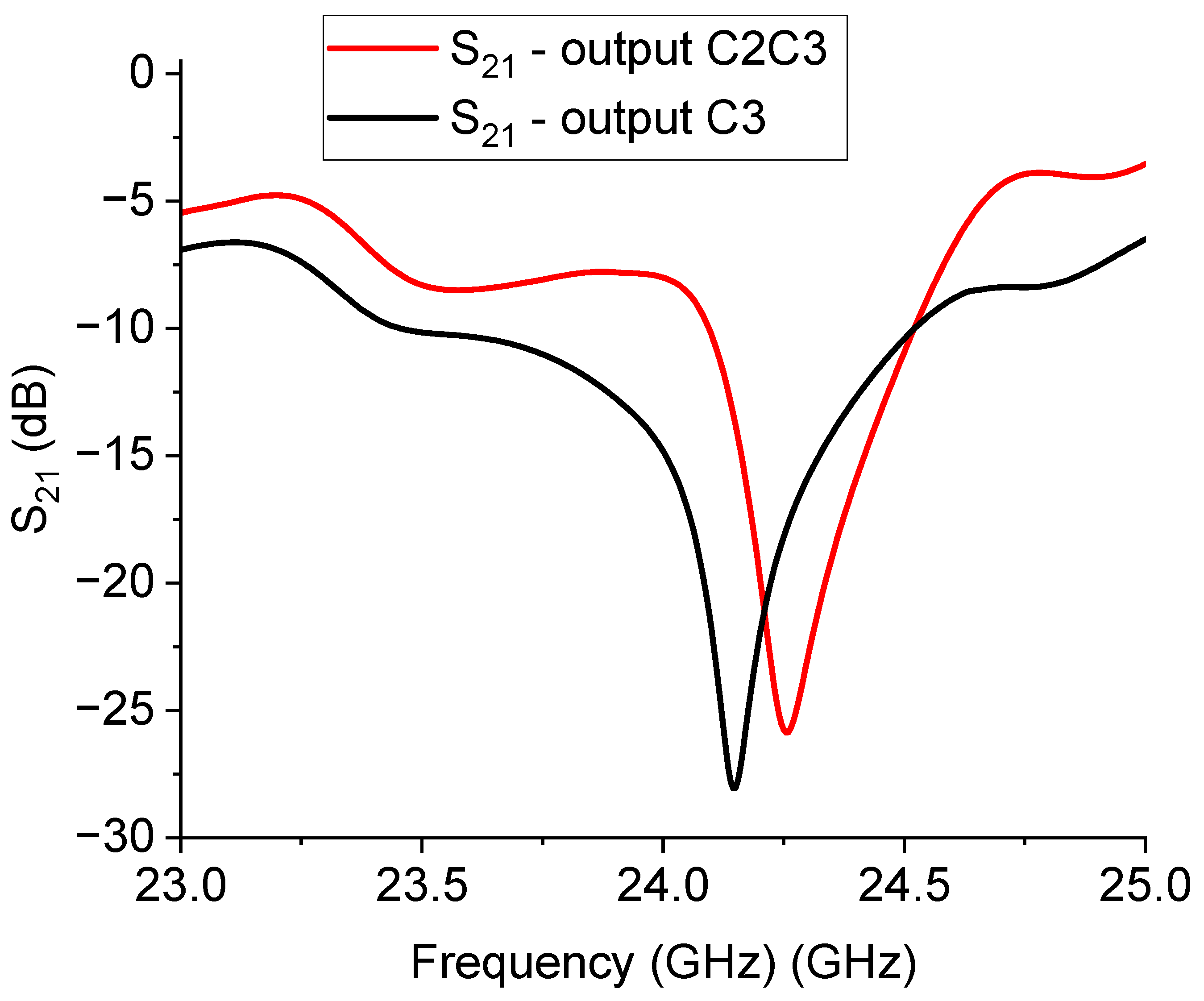
The expected response for the 26 GHz filtering is shown in
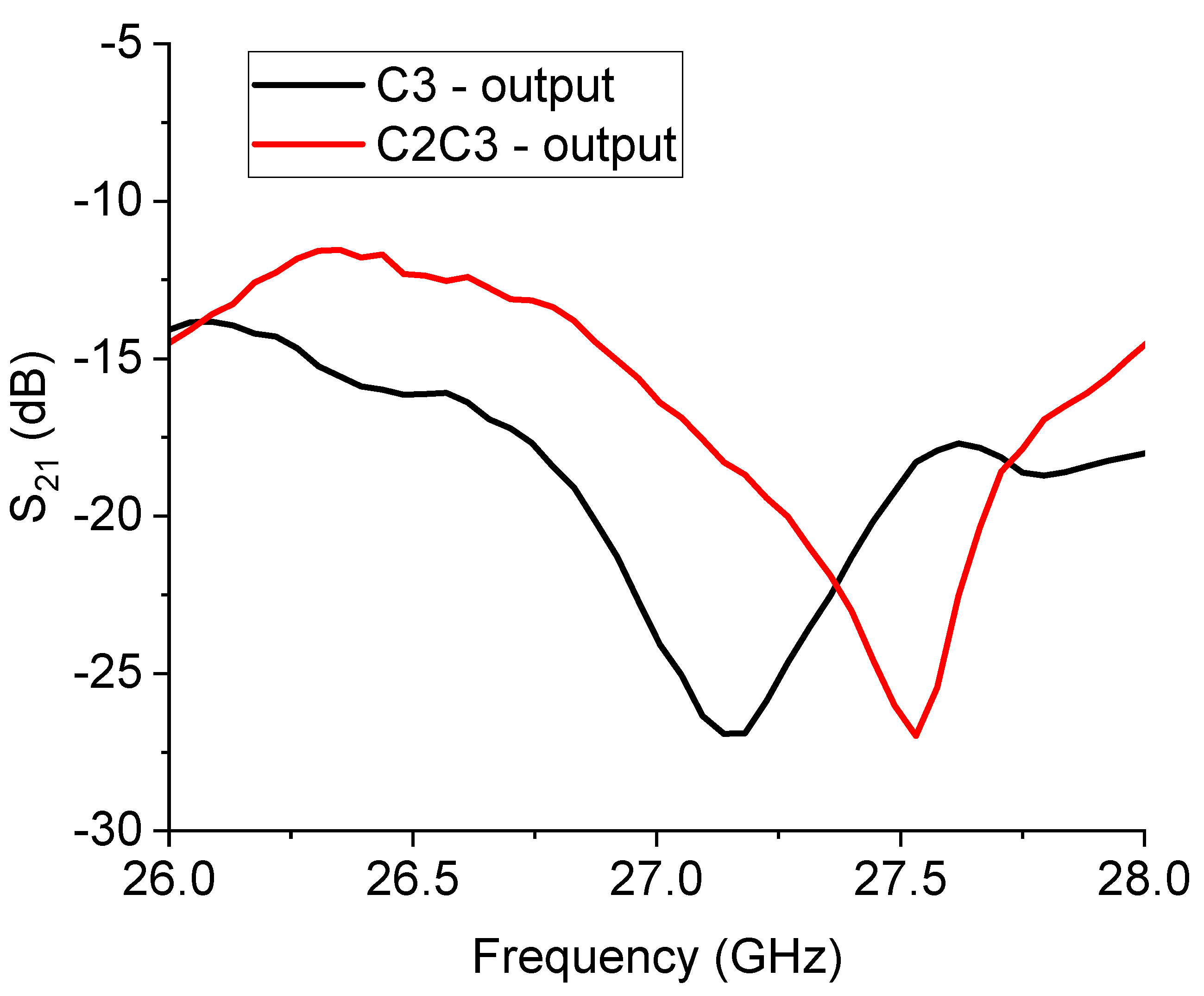
Figure 11, while the measured performance is given in
Figure 12.
Looking at the experimental results, like in the case of the switched 20 GHz triangles, it is worth noting the necessity to improve the I/O coupling for engineering purposes. On the other hand, a dynamic ON/OFF response of the primary mode is obtained with approximately 15 dB of rejection. Nevertheless, a frequency shift of the main mode up to approx. 27 GHz. must be accounted for. In detail, the expected resonance for the entire structure was 24.14 GHz for the C3 output and 24.25 GHz for the C2C3 output, while the experimental response was 27.13 GHz and 27.53 GHz for the C3 and C2C3 output, respectively. It must be stressed that the design is strongly affected by a shift with respect to the chosen resonance frequency, and this is particularly evident when the wanted resonance frequency is higher, beginning to be closer to the millimeter wave range. Such an effect is probably due to the necessity of an improved simulation effort on the entire structure, involving more geometrical details and specific characterization of the employed materials, which can contribute to the equivalent circuit modifying the spectrum in a non-negligible way. While the preliminarily studied single resonators exhibited resonance frequencies closer to the wanted one, the entire structure, including the SPDT and the feeding lines and discontinuities (like the bending on the corners), shows significant differences compared to the original design goals. In this case, smaller resonators help to have a decreased interaction, even if, also for this configuration, a shift in the position of the resonators could be helpful for more effective isolation between the two states.
4. U-shaped resonators
Until now, U-shaped resonators have been studied mainly in microstrip configurations for filtering applications or combined in arrays for antenna and high-frequency absorber purposes. The U-resonator alone is not necessarily suitable for a metamaterial response, at least the resonators studied in [
8]. Still, their collective excitation is usually referred to as a metamaterial-inspired structure. The main advantage of a U-shape in filtering applications is the possibility of bending a resonating line with a consequent decrease in the footprint. This solution allows a designer to use the U-elements in the well-established coupled-line filters designed in microstrip configuration, substituting straight lines with bent ones. A well-known example of using U-bended lines is the hairpin filter [
13,
14]. Preliminary work on filters implemented by RF MEMS switches has been performed in [
12]. The drawback of the line-bending procedure is to account during the design of the device for the discontinuity created by the bending itself, whose equivalent circuit modifies the resonant frequency. Another delicate point to be considered is the coupling between the resonator and the feeding line, either a microstrip or a CPW.
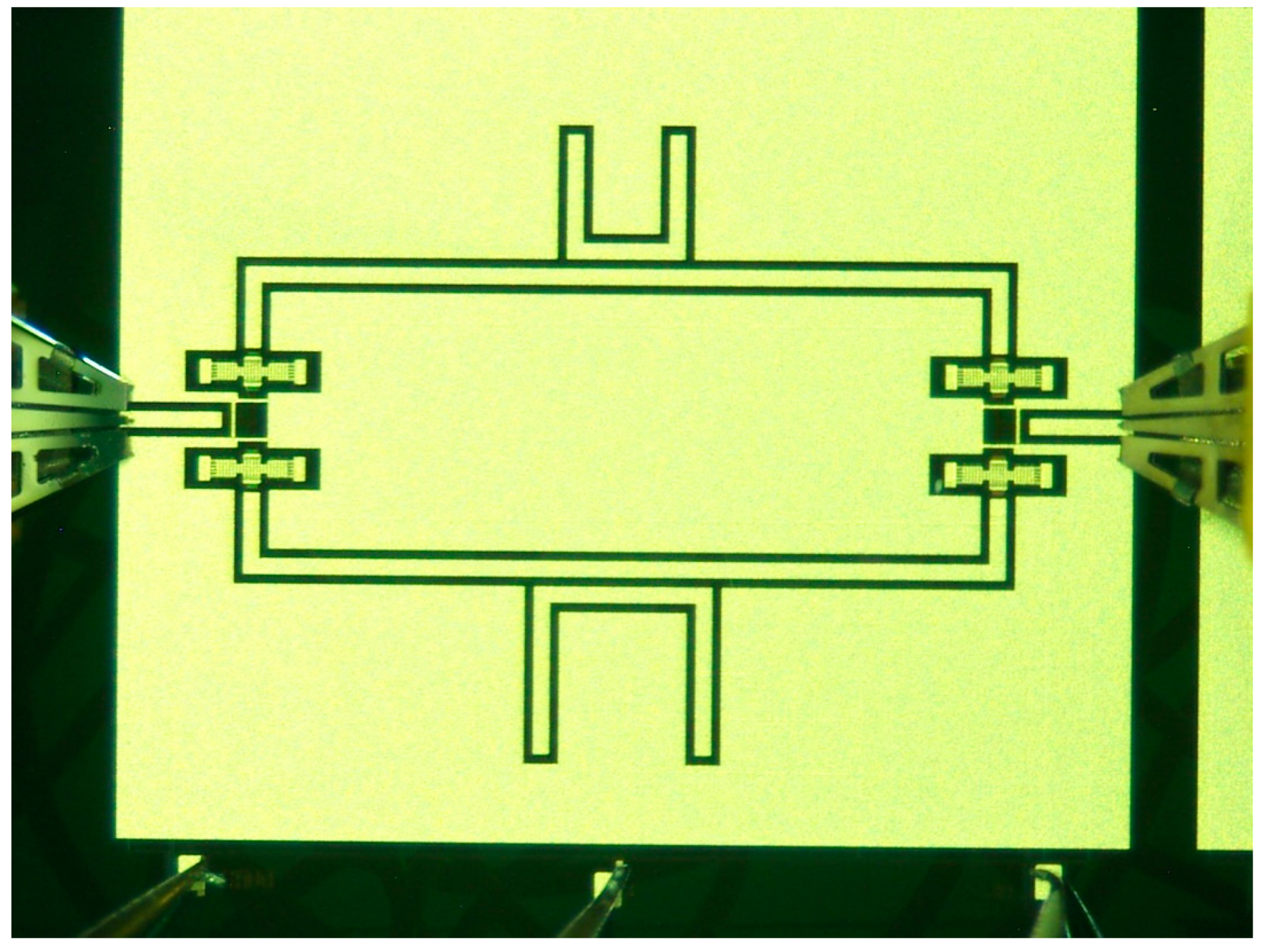
The structures studied in this paper combine a 20 GHz resonator and a 26 GHz resonator coupled to the central conductor of a CPW and placed on two branches separated by an SPDT RF MEMS switch. The SPDT drives the signal on the branch selected by the actuation of the corresponding membrane. In the following
Figure 13, the configuration used for the double frequency filter is shown during an on-wafer measurement.
In
Figure 14, the predicted performance of the switched filter based on the U-resonators is shown, where the selected frequencies around 20 GHz and 26 GHz result from the simulation of the individual filter response. As previously discussed, additional resonances can appear in the spectrum, but having a series of resonances is intrinsic to the nature of all the resonators, depending upon the size of the resonators, and corrected by their effective lengths because of electromagnetic boundary effects and the coupling conditions. The main mode is almost correctly predicted at 20 GHz; the same happens for the 26 GHz resonator.
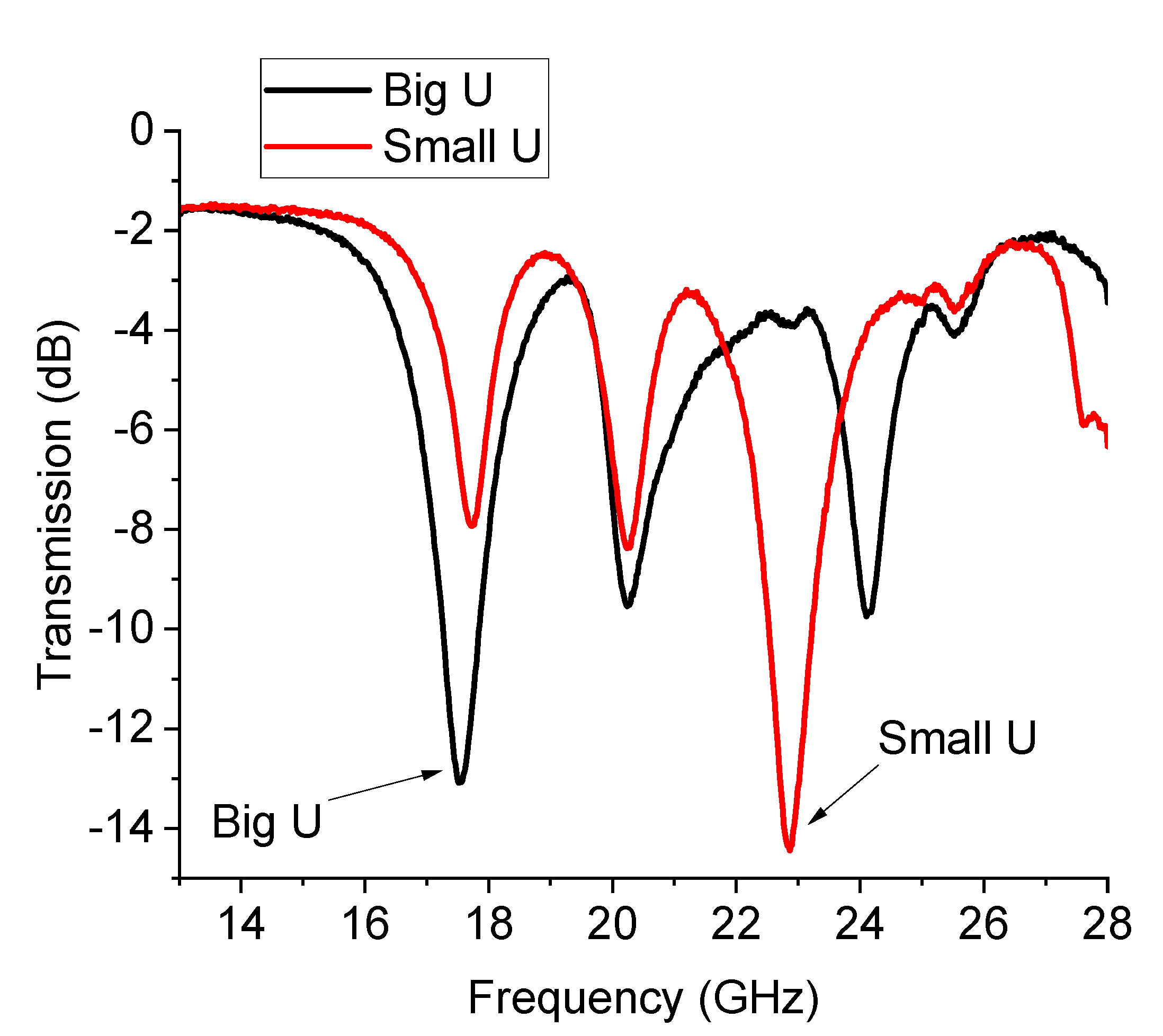
Experimentally, the situation is more complicated. The presence of the switches and the feeding lines, together with the intrinsic nature of the resonators of being multi-resonant, allow the excitation of multiple peaks because a non-perfect matching or unwanted inhomogeneities create discontinuities that can excite higher order modes, thus hindrance the possible selection of two single resonances. This situation is clearly shown in
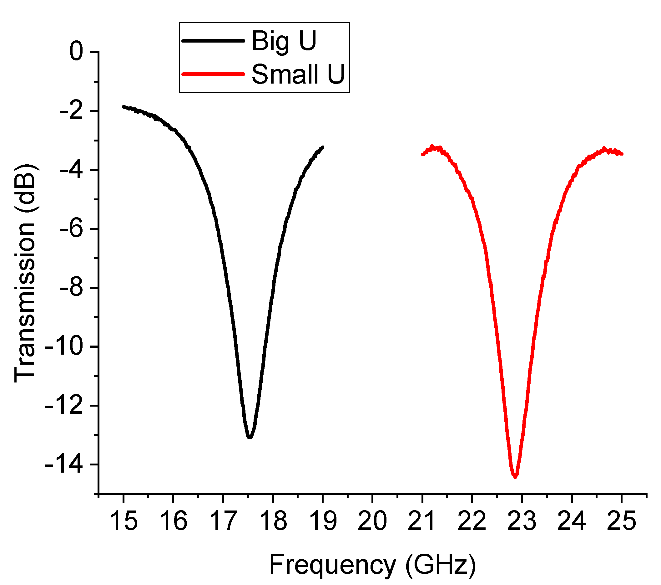
Figure 15, where the measured response of the U-structures is plotted. An arrow has been used to indicate the main resonance due to the single resonator (big or small) activated by the branch selected using the SPDT. Like in the case of the already discussed triangles, a further improvement of this configuration should include a shift in the position of the two individual resonators to have better physical separation and to mitigate the possible interaction between them. Additionally, both the main resonance modes are shifted with respect to the expected single resonances because of the influence of the entire network. For clarity, the main modes have been isolated from the previous figure and plotted separately in
Figure 16.
In
Figure 16, the almost full correctness in the expected difference between the frequency of resonance of the small resonator and the big one is highlighted, even if the spectrum is shifted downwards. The expected frequencies for both resonators were 19.8 GHz and 26.02 GHz (from
Figure 14), while the experimental ones are 17.52 GHz and 22.82 GHz (from
Figure 15). So far, a downward shift of approx. 2 GHz has been experienced while comparing theory and experiment.
In conclusion, the studied resonators are promising as individual devices. Still, a better selection is needed, accounting for the multi-resonant response of the entire structure and the shift induced by the influence of all the circuital components.
5. Conclusions
This paper proposes switched triangular and U-shaped band-stop resonators implemented by MEMS technology, employing an RF MEMS SPDT to select the path for the RF output. The individual resonators are: (i) Sierpinski-based triangular structures obtained by increasing the internal complexity of a full metal patch using empty internal sub-triangles and (ii) U-shaped structures. Both switched resonators have been designed in CPW configurations and are suitable for more complex structures involving coupled individual resonators. Devices working at 20 GHz and 26 GHz have been studied for potential K-Band operation, proving promising performances and suitable optimizations. The best results are obtained when the resonators are far enough from each other to prevent an unwanted interaction, especially among the big ones working at lower frequencies. A further engineering step is necessary to improve the insertion losses of the full devices, although the basic requirements to select two different frequencies have been demonstrated by a rejection ratio of nearly 15 dB between the ON/OFF states of the switches.
Author Contributions
Contributions from the Authors were the following: Technology and Program co-Management, Flavio Giacomozzi; Layout Design and Participation to Technology: Emanuela Proietti, Giovanni Capoccia, Jacopo Iannacci, Girolamo Tagliapietra; Design and Test: Giovanni Maria Sardi; Funding Acquisition, Device Design and Measurement, Romolo Marcelli.
Funding
Cofunded by the Italian Space Agency Project «METAMEMS», Grant No. ASI n. 2019-12-U.0 - bando di finanziamento di progetti di ricerca industriale e/o sperimentale ‘Nuove Idee per la Componentistica Spaziale del Futuro (“TRL”)’, Codice Unico di Progetto (CUP) F84118000380005.
Data Availability Statement
Raw data available upon requirement.
Conflicts of Interest
The authors declare no conflict of interest.
References
- F. Souchon, D. F. Souchon, D. Saint-Patrice, J. L. Pornin, D. Bouchu, C. Baret and B. Reig, "Thin film packaged redundancy RF MEMS switches for space applications," 2017 19th International Conference on Solid-State Sensors, Actuators and Microsystems (TRANSDUCERS), 2017, pp. 175-178. [CrossRef]
- Andrea Lucibello, Romolo Marcelli, Emanuela Proietti, Giancarlo Bartolucci, Viviana Mulloni, Benno Margesin, Reliability of RF MEMS capacitive and ohmic switches for space redundancy configurations; Microsystem TechnologiesVolume 21Issue 9September 2015 pp 1903–1913. [CrossRef]
- Nardo, S.D. Nardo, S.D., Farinelli, P., Kim, T., Marcelli, R., Margesin, B., Paola, E.D., Pochesci, D., Vietzorreck, L., & Vitulli, F. (2013). Design of RF MEMS based switch matrix for space applications. Advances in Radio Science, 11, 143-152. [CrossRef]
- Sinha, S. Sinha, S., Bansal, D. & Rangra, K. (2012). RF MEMS compact T-type switch design for switch matrix applications in space telecommunication. IEEE-International Conference on Advances in Engineering, Science and Management, ICAESM-2012:130–135.
- Weiwei Zhou, Wexing Sheng, Jie Cui, Yubing Han, Xiaofeng Ma, Renli Zhang, SR-Crossbar topology for large-scale RF MEMS switch matrices IET Microw. Antennas Propag., 2019, Vol. 13 Iss. 2, pp. 231-238. [CrossRef]
- https://www.memsjournal.com/2021/11/rf-mems-maker-sofant-technologies-signs-82-million-contract-with-european-space-agency.html#more.
- Shi, Y.; Shen, Z. Shi, Y.; Shen, Z. Recent Advances in Flexible RF MEMS. Micromachines 2022, 13, 1088. [CrossRef]
- R. Marcelli, G. R. Marcelli, G. Capoccia, G.M. Sardi, G. Bartolucci, B. Margesin, J. Iannacci, G. Tagliapietra, F. Giacomozzi, E. Proietti, Metamaterials based RF microsystems for telecommunication applications, Ceramics International. [CrossRef]
- Christophe Caloz, Tatsuo Itoh, Electromagnetic Metamaterials: Transmission Line Theory and Microwave Applications, ISBN: 978-0-471-66985-2 November 2005 Wiley-IEEE Press 376 Pages.
- Tie Jun Cui, David Smith, Ruopeng Liu (Editors), Metamaterials - Theory, Design, and Applications, Springer-Verlag US 2010. [CrossRef]
- Filippo Capolino, Theory and Phenomena of Metamaterials, CRC Press, 19 dic 2017 - 974 pagine.
- Donelli, M.; Manekiya, M.; Tagliapietra, G.; Iannacci, J. Donelli, M.; Manekiya, M.; Tagliapietra, G.; Iannacci, J. A Reconfigurable Pseudohairpin Filter Based on MEMS Switches. Sensors 2022, 22, 9644. [CrossRef]
- Sheng-Yuan Lee, and Chih-Ming Tsai, New Cross-Coupled Filter Design Using Improved Hairpin Resonators, IEEE TRANSACTIONS ON MICROWAVE THEORY AND TECHNIQUES, VOL. 48, NO. 12, DECEMBER 2000, pp.2482-2490. [CrossRef]
- Yingjie Di, Peter Gardner, Peter S. Hall, H. Ghafouri-Shiraz, and Jiafeng Zhou, Multiple-Coupled Microstrip Hairpin-Resonator Filter, IEEE MICROWAVE AND WIRELESS COMPONENTS LETTERS, VOL. 13, NO. 12, DECEMBER 2003, pp.532-534. [CrossRef]
Figure 1.
Manufactured SPDT switch. The arrows point to the actual details of the device, including the air bridges’ location with the optimized geometry of the T-junction, the individual switches, the actuation lines and the CPW feeding line.
Figure 1.
Manufactured SPDT switch. The arrows point to the actual details of the device, including the air bridges’ location with the optimized geometry of the T-junction, the individual switches, the actuation lines and the CPW feeding line.
Figure 2.
SEM micrograph with detail of the metal beam layout. In this section, the metal beam has been reinforced with a double-step electroplating process to strengthen the central part mechanically, closing the interrupted central conductor of the CPW. In contrast, only a single-step electroplating has been performed on the anchors to maintain an elastic response during the actuation. As usual, the holes facilitate removing the sacrificial layer underneath the bridge.
Figure 3.
Simulated results of the SPDT configuration when the switch at port 3 is considered not actuated. Results are reported in terms of matching at the input port (S11), transmission to actuated branch (S21), isolation between ports 1 and 3 and ports 2 and 3 (S31 and S32, respectively), and reflection from port 3 (S33).
Figure 4.
Comparison between the expected S21 parameter, in dB scale, for the SPDT configuration used in this work. The losses are underestimated below 20 GHz and overestimated above. On the other hand, an acceptable loss level has been obtained for the entire device transmission performance, comparable with the same configurations studied in the literature.
Figure 5.
Experimental response of the RF MEMS SPDT. Reflection (S11) and Transmission (S21) response, with port 3 in isolation.
Figure 5.
Experimental response of the RF MEMS SPDT. Reflection (S11) and Transmission (S21) response, with port 3 in isolation.
Figure 6.
Resonator configurations are used for the 20 GHz and 26 GHz operation. The length of the edge of the individual triangles is 4 mm for the 26 GHz, and 6 mm for the 20 GHz operation, respectively.
Figure 6.
Resonator configurations are used for the 20 GHz and 26 GHz operation. The length of the edge of the individual triangles is 4 mm for the 26 GHz, and 6 mm for the 20 GHz operation, respectively.
Figure 7.
Layout of the switched C0 and C1 resonators for the 20 GHz operation. The RF MEMS switches are evidenced on the upper and bottom sides of the figure to allow the signal to pass through the C0 or the C1 resonator, depending on the actuated branch.
Figure 7.
Layout of the switched C0 and C1 resonators for the 20 GHz operation. The RF MEMS switches are evidenced on the upper and bottom sides of the figure to allow the signal to pass through the C0 or the C1 resonator, depending on the actuated branch.
Figure 8.
Simulation of the two-port filter implemented with the resonators C0 and C1 for the 20 GHz operation. In (a) the C0 configuration is activated, while in (b) the C1 resonator has been used as the output of the SPDT driven structure.
Figure 8.
Simulation of the two-port filter implemented with the resonators C0 and C1 for the 20 GHz operation. In (a) the C0 configuration is activated, while in (b) the C1 resonator has been used as the output of the SPDT driven structure.
Figure 9.
Experimental response for the 20 GHz switched filter with the C0 and C1 triangles.
Figure 9.
Experimental response for the 20 GHz switched filter with the C0 and C1 triangles.
Figure 10.
C3-C2C3 switched resonator for the 26 GHz operation. The same criterion is used with respect to the 20 GHz resonators, with the SPDT driving the output signal through the C3 (left side) or the C2C3 (right side) structure depending on the actuated branch.
Figure 10.
C3-C2C3 switched resonator for the 26 GHz operation. The same criterion is used with respect to the 20 GHz resonators, with the SPDT driving the output signal through the C3 (left side) or the C2C3 (right side) structure depending on the actuated branch.
Figure 11.
Simulation of the C2C3 structure for the 26 GHz filtering.
Figure 11.
Simulation of the C2C3 structure for the 26 GHz filtering.
Figure 12.
Measure of the 26 GHz filter performance.
Figure 12.
Measure of the 26 GHz filter performance.
Figure 13.
Layout of the U-switched resonators. In this picture, the upper resonator allows the 26 GHz output, while the 20 GHz resonator is shown on the bottom side.
Figure 13.
Layout of the U-switched resonators. In this picture, the upper resonator allows the 26 GHz output, while the 20 GHz resonator is shown on the bottom side.
Figure 14.
Expected resonances for the structure with two U-shaped resonators working at 20 GHz and 26 GHz, respectively.
Figure 14.
Expected resonances for the structure with two U-shaped resonators working at 20 GHz and 26 GHz, respectively.
Figure 15.
Resonance response for the switched U-resonators. A multi-resonant behavior is recorded. Evidence is given for the activation of the big and small resonators, originally designed for the 20 GHz and 26 GHz operation.
Figure 15.
Resonance response for the switched U-resonators. A multi-resonant behavior is recorded. Evidence is given for the activation of the big and small resonators, originally designed for the 20 GHz and 26 GHz operation.
Figure 16.
Detail of the main resonance for the big and small U-resonators. A significant shift is obtained with respect to the individual filters.
Figure 16.
Detail of the main resonance for the big and small U-resonators. A significant shift is obtained with respect to the individual filters.
|
Disclaimer/Publisher’s Note: The statements, opinions and data contained in all publications are solely those of the individual author(s) and contributor(s) and not of MDPI and/or the editor(s). MDPI and/or the editor(s) disclaim responsibility for any injury to people or property resulting from any ideas, methods, instructions or products referred to in the content. |
© 2023 by the authors. Licensee MDPI, Basel, Switzerland. This article is an open access article distributed under the terms and conditions of the Creative Commons Attribution (CC BY) license (http://creativecommons.org/licenses/by/4.0/).
