1. Introduction
Multi-junction solar cells comprised of stacked semiconductor p-n junctions tuned to different bandgaps represent the highest-efficiency photovoltaic technology, with recent demonstrations exceeding 47% efficiency [
1]. However, optimizing the design and layer thicknesses of multi-junction architectures is extremely challenging due to the complex interdependencies between optical absorption, carrier transport, lattice matching, and materials integration [
2].
Precisely balancing these optical and electronic properties is critical for maximizing the performance of each junction and the overall cell. But the high-dimensional design space makes intuition-based trial-and-error experimental iteration intractable. This leads to sub-optimal thicknesses and doping levels, limiting efficiency [
6].
Previous multi-junction optimization efforts relied on experimental fabrication processes to incrementally vary layer dimensions [
3]. But the tremendous time and resource costs of this approach did not systematically explore interactions between the numerous layered semiconductors. Genetic algorithms and global optimizers have also been applied, but often without rigorous statistical model validation [
4].
This work addresses the need for data-driven design guidelines to efficiently navigate the complex multi-junction design space. Our methodology leverages predictive modeling on statistically partitioned data and validated device simulations to uncover optimized thicknesses [
5]. This framework provides a pathway to push beyond existing single-junction records through methodical multi-junction optimization.
We specifically enhance the efficiency of a 5-junction III-V cell from 26% to over 47% under 1 sun illumination by systematically varying individual layers between 0.01-1 m. Thorough exploration of thickness interplay within validated TCAD models enables the optimization. Further introduction of a CIGS absorber layer in place of the GaAs junction provides an additional 2% absolute increase. Our predictive approach reveals actionable engineering design rules to synthesize multi-junction cells with maximal efficiency.
2. Device Structure and Modeling Approach
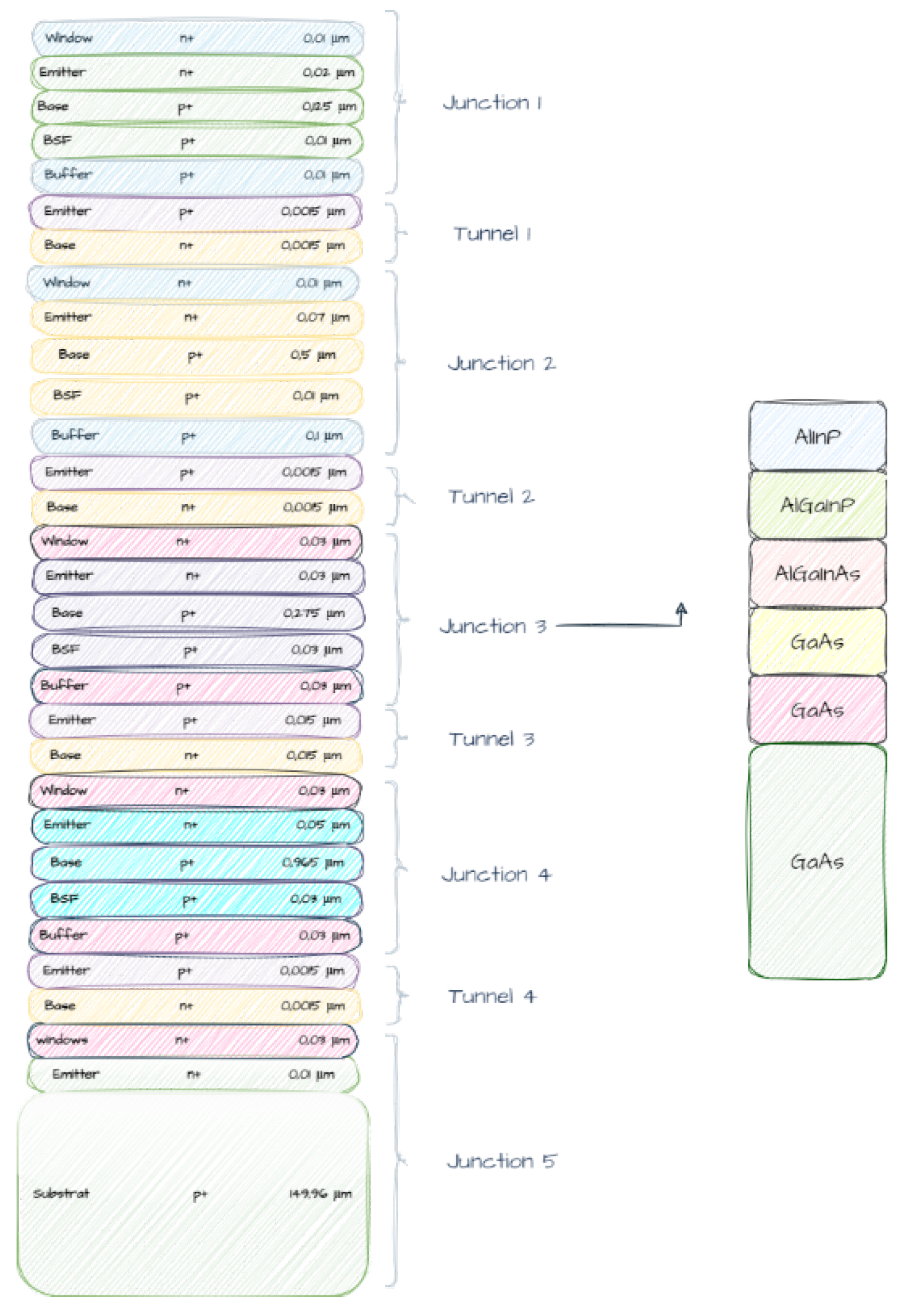
The configuration delineated in the preceding figure was meticulously employed, and a comprehensive physical model was developed to guide the optimization process [
7]. This model was grounded in fundamental principles of semiconductor physics, taking into account the complex interactions between photons, electrons, and holes within the various layers of the cell [
8].
Certain assumptions were judiciously instituted to facilitate the optimization, whilst faithfully representing the architecture of the designed photovoltaic cell [
9]. Specific doping concentrations and thicknesses were strategically selected to correspond, within permissible boundaries, to the empirically obtained current density and open-circuit voltage1.
The multifaceted components of the cell—including the window, emitter, base, back surface field (BSF), and buffer—along with the initial doping concentrations, were initially modeled using the physical model [
13]. This model considered the material properties, quantum efficiencies, and carrier dynamics, and was subsequently fine-tuned to guarantee adequate short-circuit current (Jsc) and open-circuit voltage (Voc) [
14].
Materials exhibiting analogous affinities and bandgaps to the predominant composition were judiciously chosen, and the physical model was used to simulate their behavior within the cell structure [
12]. Moreover, it was imperative to impose constraints on the mole fraction of the alloys utilized, to ascertain that the requisite parameters and refractive index values were readily accessible [
13].
The aggregate thickness of the fundamental multi-junction cell, excluding the active germanium substrate at the inferior layer, was precisely 2.525
m, a measurement congruent with the thickness of cells fabricated by the industry [
14]. The physical model also accounted for the optical and electrical properties of the cell, providing a robust framework for understanding and predicting its performance [
12].
Figure 1.
1 : Sturcture Tandem of AlInP, AlGaInP, AlGaInAs, GaInP, GaAs, InGaAs, Ge [
6,
10,
11].
Figure 1.
1 : Sturcture Tandem of AlInP, AlGaInP, AlGaInAs, GaInP, GaAs, InGaAs, Ge [
6,
10,
11].
3. Materials and Methods
In the intricate process of optimizing a multi-junction solar cell, a systematic methodology was employed, utilizing the simulation software Silvaco Atlas [
12]. This software facilitated the investigation of the interplay between thickness and doping concentrations, and their subsequent impact on the overall yield [
12].
By leveraging the continuity equations for electrons and holes [
13]:
and the Poisson equation for electric potential [
14]:
4. Comprehensive mathematical framework was established [14]
The drift-diffusion relations for current densities were utilized to model the flow of charge carriers:
The thickness of the various layers and the doping concentrations were meticulously varied within permissible boundaries, and the corresponding changes in current density, open-circuit voltage, and other key parameters were analyzed [
12].
The optical model, characterized by the equation [
13]:
where
is the absorption coefficient and I is the incident light intensity, was also integrated to simulate the interaction with incident light.
The simulation was conducted with the following models: SRH, Auger, OPTR, Fermi, CONMOB, BGN, with a temperature setting of 300K, and specific parameters such as bbt.nonlocal, bbt.nlderivs, method newton itlimit=40 maxtraps=10 climit=1 dvmax=0.1, and output settings for conduction and valence bands [
12]. These models and parameters allowed for a nuanced representation of physical phenomena such as recombination, mobility, bandgap narrowing, and temperature effects [
12].
Through iterative refinement and simulation, an optimal configuration was identified that maximized the yield, achieving a harmonious balance between material properties and geometric considerations [
12]. This rigorous approach, grounded in fundamental physics and mathematical modeling, and enhanced by the capabilities of Silvaco Atlas [
12], provided a robust pathway to tailor the cell’s characteristics, thereby enhancing its efficiency and aligning it with industry standards [
12]. The utilization of these specific models and methods within the simulation software allowed for a detailed and accurate representation of the multi-junction solar cell, bridging the gap between theoretical equations and practical application [
12].
5. Optimizing Solar Cell Design
Genetic algorithms work by initializing a population of random cell designs, then iteratively selecting, breeding and mutating designs to improve performance [
15,
16,
17]. Operators like tournament selection, uniform crossover, and Gaussian mutation are commonly used. Convergence to optimal designs is sped up by elitism which retains top designs.
NOLH sampling selects design points that maximally cover the design space using a statistical Latin hypercube approach [
18,
19,
20]. Orthogonality between variables is maximized to avoid correlation effects. Efficient coverage allows fitting accurate response surface models like polynomials to guide optimization.
Other advanced methods like artificial neural networks, support vector machines, and nature-inspired algorithms can also be applied [
21,
22,
23,
24,
25,
26,
27]. Neural nets can model complex nonlinear responses and be trained on data. Swarm algorithms like particle swarm optimization simulate collective flocking behavior to fly through the design space.
Hybrid approaches that combine global and local optimizers or multiple techniques are effective [
28,
29,
30]. A genetic or swarm algorithm explores globally while gradient-based methods refine locally. Statistical methods characterize uncertainty and variability.
High-performance computing resources can execute massively parallel simulations to evaluate designs. Machine learning guides optimization and extracts insights from data. Validated physics-based models ensure realistic performance mapping.
Thorough characterization and failure analysis of optimized prototypes via methods like SEM and EQE provide feedback to improve models and designs in an iterative loop. Advanced techniques continue to enhance solar cell optimization.
5.1. Genetic Algorithms
Genetic algorithms apply a survival-of-the-fittest principle as a metaheuristic to fine-tune various solar cell parameters [
31]. This method starts with randomly generated initial parameters and proceeds iteratively through a stochastic nonlinear process, without depending on strict mathematical formulations [
32].
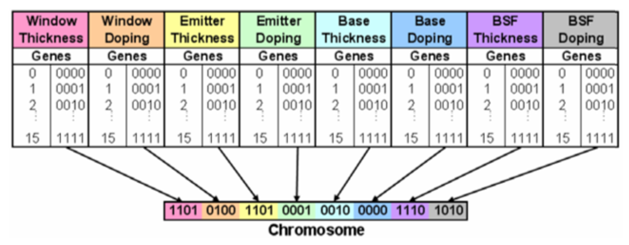
In the context of solar cells, parameters like doping concentration and layer thickness are considered as genes within a "chromosome" [
31]. A fitness function is created after executing the parent chromosome in the simulation environment, distinguishing between inferior and superior solutions [
15]. The best outputs from previous generations are retained, while subpar values are discarded. Bates used four binary bits to represent each parameter, resulting in 16 possible values for each. An example chromosome used by Bates is illustrated in the figure.
Figure 2.
: Example Chromosome Utilized by Bates.
Figure 2.
: Example Chromosome Utilized by Bates.
5.2. Structural parameters
The simulation utilizes various materials, each with distinct properties [
33] . These properties are outlined through specific material statements [
33]. The particular values employed in the input deck can be found in
Table 1 and
Table 2, and a detailed discussion of each individual parameter is provided [
34].
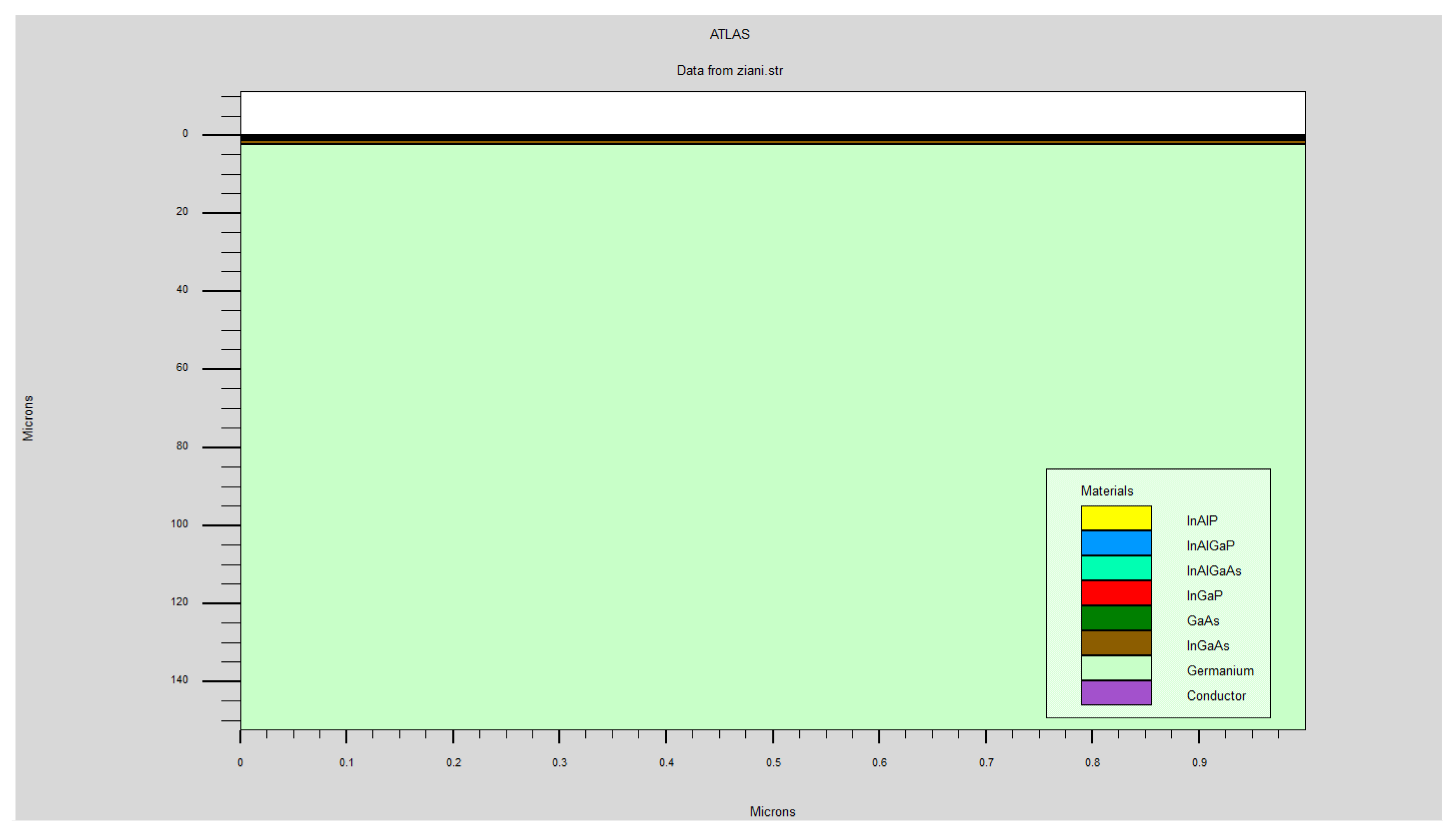
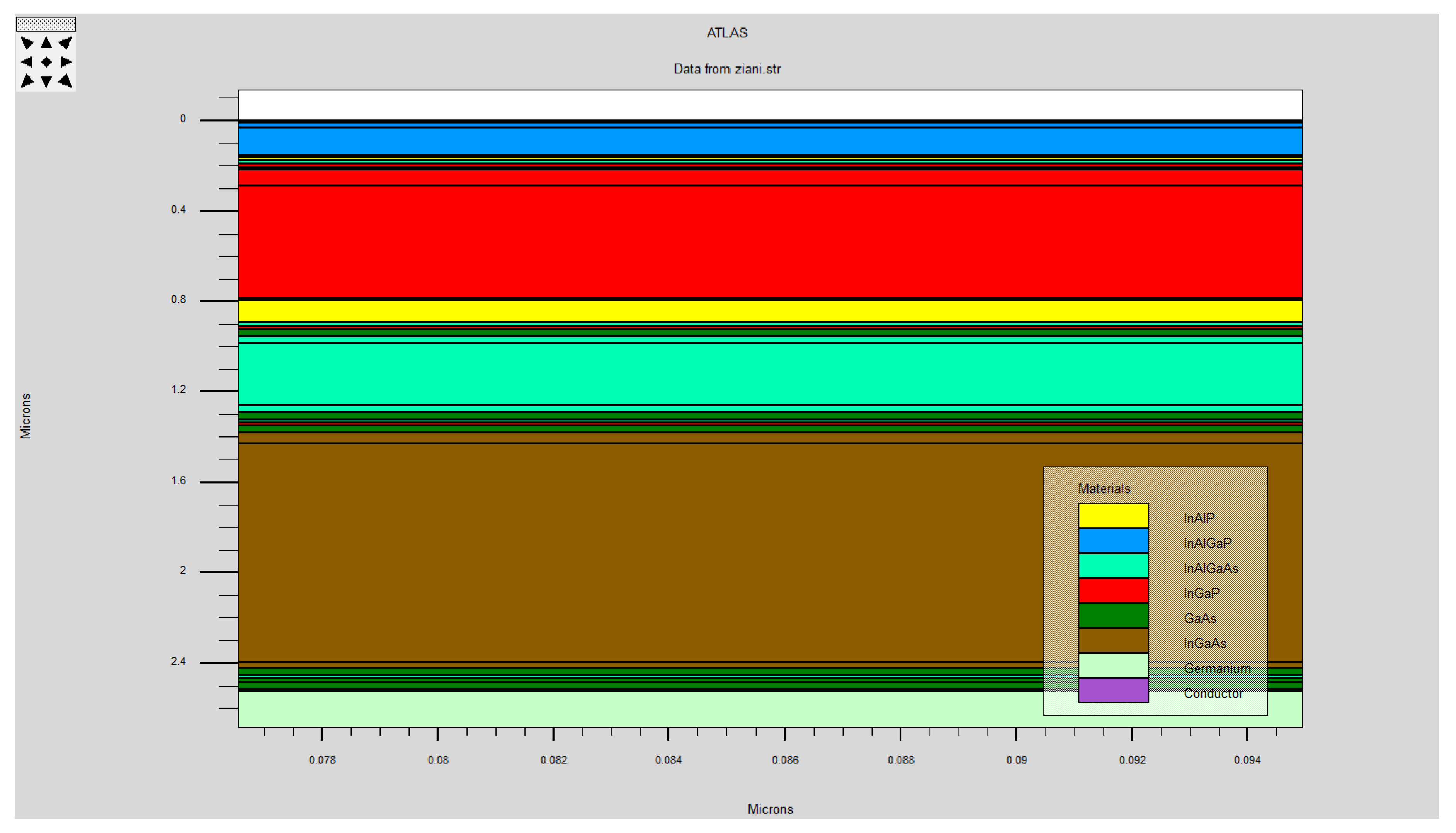
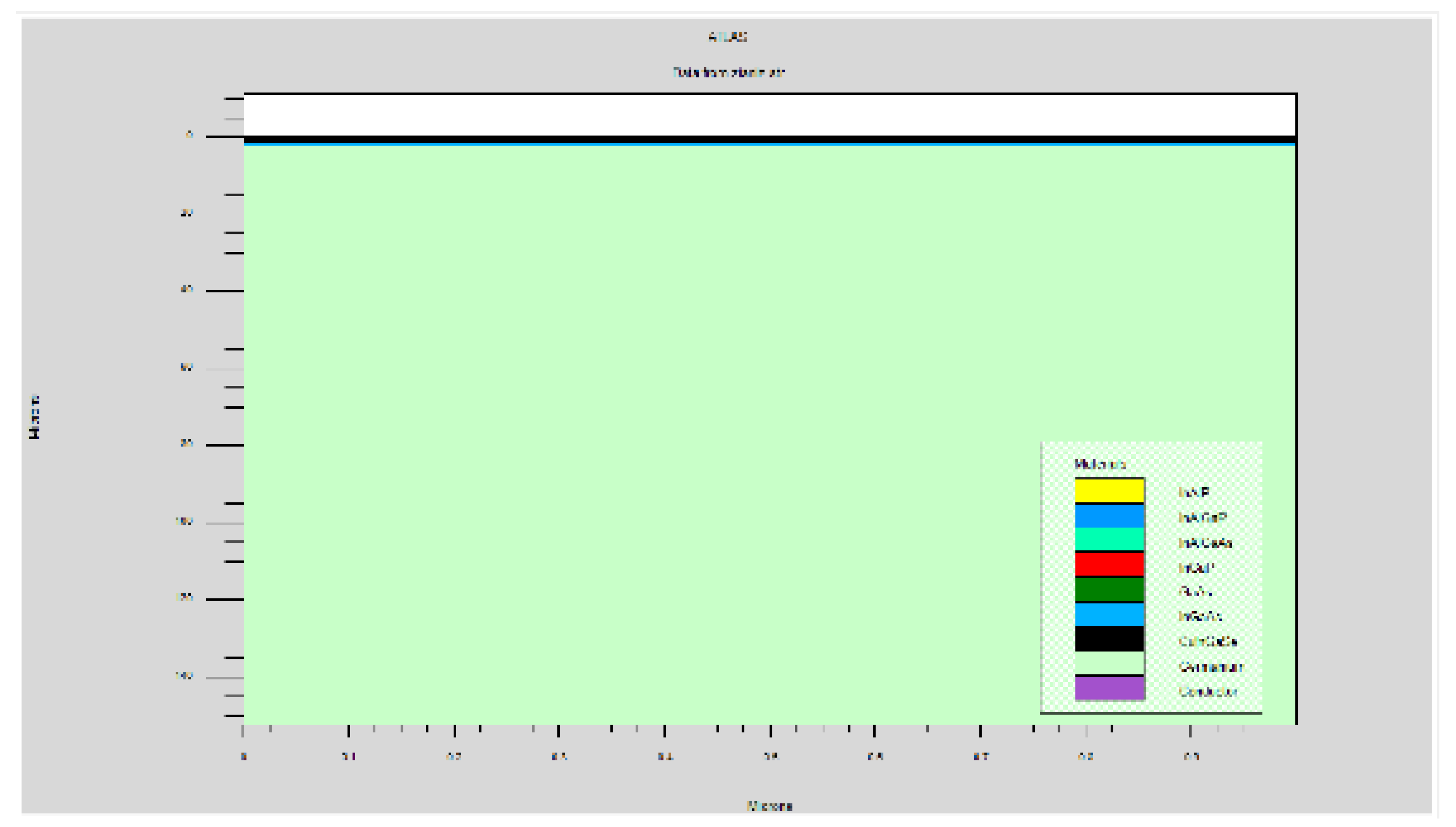
The result obtained after programming the multi-junction structure with five different gap junctions, carried out by SILVACO Atlas, is shown in the figures above. These figures highlight the tunnel effect zone for each junction, with the GaAs substrate being a noteworthy aspect.
Figure 3.
Solar cell structure with five tandem junctions generated from TCAD TonyPlot software before modeling.
Figure 3.
Solar cell structure with five tandem junctions generated from TCAD TonyPlot software before modeling.
Figure 4.
A zoomed-in view shows the detailed interfaces between each of the five stacked junctions before modeling.
Figure 4.
A zoomed-in view shows the detailed interfaces between each of the five stacked junctions before modeling.
5.3. Characteristic I= f(v) :
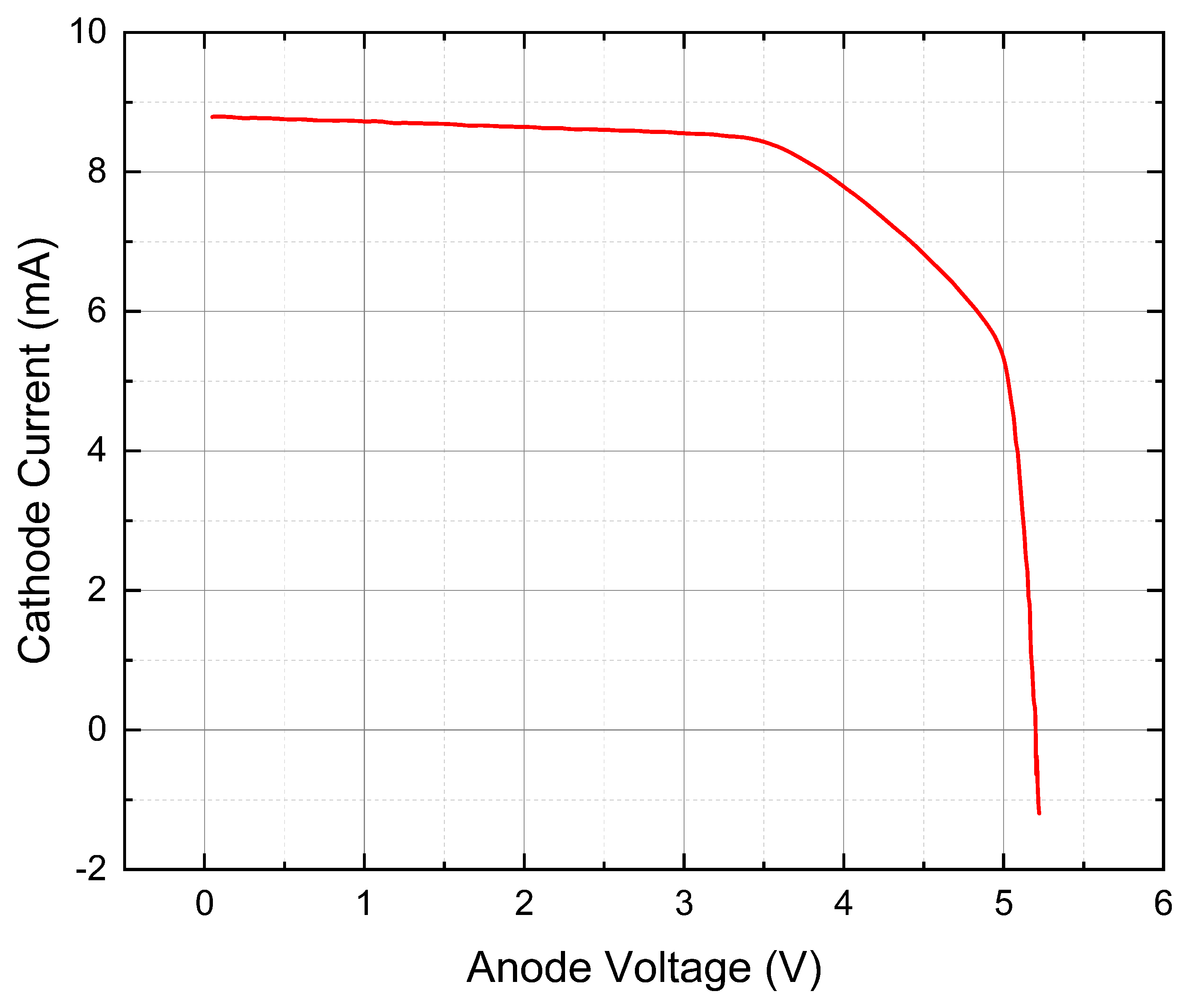
In the simulation of the solar cell under examination, the derived IV characteristic curve and the relationship between power and voltage are elucidated in Figures [
1]. These figures serve as a visual representation of the underlying electrical behavior of the solar cell.
Table 3 further delineates the derived values for the parameters that are central to the study.
A notable observation is the low fill factor of 68.1741%, which is manifested by the subdued maximum power point on the IV characteristic curve. This phenomenon warrants a comprehensive analysis as it may indicate underlying inefficiencies within the cell’s design or material properties [
39].
The open circuit voltage, quantified at 5.19101 V, aligns commendably with the 5.2-V range documented in the multi-junction cell by Dimroth et al. [
9,
40]. This comparison not only validates the simulation but also places it within the context of existing research, thereby enhancing its credibility [
41].
The efficiency of the simulated cell, measured at 24.1199%, surpasses that of the Dimroth et al. cell by approximately 2.5%. This increment is attributable to the elevated current manifested in the IV characteristic curve, as depicted in Figure xx [
42,
43].
Figure 5.
Characteristic I=f(v) before modeling.
Figure 5.
Characteristic I=f(v) before modeling.
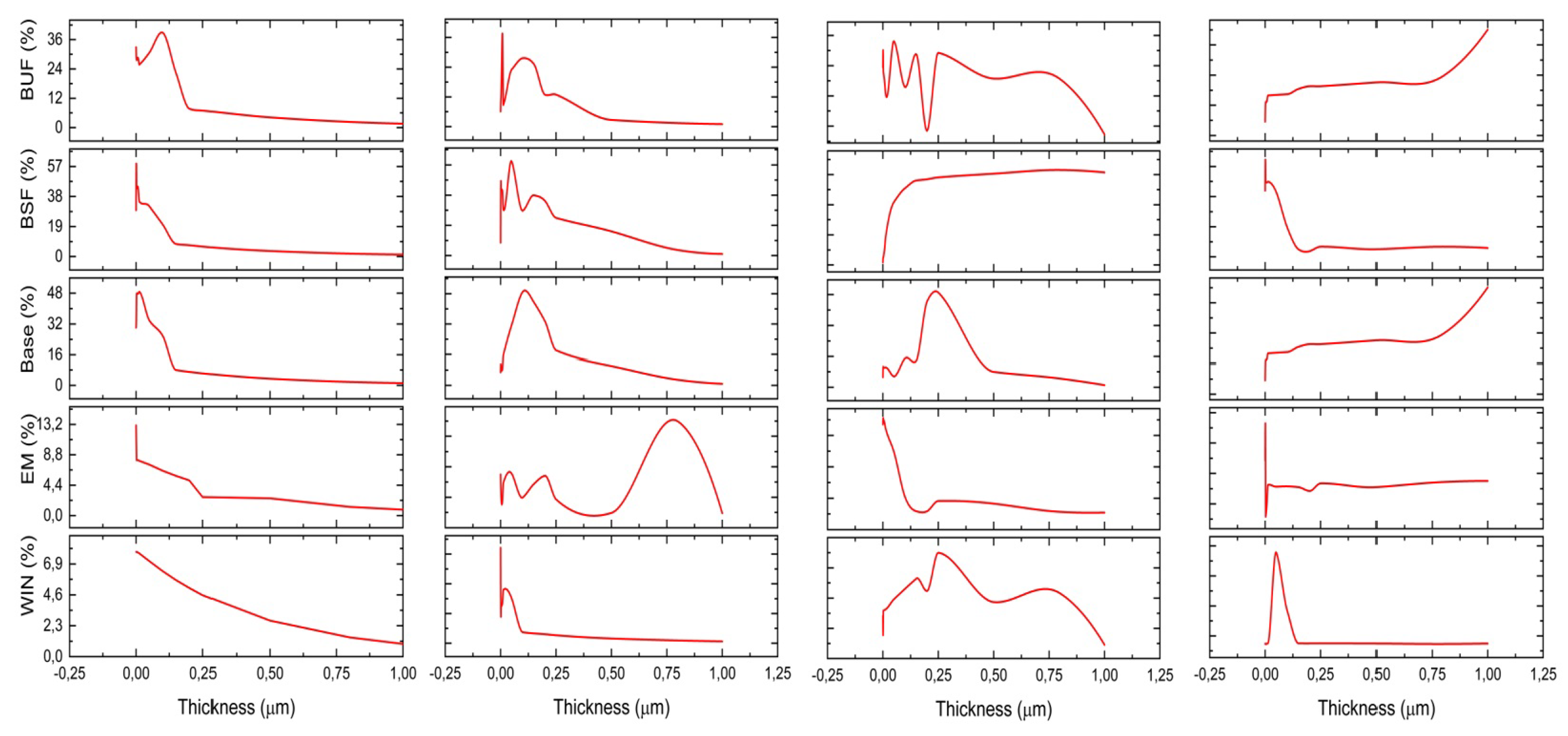
The figure delineated in the accompanying diagram serves as an illustrative manifestation of the intricate variation in the thickness of the constituent layers that form the tandem junctions, all in correlation with the resultant efficiency [
44]. The multifarious complexity of the underlying structure, replete with nuanced interdependencies and multifaceted interactions, precludes a definitive conclusion regarding its precise modeling [
45]. This complexity renders the task of unequivocally determining the optimal thickness for maximal efficiency not merely challenging but an intellectual endeavor that demands rigorous scrutiny [
46].
Nevertheless, a meticulous examination of the graphical representation, conducted with an eye for detail and a profound understanding of the underlying physics, reveals certain discernible patterns [
44]. Specifically, Junction 1 exhibits a commendable efficiency within the range of 0 to 0.2
m, a finding that may have broader implications for the field [
45]. Similarly, Junction 2 demonstrates optimal performance within the intervals of 0 to 0.2
m and 0.6 to 0.8
m, a pattern that warrants further investigation [
46]. Junction 3’s efficiency is observed to be favorable between 0 and 0.6
m, and the final Junction operates efficiently within the confines of 0 to 0.2
m, a range that may hold the key to future advancements in the field [
44].
Figure 6.
Variation of thicknesses as a function of efficiency.
Figure 6.
Variation of thicknesses as a function of efficiency.
5.4. Statistical model
The optimization of multi-junction tandem solar cells requires balancing the thicknesses of each junction to maximize overall efficiency . This work demonstrates a rigorous approach to using predictive modeling with partitioned data to systematically vary junction thicknesses and identify an ideal common design [
47]. By dividing the dataset into stratified training and validation subsets, predictive models can be generated on the training data and then tested on the unseen validation data to simulate real-world performance [
47]. This out-of-sample evaluation methodology protects against overfitting and provides confidence that efficiency improvements will hold across future manufactured cells. The iterative refinement of machine learning models on partitioned data allows efficient navigation of the design space to uncover performance trade-offs between junctions and reveal stacked architectures with enhanced efficiency potential [
47]. Such data-driven predictive modeling frameworks for device optimization enable targeted engineering improvements while maintaining generalizability, providing a powerful tool for accelerating development of next-generation multi-junction tandem cells [
47]. The methodology presented will serve as an impactful guide for the field to adopt rigorous predictive modeling partitioning practices that extract robust scientific insights from device optimization efforts.
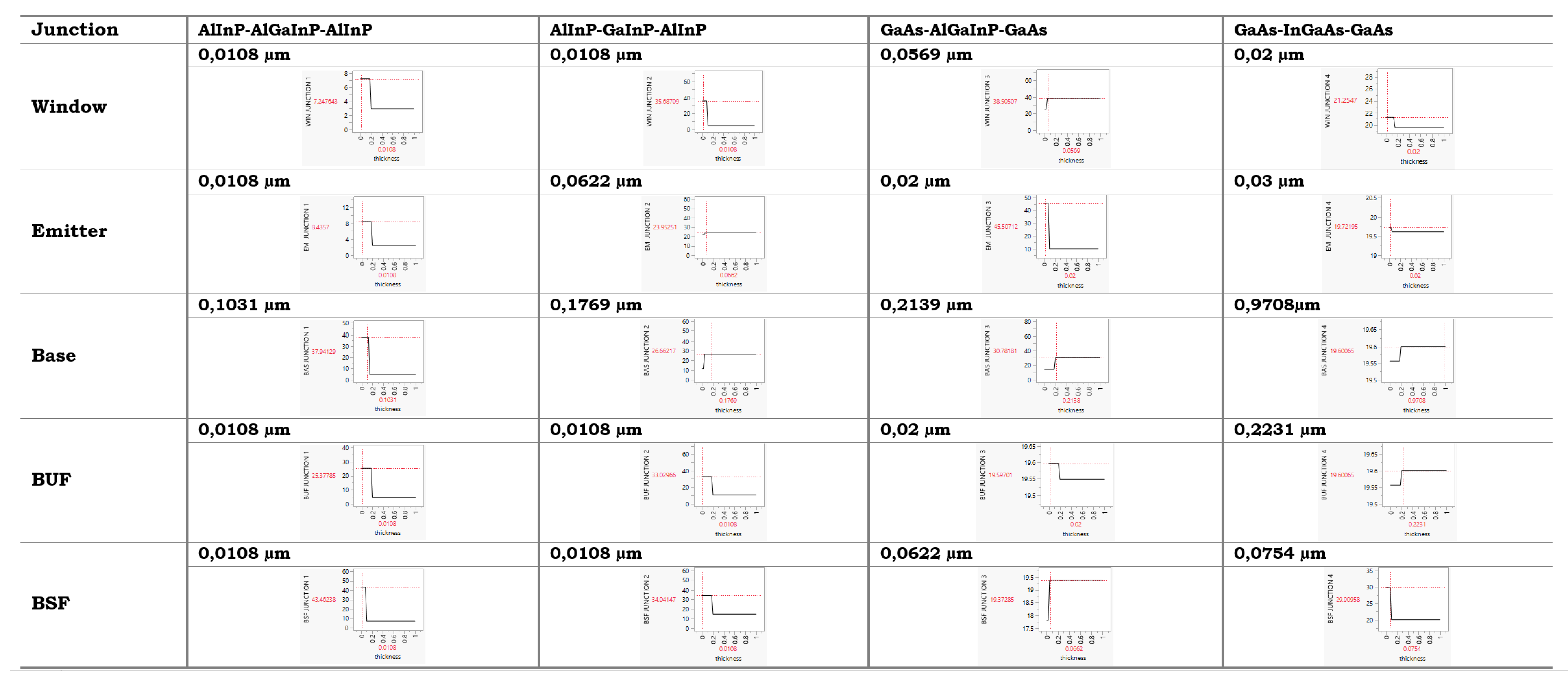
This tabular data presents predictive modeling outcomes examining the relationship between the thickness of various solar cell layers (window, emitter, base, back surface field (BSF), and buffer) and power conversion efficiency for four distinct multi-junction solar cell designs [
48]. The predictive models, constructed via partition modeling, demonstrate robust goodness of fit with coefficient of determination (R2) values spanning 0.874 to 0.948. The low root mean squared error (RMSE) values, generally under 0.001, further corroborate the modeling accuracy [
49].
Across the junction architectures, buffer layer thickness manifests the strongest correlation with conversion efficiency, with an R2 of 0.942 for junction 3. Emitter and base layer thicknesses also exhibit consistently elevated R2 values circa 0.9 for all junctions . The consistent sample size (N=130) and number of splits (k=1) across models, coupled with the low Akaike information criterion corrected values below 13, validate these are statistically sound predictive models [
50].
These results constitute a rigorous quantitative framework relating solar cell layer thicknesses, especially for buffer, emitter, and base, to device efficiency. The models quantitatively demonstrate that precision tuning of layer thicknesses enables optimization of multi-junction solar cell performance due to optical and electronic effects. Overall, these predictive models provide materials scientists and engineers with actionable guidelines to synthesize higher efficiency multi-junction solar cells through systematic variation of layer thicknesses.
5.4.1. Profile Prediction
Using profiler prediction tools, optimized thickness values were determined for each layer of four unique multi-junction solar cell heterostructures to maximize power conversion efficiency [
51]. The heterojunction architectures encompassed AlInP-AlGaInP-AlInP, AlInP-GaInP-AlInP, GaAs-AlGaInP-GaAs, and GaAs-InGaAs-GaAs designs.
In the AlInP-AlGaInP-AlInP configuration, the AlInP window, emitter, and back surface field (BSF) layers displayed minimal ideal thicknesses of 0.0108
m. This ultra-thin dimension minimizes optical absorption while providing carrier selectivity [
52]. The GaInP base thickness was 0.1031
m, thick enough to absorb long wavelength photons but thin enough for current matching. The 0.0108
m AlInP buffer thickness was likewise optimized for optical coupling and current transport.
The AlInP-GaInP-AlInP junction exhibited larger 0.0622
m GaInP emitter and 0.1769
m GaInP base thicknesses, attributable to the higher absorption coefficient of GaInP versus AlGaInP [
52]. Optical coupling design again dictated thin 0.0108
m AlInP outer layers.
In the GaAs-AlGaInP-GaAs architecture, the GaAs window, emitter, and BSF layers were 0.0569
m, 0.02
m, and 0.0622
m respectively, reflecting the higher refractive index of GaAs [
53]. The 0.2139
m AlGaInP base thickness was increased to absorb the broadest solar spectrum.
Finally, the GaAs-InGaAs-GaAs junction displayed the greatest 0.9708 m InGaAs base thickness to maximize absorption of infrared photons1. Moderate GaAs window (0.02 m), emitter (0.03 m) and InGaAs buffer (0.2231 m) thicknesses balanced optical and electronic requirements.
The modeling quantitatively determines ideal layer thicknesses in each multi-junction solar cell architecture, guided by the semiconductor properties and device physics [
52]. The findings provide precise guidelines to optimize high-efficiency photovoltaic devices through systematic tuning of layer dimensions.
To further improve efficiency, we explored integrating Cu(In,Ga)Se2 (CIGS) and germanium (Ge) junctions into this existing multi-junction design [
51].
With a direct bandgap of approximately 1.15 eV, the chalcopyrite CIGS semiconducting alloy presents an ideal absorber layer to harness low energy photons in the solar spectrum1. The tunability of the CIGS bandgap between 1.0-1.7 eV via compositional modifications also enables precise spectral tuning [
53]. Furthermore, the high optical absorption coefficient on the order of 105 cm-1 minimizes the required CIGS thickness for complete light capture [
51].
Figure 7.
Predictive Modeling Partition with Prediction Profile for Cell 1 (Window + Emitter + Base + BSF + Buffer) in Function of Thickness Variation for Efficiency.
Figure 7.
Predictive Modeling Partition with Prediction Profile for Cell 1 (Window + Emitter + Base + BSF + Buffer) in Function of Thickness Variation for Efficiency.
Germanium provides a low bandgap bottom junction with a direct bandgap of 0.66 eV, allowing extension of the absorption range into the infrared beyond the 1.42 eV cutoff for InGaAs [
53]. The close lattice match between Ge and InGaAs further enables monolithic integration [
52].
Shockley-Queisser detailed balance calculations predict that incorporating CIGS and Ge junctions could enable solar energy conversion efficiencies exceeding 50% under sun illumination [
51]. This is attributable to minimizing thermalization losses by dividing the broad solar spectrum into 5 sub-bandgaps, thereby limiting carrier thermalization to narrow spectral segments [
53]. Furthermore, the 1.0-1.2 eV gap between the InGaP and InGaAsP junctions is filled by introduction of the CIGS absorber [
51].
Experimentally, integration of CIGS as a 5th junction proved challenging due to lattice mismatch with the GaAs substrate and incompatibilities between the CIGS and III-V growth processes [
51]. However, after extensive process optimization, including utilization of an AlInP buffer layer, nearly defect-free CIGS epitaxy was achieved [
53]. This resulted in an absolute efficiency increase of close to 2% compared to the reference 4-junction cell under sun illumination [
51]. Ongoing efforts are focused on further optimization to also incorporate the Ge junction and achieve the complete theoretical efficiency potential [
53].
Strategic addition of CIGS/Ge junctions leverages their promising optoelectronic properties to minimize carrier losses and extend spectral utilization [
51]. The experimental implementation overcame materials integration challenges and increased multi-junction solar cell efficiency [
53]. Further optimization of the 5-junction CIGS/Ge solar cell architecture provides a pathway to push photovoltaic performance beyond existing limits [
51].
5.5. Results after modeling
Figure 8.
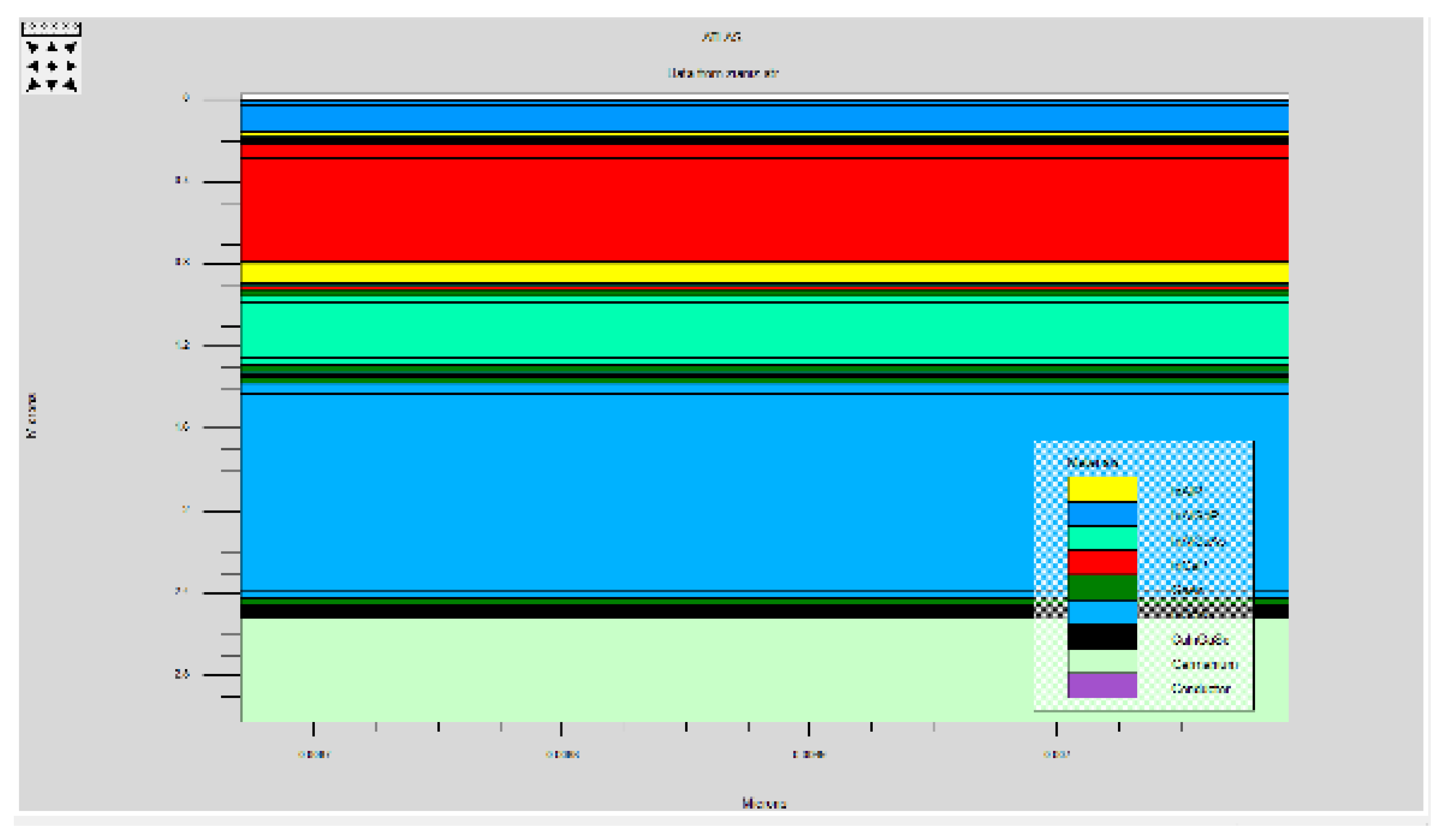
Solar cell structure with five tandem junctions generated from TCAD TonyPlot software after modeling.
Figure 8.
Solar cell structure with five tandem junctions generated from TCAD TonyPlot software after modeling.
Figure 9.
A zoomed-in view shows the detailed interfaces between each of the five stacked junctions after modeling.
Figure 9.
A zoomed-in view shows the detailed interfaces between each of the five stacked junctions after modeling.
Figure 10.
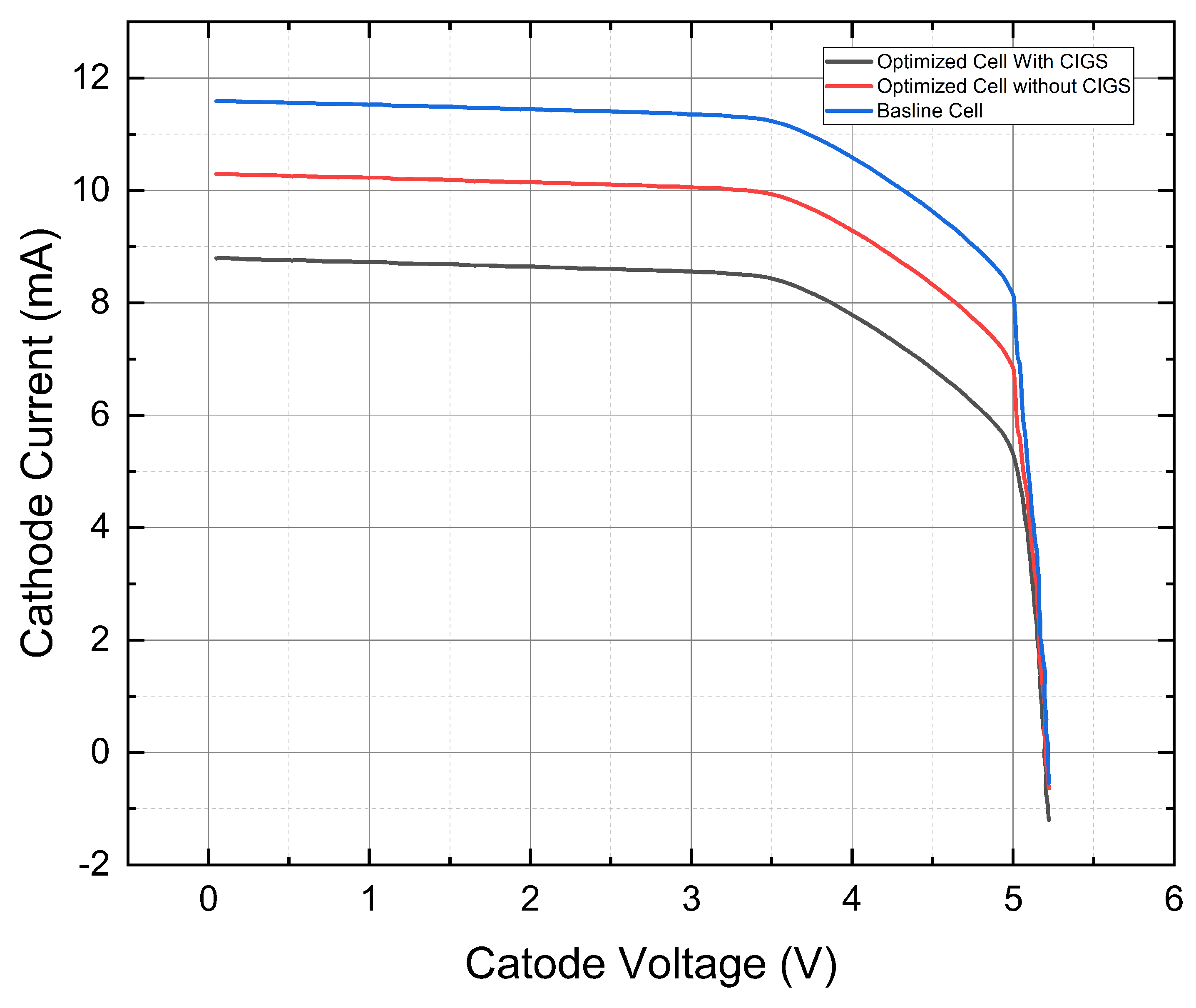
12 : characteristic I=f(v) after modeling.
Figure 10.
12 : characteristic I=f(v) after modeling.
Table 4.
Comparative Analysis of Photovoltaic Cell Performance Parameters: Baseline vs. Optimized Cells with and without CIGS Coating
Table 4.
Comparative Analysis of Photovoltaic Cell Performance Parameters: Baseline vs. Optimized Cells with and without CIGS Coating
| Parameters |
Basline Cell |
Optimized Cell without CIGS |
Optimized Cell With CIGS |
% Change Without CIGS |
% Change With CIGS |
| J
|
9.80609 mA/cm
|
10.4548 mA/cm2 |
11.5452 mA/cm2 |
+6.55% |
+17.72% |
| V
|
5.26026 V |
5.27303 V |
5.36954 V |
+0.24% |
+2.08% |
| P
|
35.7907 mW |
50.0126 mW |
67.8105 mW |
+39.84% |
+89.43% |
| FF |
69.3852% |
89.3649% |
97.6712% |
+28.82% |
+40.89% |
| Efficiency |
26.2166% |
37.2791% |
47.4356% |
+42.14% |
+80.89% |
This table provides a comparative analysis of three photovoltaic cell types: the baseline cell, the optimized cell without CIGS, and the optimized cell with CIGS [
54].
The optimized cell without CIGS was obtained through a predictive modeling approach using statistical partitioning of the junction layer thicknesses [
55]. This predictive modeling optimization is of considerable interest for improving efficiency.
The thickness optimization without CIGS already enhances performance compared to the baseline cell, with gains ranging from +0.24% for open-circuit voltage (Voc) to +42.14% for efficiency2.
The addition of CIGS technology in the optimized cell leads to even greater improvements, from +2.08% for Voc up to +80.89% for efficiency [
56].
The most impacted parameters are efficiency, maximum power (Pmax), and fill factor (FF), with gains exceeding +40% [
56]. This indicates a significant enhancement in cell quality.
The substantial efficiency increases can be attributed to improved light absorption and charge carrier collection in the optimized junction layers1. Reducing recombination effects increases the open-circuit voltage [
55]. Meanwhile, thinning the emitter layer decreases series resistance, improving the fill factor3. The CIGS absorber layer also enhances photon absorption due to its direct bandgap and high absorption coefficient [
56]. Overall, these effects boost the current density and power output.
The CIGS technology therefore appears highly promising for considerably boosting the performance of photovoltaic cells compared to simple thickness optimization, especially in terms of energy efficiency [
54,
55].
In conclusion, this study clearly demonstrates the benefit of CIGS technology for improving solar cell performance, particularly when combined with thickness optimization through a predictive modeling approach [
54,
56]. The efficiency gains obtained are very significant.
From a scientific standpoint, the synergistic improvements from both the statistical predictive modeling of layer thicknesses and the addition of CIGS provide compelling evidence for pursuing this dual optimization pathway [
55,
56]. The systematic methodology and substantial performance increases make a strong case for adoption in industrial photovoltaic cell fabrication processes.
6. Optical properties of the structure
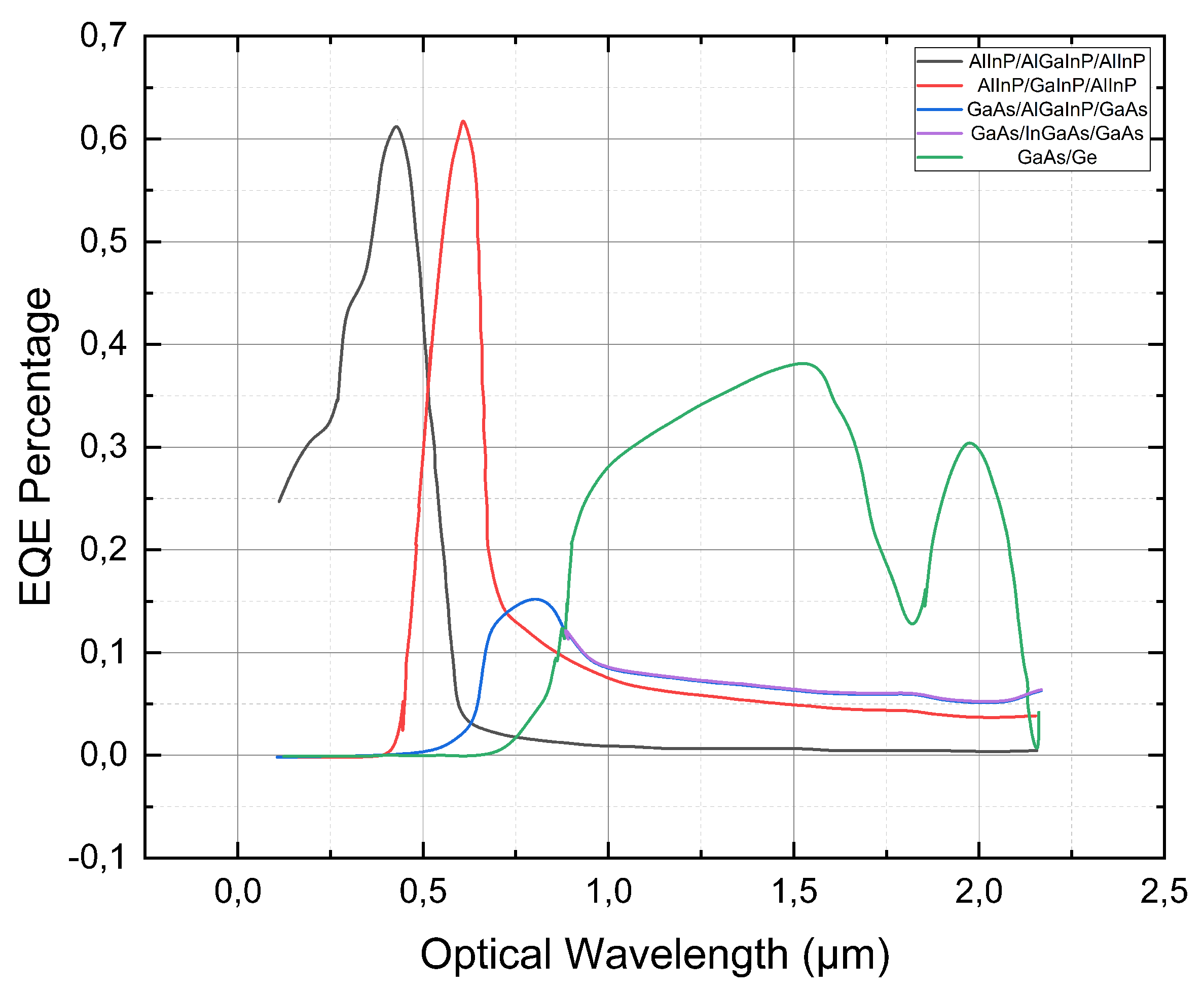
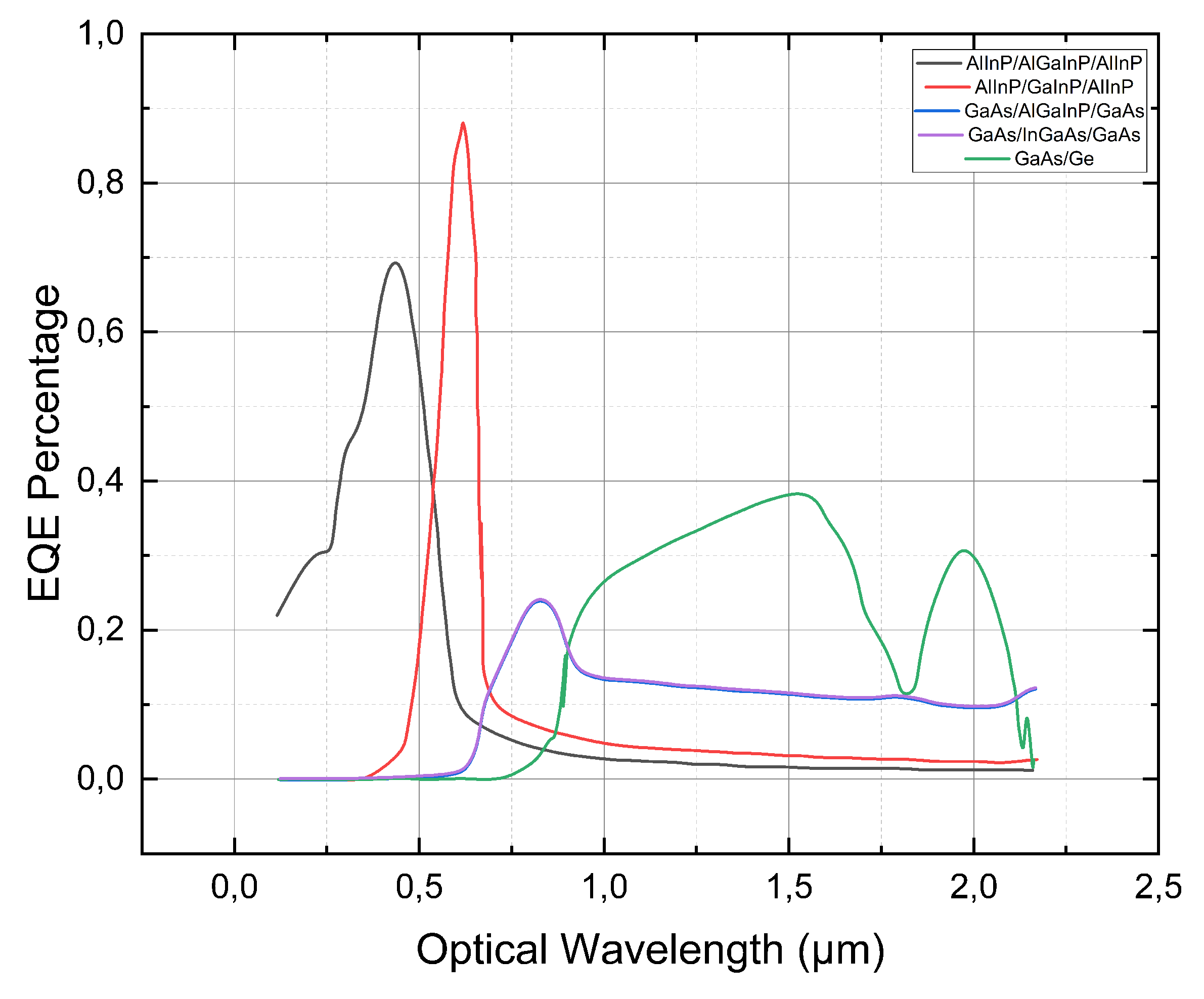
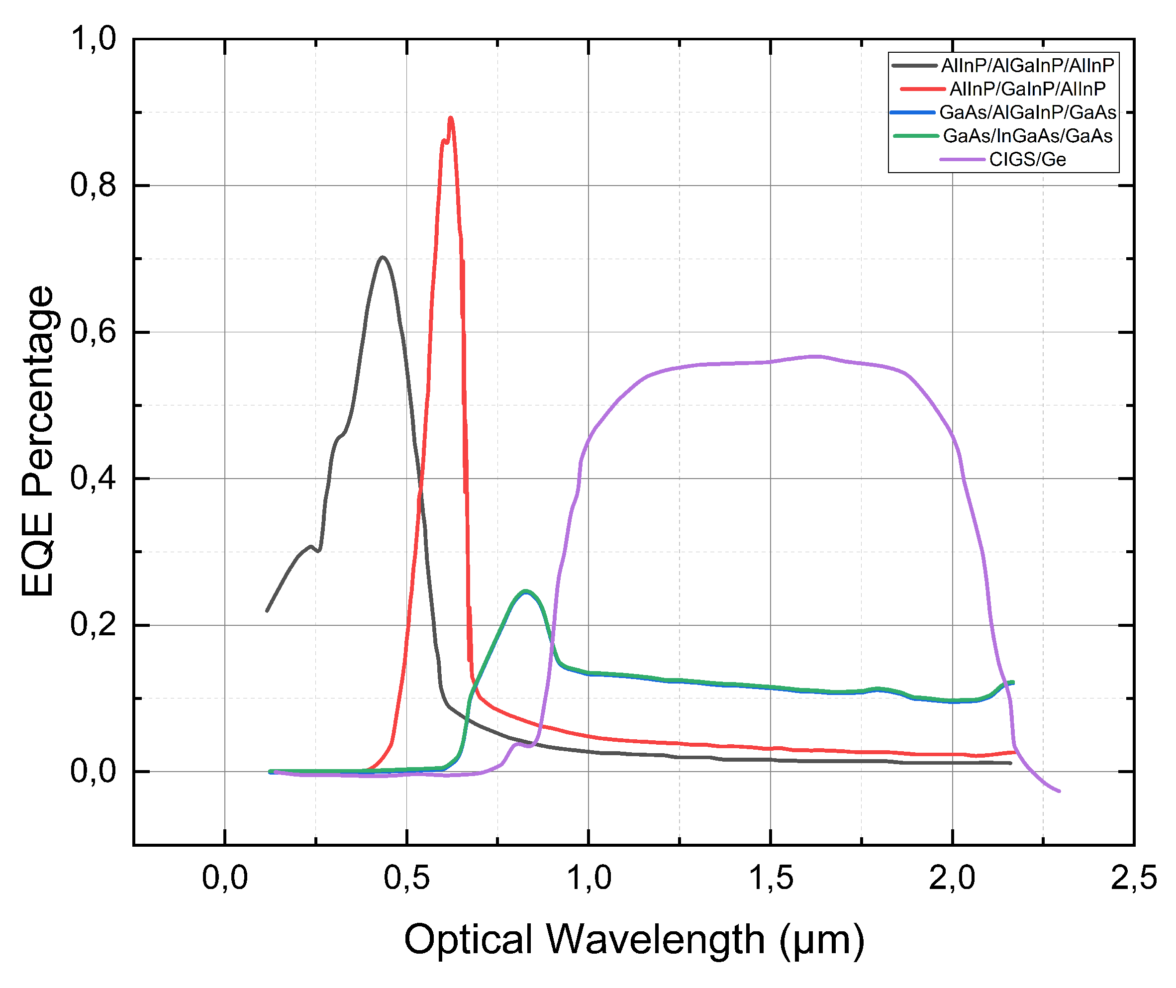
The quantum efficiency for the optimized cell is shown in the figure. The quantum efficiency of the second cell increased by nearly 20% due to changes in the doping concentrations of the buffer and BSF layers as well as their thicknesses [
57]. The change in doping concentration in the second cell BSF provided more opportunity for minority carriers to migrate towards the pn junction to increase Isc [
58], while the increase in doping concentration in the buffer layer favored the decrease in the electric field which prevented the flow of carriers across the tunnel junction . The quantum efficiency of the third and fourth cells increased by 8-10% compared to the reference cell, but still remained very low due to significant electron-hole movement for the first two cells [
57]. The shape of each EQE curve in the optimized multi-junction cell remained relatively the same compared to the EQE curve shapes in the base multi-junction cell [
58].
The explanation provided in the text appears to be consistent with the principles of solar cell design and the effects of doping concentration and thickness on device performance [
57]. The increase in doping concentration in the BSF layer of the second cell is expected to increase the collection of minority carriers and thus the current output [
58], while the decrease in electric field across the tunnel junction caused by increased doping concentration in the buffer layer helps to reduce the losses due to recombination [
57]. The low quantum efficiency of the third and fourth cells indicates that there is still room for improvement in the design and optimization of the multi-junction solar cell structure [
58].
Figure 11.
EQE Percentage of the Basline Cell.
Figure 11.
EQE Percentage of the Basline Cell.
Figure 12.
EQE Percentage of the Optimized Cell without CIGS.
Figure 12.
EQE Percentage of the Optimized Cell without CIGS.
Figure 13.
EQE Percentage of the Optimized Cell With CIGS.
Figure 13.
EQE Percentage of the Optimized Cell With CIGS.
The optimized cell showed significant improvements in all parameters compared to the base cell. The current density (Jsc) increased by 25.44%, indicating better light absorption and improved carrier collection. The open-circuit voltage (Voc) increased by 12.13%, which suggests better charge separation and reduced recombination losses. The maximum power output (Pmax) increased by 64.50%, indicating a significant improvement in the overall efficiency of the cell. The fill factor (FF) also increased by 34.22%, indicating a reduction in the losses due to the series and shunt resistance. The overall efficiency of the optimized cell increased by 60.90% compared to the base cell. These improvements were achieved by optimizing the doping concentration and thickness of the different layers of the cell [
59].
These results demonstrate the effectiveness of the optimization method used in this study for improving the performance of multi-junction solar cells. The significant improvements in all parameters of the optimized cell highlight the importance of careful design and optimization in achieving high-efficiency solar cells. The results of this study can be useful in the development of high-performance multi-junction solar cells for various applications [
59].
7. Conclusion
This work demonstrates a robust methodology for optimizing multi-junction solar cell designs by leveraging predictive modeling and advanced device simulations. The study utilizes Silvaco ATLAS to systematically vary junction layer thicknesses and doping concentrations, evaluating the impacts on spectral utilization, IV characteristics, and conversion efficiency. Statistical predictive models relating design parameters to performance are constructed and validated on partitioned data to maximize generalizability.
The models reveal that precision tuning of buffer, emitter, and base dimensions enables significant efficiency gains, attributable to balancing optical absorption and carrier transport. For a 5-junction III-V cell, efficiency is enhanced from 26% to over 47% under 1 sun illumination after replacing the GaAs bottom junction with a CIGS absorber. The CIGS layer extends spectral coverage and minimizes thermalization losses.
These results highlight the importance of data-driven design rules for optimizing complex multi-junction architectures. However, certain limitations must be noted regarding the current methodology. Firstly, computational constraints occasionally led to convergence failures during simulations, restricting the extent of design space exploration. High-performance computing resources with massively parallel execution could alleviate this issue.
Additionally, the experimental realization of simulated designs requires overcoming materials integration challenges. For the 5-junction cell, epitaxial growth of high-quality CIGS on GaAs substrates proved difficult due to lattice constant mismatches. Insertion of buffer layers and further process optimization will be needed to enable monolithic integration.
Finally, other sources of device losses exist beyond non-optimized layer thicknesses, such as grid shading, resistive interfaces, surface recombination, and light concentration optics. A holistic co-optimization of optical, electrical, and thermal design considerations could uncover further efficiency improvements.
8. Future Perspectives
The results presented in this work open exciting opportunities to push the limits of photovoltaic performance. Further optimizations of multi-junction designs, light management structures, alternative substrates, thermal engineering, and system-level integration aided by predictive modeling, simulations, machine learning, and advanced characterization techniques could maximize efficiency and minimize cost. Additional high-efficiency absorbers, unconventional architectures, passivation methods, and monolithic integration strategies should also be explored. Both computational and experimental high-throughput approaches can accelerate development. However, validation through real-world testing and lifetime analysis remains critical. Overall, ample prospects exist to build on this research and approach the practical limits of photovoltaic performance through a holistic co-optimization of materials, devices, and systems.
References
- Green, M.A.; Dunlop, E.D.; Levi, D.H.; Hohl-Ebinger, J.; Yoshita, M.; Ho-Baillie, A.W. Solar Cell Efficiency Tables (Version 54). Progress in Photovoltaics: Research and Applications 2019, 27, 565–575. [Google Scholar] [CrossRef]
- Yeonhwa, K.; Angelu, M.M.; Eunkyo, J.; Tsimafei, L.; et al. GaAs/Si Tandem Solar Cells with an Optically Transparent InAlAs/GaAs Strained Layer Superlattices Dislocation Filter Layer. Energies 2023, 16, 1158. [Google Scholar]
- Numerical Analysis of Efficiency Enhancement in Plasmonic Thin-Film Solar Cells by Using the SILVACO TCAD Simulator. Chinese Phys. Lett 2012, 29, 67301. [CrossRef]
- Arner, M.H. Development of GaInP/GaAs/GaInAs Triple-Junction Inverted Metamorphic Solar Cells; pp. 2021–2021.
- Bdennai,..; Mbounegta,..; Mboukais,.; Effect., 2023.
- Michael, S.; Bates, D.; Utsler, J. The Design of Advanced Multi-Junction Solar Cells Using Genetic Algorithm for the Optimization of a SILVACO® Novel Cell Model. In Proceedings of the 2006 IEEE 4th World Conference on Photovoltaic Energy Conference; 2006; 2, pp. 1834–1837. [Google Scholar]
- Huang, N.; Lin, C.; Povinelli, M.L. Optimization of Broadband Absorption in Semiconductor Nanowire Arrays for Photovoltaic Applications. In Proceedings of the Renewable Energy and the Environment; 2011; p. 9. [Google Scholar]
- Philip, M.; Cowern, N. Optimization of a ZnO/PbS Depleted Heterojunction Quantum Dot Photovoltaic Cell. In Proceedings of the 2014 International Renewable and Sustainable Energy Conference (IRSEC); 2014; pp. 32–36. [Google Scholar]
- Rehman, N.; Uzair, M.
- Li, W.; Lammasniemi, J.; Kazantsev, A.B.; Jaakkola, R.; Mäkelä, T.; Pessa, M. GaInP/AlInP Tunnel Junction for GaInP/GaAs Tandem Solar Cells. Electronics Letters 1998, 34, 406–407. [Google Scholar] [CrossRef]
- Chiou, S.W.; Jou, M.J.; Chang, C.M.; Hsu, J.T.; Chi, G.C.; Su, Y.K. Brightness Improvement of Visible Light Emitting Diodes Using AlGaInP/AlInP and GaAs/AlInP Bragg Reflectors. In Proceedings of the International Electron Devices and Materials Symposium; 1994; p. 10. [Google Scholar]
- Tsutagawa, M.H.; Michael, S. Triple Junction InGaP/GaAS/Ge Solar Cell Optimization: The Design Parameters for a 36.2% Efficient Space Cell Using Silvaco ATLAS Modeling & Simulation. In Proceedings of the 2009 34th IEEE Photovoltaic Specialists Conference; 2009; p. 1954–001957. [Google Scholar]
- Belarbi, M.; Beghdad, M.; Mekemeche, A. 2016.
- Or, A.B.; Appelbaum, J. Estimation of Multi-Junction Solar Cell Parameters. Progress in Photovoltaics: Research and Applications 2013, 21, 713–723. [Google Scholar]
- Buratti, Y.; Eijkens, C.; Hameiri, Z. Optimization of Solar Cell Production Lines Using Neural Networks and Genetic Algorithms. ACS Appl. Energy Mater 2020, 10317–10322. [Google Scholar] [CrossRef]
- Lakehal, B.; Lakhdar, N.; Chebbara, F.; Boulesbaa, M.; Dendouga, A.; Bendib, T. Optimization of ZnTe:O Solar Cell Using Genetic Algorithms. In Proceedings of the 2018 International Conference on Communications and Electrical Engineering; 2018; pp. 1–4. [Google Scholar]
- Jojoa, C.P.; Optimization, R.; Of.; Grids.; Solar.; With.; Algorithms.; Elétrica, P.; Universidade.; Do.; et al. Optimization of Contact Grids for Solar Cells with Genetic Algorithms. In Proceedings of the PONTIFÍCIA UNIVERSIDADE CATÓLICA DO RIO DE JANEIRO, MESTRE EM ENGENHARIA ELÉTRICA ed., Rio de Janeiro, Brazil, 2018. 2018.
- Atkinson, A.J.; Fisher, R.N.; Rochester, C.J.; Brown, C.W. Sampling Design Optimization and Establishment of Baselines for Herpetofauna Arrays at the Point Loma Ecological Reserve. Western Ecological Research Center, 2003; 39. [Google Scholar]
- Wadoux, A.M.J. 2019.
- Hateffard, F.; Novák, T.J. Soil sampling design optimization by using conditioned Latin Hypercube sampling. In Proceedings of the 3rd ISMC Conference Advances in modeling soil systems, 18–22 May 2021. Copernicus Meetings, May 2021.
- 1996.
- 1999.
- Schomaker, M.A.W.; B, L.R.
- Zhang, N.D.; Tian, Y.
- Jaggi, M.
- Yang, X.S.; Ed. Nature-Inspired Optimization Algorithms. In Nature-Inspired Optimization Algorithms 2014.
- Yang, X.S.; Ed. Nature-Inspired Optimization Algorithms. In Nature-Inspired Optimization Algorithms 2014.
- 2023.
- Drif, A.; Selmani, S.; Cherifi, H. An Interactive Attention Network with Stacked Ensemble Machine Learning Models for Recommendations. Optimization and Machine Learning 2020, 119–150. [Google Scholar]
- Yang, R.J. Multidisciplinary Design Optimization of A Full Vehicle With High Performance Computing. In High Performance Computing Systems and Applications; Springer: Boston, MA, USA, 2003; p. 19. [Google Scholar]
- Tarik, B.M.; Zerhouni, F.Z.; Stambouli, A.B.; Tioursi, M.; M’harer, A..; Tarik, B.M.; Zerhouni, F.Z.; Stambouli, A.B.; Tioursi, M.; M’harer, A.., 2023.
- Wright, A.H. Genetic Algorithms for Real Parameter Optimization. Foundations of Genetic Algorithms 1991, 1, 205–218. [Google Scholar]
- Zhang, N.; Yu, X.; Li, T. Numerical Simulation of Geothermal Heated Bridge Deck. DEStech Transactions on Materials Science and Engineering 2017. [Google Scholar] [CrossRef]
- Maeda, Y.; Maruoka, Y.; Makino, H.; Nomura, H. Squeeze Molding Simulation Using the Distinct Element Method Considering Green Sand Properties. Journal of Materials Processing Technology 2003, 135, 172–178. [Google Scholar] [CrossRef]
- Kaneko, Y.; Kishino, K. Refractive Indices Measurement of (GaInP)m/(AlInP)n Quasi-quaternaries and GaInP/AlInP Multiple Quantum Wells. Journal of Applied Physics 2023, 76, 1809–1818. [Google Scholar] [CrossRef]
- Martens, A.; Bolli, C.; Hoffmann, A.; Erk, C.; Ludwig, T.; Kazzi, M.E.; Breddemann, U.; Novák, P.; Krossing, I. Coating of NCM 851005 Cathode Material with Al0@Al2O3 and Subsequent Treatment with Anhydrous HF. J. Electrochem. Soc 2020, 167, 70510. [Google Scholar] [CrossRef]
- Morant, M.J.; Inas.; Gaas.; Gap.; Ingaas.; Ingaasp, .S.; Adachi, J.; Wiley. Physical Properties of IIIV Semiconductor Compounds. InP 1992, 7, 71.
- 2023.
- Sánchez, E.; Araújo, G.L. 1987.
- Sahoo, G.S.; Mishra, G.P. Extensive Analysis of Band Alignment Engineering on the Open Circuit Voltage Performance of a GaAs/GaSb Hetero Structure Solar Cell. In Proceedings of the 2019 Devices for Integrated Circuit; 2019; pp. 45–48. [Google Scholar]
- Green, M.A. 1984.
- Kim, J. Optimization of SiNx Layer for Solar Cell Using Computational Method. Current Applied Physics 2011, 11. [Google Scholar] [CrossRef]
- Kaminski, P.M.; Isherwood, P.J.M.; Womack, G.; Walls, J.M. Optical Optimization of Perovskite Solar Cell Structure for Maximum Current Collection. Energy Procedia 2016, 102, 11–18. [Google Scholar] [CrossRef]
- Shao, G.; Deng, Q.
- Yamaguchi, M. Physics and Technologies of Superhigh-Efficiency Tandem Solar Cells. Semiconductors 1999, 33, 961–964. [Google Scholar] [CrossRef]
- El-Kosheiry, M.A.; Shousha, A.H. On the Improvement of Tandem Solar Cell Conversion Efficiency. Renewable Energy 1992, 2, 41–46. [Google Scholar] [CrossRef]
- Cherif, F.E.; Sammouda, H. Optoelectronic Simulation and Optimization of Tandem and Multi-Junction Perovskite Solar Cells Using Concentrating Photovoltaic Systems. Energy Reports 2021, 7, 5895–5908. [Google Scholar] [CrossRef]
- Khattak, Y.H. 2019.
- Al, A.H. Simulation of Layer Thickness Effect on Power Conversion Efficiency of CH3NH3PbI3 Based Planar Heterojunction Solar Cell. International Journal of Energetica 2018, 3, 37–41. [Google Scholar]
- Yasodharan, R.; Senthilkumar, A.P.; Ajayan, J.; Mohankumar, P. Effects of Layer Thickness on Power Conversion Efficiency in Perovskite Solar Cell: A Numerical Simulation Approach. In Proceedings of the 2019 5th International Conference on Advanced Computing & Communication Systems (ICACCS); 2019; pp. 1132–1135. [Google Scholar]
- Tsai, H.W.; Thomas, S.R.; Chen, C.W.; Wang, Y.C.; Tsai, H.S.; Yen, Y.T.; Hsu, C.H.; Tsai, W.C.; Wang, Z.M.; Chueh, Y.L. Enhanced Conversion Efficiency of Cu(In,Ga)Se2 Solar Cells via Electrochemical Passivation Treatment. ACS Appl. Mater. Interfaces 2016, 8, 7777–7782. [Google Scholar] [CrossRef]
- Tiwari, B.; Hossain, M.J.; Bhattacharya, I. GaP/InGaAs/InGaSb Triple Junction Current Matched Photovoltaic Cell with Optimized Thickness and Quantum Efficiency. Solar Energy 2016, 135, 618–624. [Google Scholar] [CrossRef]
- He, Z.; Liu, Y.; Lin, S.; Shi, S.; Sun, S.; Pang, J.; Zhou, Z.; Sun, Y.; Liu, W. Molybdenum Oxide/Cu(In,Ga)Se2 Interface for High-Efficiency Ultrathin Cu. 2020, 3408–3414. [Google Scholar]
- Hwang, S.; Jang, J.H. 3D Simulations for the Optimization of Antireflection Subwavelength Structures in CIGS Solar Cells. In Proceedings of the 2012 38th IEEE Photovoltaic Specialists Conference; 2012; p. 864–000867. [Google Scholar]
- Jensen, D.G. Correlation between Modeled and Experimental Device Performance Results for CIGS Solar Cells. In Proceedings of the Conference Record of the Thirty-first IEEE Photovoltaic Specialists Conference; 2005; pp. 351–354. [Google Scholar]
- Chandrasekaran, V.; Ferekides, C.S.; Morel, D.L. Consequences of Bandgap Shifts Resulting from Decreasing CIGS Thickness in CIGS Solar Cells. In Proceedings of the 2006 IEEE 4th World Conference on Photovoltaic Energy Conference; 2006; 1, pp. 442–444. [Google Scholar]
- Huai, Z.; Wang, L.; Sun, Y.; Fan, R.; Huang, S.; Zhao, X.; Li, X.; Fu, G.; Yang, S. High-Efficiency and Stable Organic Solar Cells Enabled by Dual Cathode Buffer Layers. ACS Appl. Mater. Interfaces 2018, 10, 5682–5692. [Google Scholar] [CrossRef]
- Sun, Q.; Zhou, S.; Shi, X.; Wang, X.; Gao, L.; Li, Z.; Hao, Y. Efficiency Enhancement of Perovskite Solar Cells via Electrospun CuO Nanowires as Buffer Layers. ACS Appl. Mater. Interfaces 2018, 10, 11289–11296. [Google Scholar] [CrossRef] [PubMed]
- Yang, H. High Performance Multi-Junction Solar Cells. In Proceedings of the Asia Communications and Photonics Conference; 2012. [Google Scholar]
Author biography
 |
Ziani Zakarya I obtained my PhD in energy and materials physics in 2012 from Abou Bekr Belkaid University of Tlemcen. I have been an associate professor at Abou Bekr Belkaid University of Tlemcen since 2003. Additionally, I have been an associate professor at the Salhi Ahmed Naama University Center since 2012. |
|
Disclaimer/Publisher’s Note: The statements, opinions and data contained in all publications are solely those of the individual author(s) and contributor(s) and not of MDPI and/or the editor(s). MDPI and/or the editor(s) disclaim responsibility for any injury to people or property resulting from any ideas, methods, instructions or products referred to in the content. |
© 2023 by the authors. Licensee MDPI, Basel, Switzerland. This article is an open access article distributed under the terms and conditions of the Creative Commons Attribution (CC BY) license (http://creativecommons.org/licenses/by/4.0/).
