1. Introduction
As an ideal detector for photons with weak optical power, superconducting nanowire single photon detectors (SNSPDs) have numerous emerging applications, including but not limited to quantum key distribution [
1,
2], deep space communication [
3], single photon lidar systems [
4], and mass spectrometry [
5]. Since the first SNSPD demonstrated in 2001, which exhibited low system detection efficiency (SDE) [
6], researchers have made substantial strides in overcoming limited SDE by employing different optical cavity designs. Highly efficient SNSPDs have been developed primarily through the use of metallic [
7,
8] or dielectric mirrors [
9,
10]. These developments contributed to the realization of SNSPDs with near-unity detection efficiencies at certain target wavelengths. Nevertheless, many reported detectors are still limited in terms of bandwidth, exhibiting high SDE across a bandwidth typically a few hundred nanometers around a singlet resonant wavelength, preventing SNSPDs from fully exploiting the potential of broader wavelength ranges. To extend the detection bandwidth, recent efforts in developing broadband or multispectral SPSNDs take advantage of multiple optical absorption resonances [
11,
12] or multilayer-nanowire structures [
13,
14,
15], thus extending the detection bandwidth, providing solutions for a wider range of applications, such as fluorescence correlation spectroscopy [
16], singlet oxygen luminescence detection [
17], as well as ranging and imaging [
18,
19].
Despite many recent efforts to create broadband or multispectral SNSPDs, current designs exhibit limited photon wavelength sensitivity because the voltage pulse pattern of the detector is insensitive to variations of incident single photon wavelength. To address the limited photon wavelength sensitivity problem in existing multispectral or broadband SNSPD designs, we present a dual-spectral SNSPD that can detect incident single photons at two well-separated detection bands with high NbN nanowire absorbance. By stacking a distributed Bragg reflector (DBR) designed to target wavelengths between 1070 and 1400 nm on a gold mirror and placing all four layers of NbN nanowires at positions exhibiting strong absorption resonance, a dual-spectral SNSPD is realized. As opposed to previous multispectral SNSPD designs, the detector presented in this work can categorize absorbed photons into either of the two detection bands based on their wavelength, making the SNSPD design proposed in this work a potential solution for interesting applications for future quantum communication technology, which might require one to distinguish different signals based on varying photon wavelength.
2. SNSPD Design and Materials
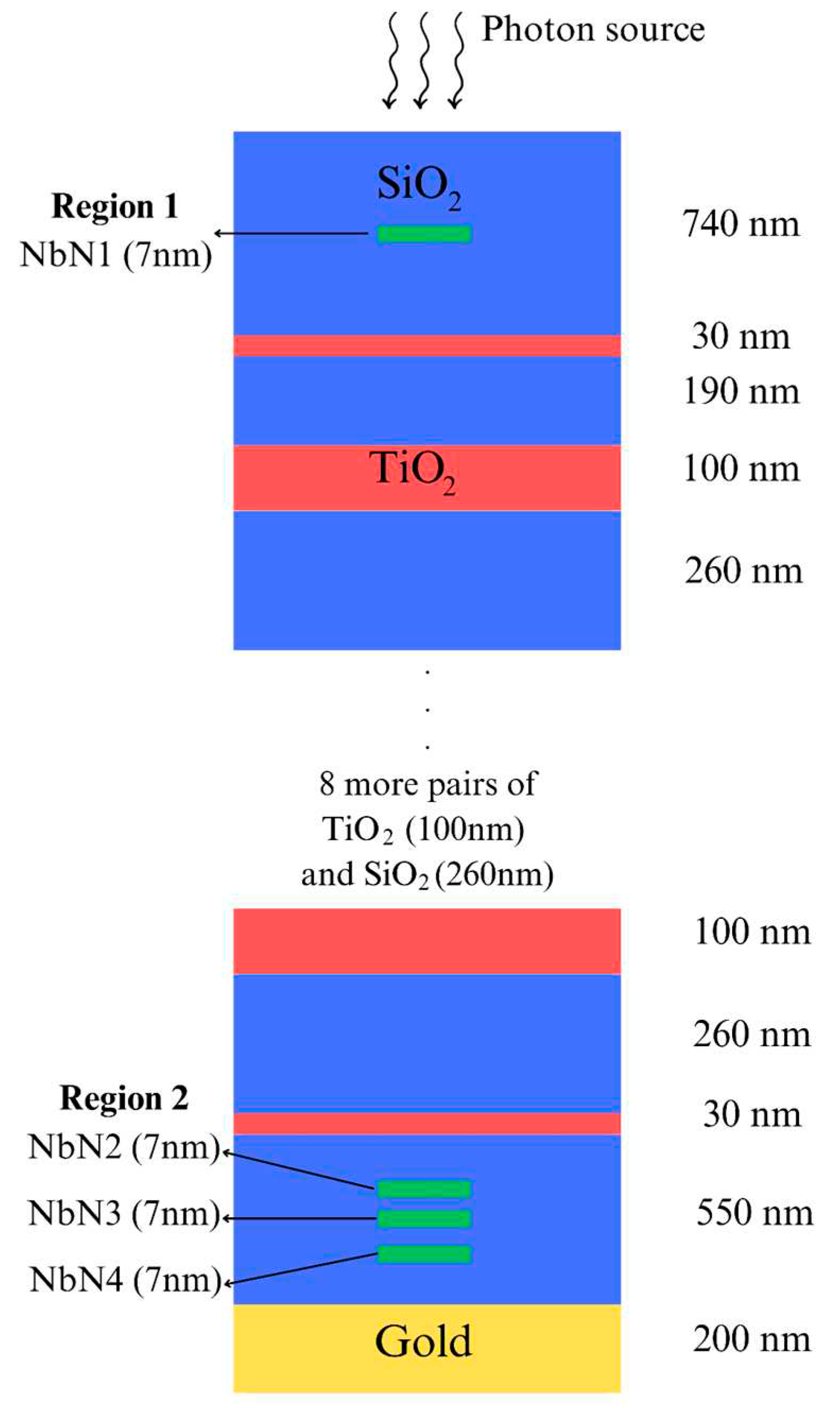
The SNSPD design is depicted in figure 1. The structure presented contains an alternating SiO2/TiO2 DBR on top of a 200 nm gold mirror as the cavity. The proposed design also utilizes a total of 4 layers of nanowires, for single photon detection. As shown in figure 1, there is one layer of nanowire placed in Region 1 (upper region) and three layers of nanowires stacked in Region 2 (lower region). Each nanowire has a thickness of 7 nm, and all layers, including the dielectric and the gold mirror, are tuned to maximize absorption resonance at the position where the nanowires are placed.
Figure 1.
Schematic of the simulated structure. Nanowires are 7nm thick and have SiO2 spacers in between one another. In the simulation, the photon source is normally incident onto the structure as shown.
Figure 1.
Schematic of the simulated structure. Nanowires are 7nm thick and have SiO2 spacers in between one another. In the simulation, the photon source is normally incident onto the structure as shown.
Ideally, the nanowire in Region 1 is sensitive to photons with wavelengths of about 1143 nm while the three layers of nanowires positioned in Region 2 are sensitive to photons with wavelengths within the range of 1440 to 2000 nm.
3. Simulation and Results
The following section outlines the simulation results. To calculate the reflectance of the dielectric stack above the gold mirror, the transfer matrix method was employed. As for electric field intensity and nanowire absorbance calculations, the Ansys Lumerical finite-difference time-domain (FDTD) solver was utilized.
3.1. Band selection DBR
The DBR employed in the proposed SNSPD differs from conventional ones, where each layer's thickness is typically set as
, with
being the target wavelength and
representing the real part of the refractive index of the dielectric material employed. Through the utilization of a modified DBR design, where the layers with higher refractive index possess a thickness less than
, and layers with lower refractive index have a thickness greater than
, together with appropriate adjustments in the thickness of dielectrics within the three initial and final layers, it becomes possible to mitigate the adverse effects of higher-order interference as well as high-order modes of constructive interference that causes unwanted spectral ripples in conventional DBR [
20,
21]. Since the DBR serves both as a mirror and a filter, reflecting photons within the 1070 to 1400 wavelength range while allowing photons with wavelengths > 1400 to pass through, high-order modes of constructive interference must be mitigated to ensure high transmittance in the desired wavelength range. The reflectance-wavelength graphs of a conventional DBR targeting 1230 nm and a modified DBR, with a structure shown in figure 2a, are depicted in figure 2b.
Figure 2.
(a) Schematic of the simulated modified DBR. In this design, the gold mirror, some of the SiO2 above the gold mirror, and all layers of the proposed SNSPD’s nanowires are removed; (b) The reflectance as a function of wavelength for conventional and modified DBR.
Figure 2.
(a) Schematic of the simulated modified DBR. In this design, the gold mirror, some of the SiO2 above the gold mirror, and all layers of the proposed SNSPD’s nanowires are removed; (b) The reflectance as a function of wavelength for conventional and modified DBR.
As shown by figure 2b, the modification does not heavily influence the reflectance in the region near the target wavelength. While the modified DBR’s ability to eliminate higher order interference is compromised with the addition of thick SiO2 layers and the gold mirror below it, the modified DBR still proves to work better than conventional DBR designs.
With the DBR acting as a mirror and a filter that primarily reflects light with wavelengths ranging from 1070 to 1400 nm, it is possible to create two well separated absorption bands through the addition of a gold mirror and three layers of NbN nanowires below the DBR. Since gold has high reflectance in the infrared region, it reflects most of the photons passing through the dielectric stack.
3.2. Dual-band mirror using modified DBR + Gold
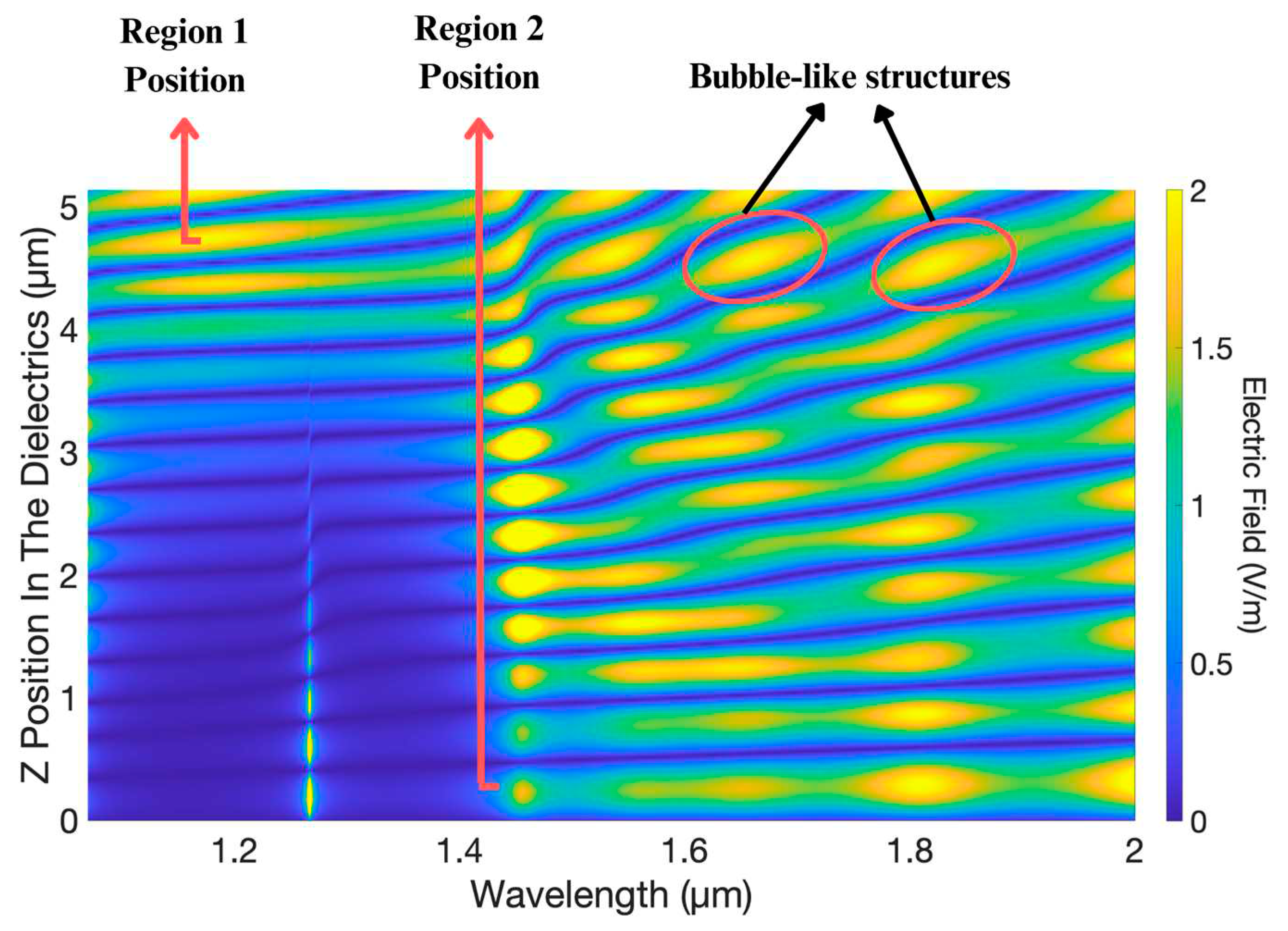
In order to identify the optimum position to place the nanowires, the electric field intensity within the dielectrics is calculated, as shown in figure 3. The electric field colormap demonstrates the principle concept behind a dual-spectral SNSPD. Thanks to the DBR above the gold mirror, most photons with wavelengths ranging from 1070 to 1400 nm are reflected in the first few layers of the dielectric stack.
Figure 3.
FDTD simulated electric field intensity profiled by the wavelength and the Z position in the dielectric layers above the gold mirror of the SNSPD. The NbN nanowires are then positioned at places with the strongest electric field intensity. In this colormap, it is obvious that the first few layers of the dielectric stack filtered out most photons with wavelengths from 1070 to 1400 nm before they reached the layers below.
The reason for the electric field intensity variation that creates bubble-like structures in the colormap is due to the interference introduced by thicker layers of SiO2, such as the layers with thicknesses of 550 nm and 740 nm. At times, the interference pattern introduced by these layers might lead to low nanowire absorption at certain wavelengths. Thus, thicker dielectrics in the SNSPD should be carefully tuned and optimized to a specific desired thickness, maximizing the absorption resonance at the region where the nanowires are placed.
Another point to note in the electric field intensity colormap shown in figure 3 is that photons with wavelengths > 1400 nm still have considerable electric field strength in multiple layers of the dielectric stack due to the gold mirror’s high reflectance. This effect is one of the limitations of this device. Due to the strong electric field in the uppermost SiO2 layer, when a NbN nanowire is inserted in Region 1, it will also absorb some photons with longer wavelengths. To mitigate this effect, three layers of nanowires are stacked in the SiO2 layer between the gold mirror and the DBR.
3.3. Dual-spectral SNSPD
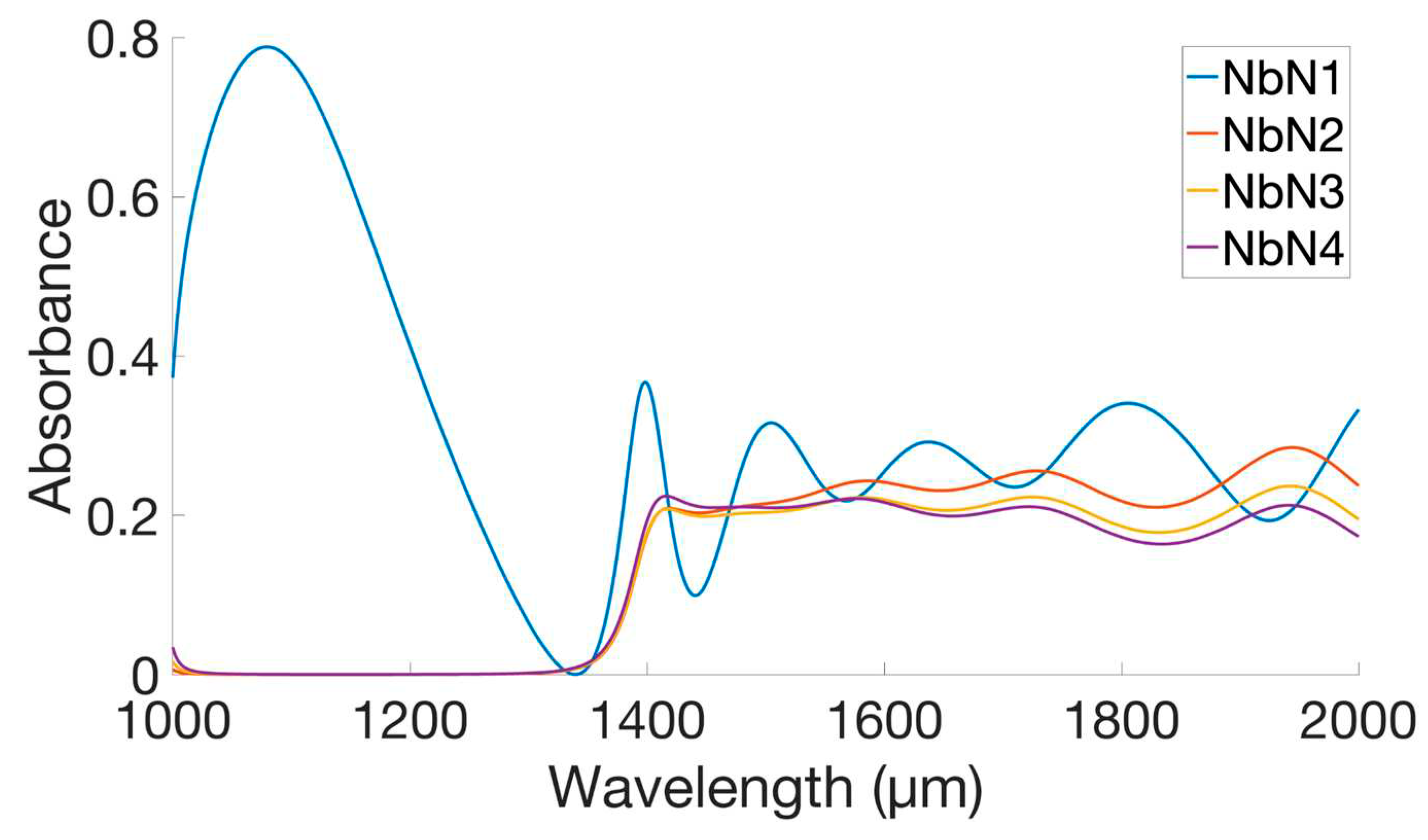
After inserting 4 layers of NbN nanowires with a thickness of 7 nm into the structure according to the design shown in figure 1, figure 4 illustrates the absorbance of each nanowire.
Note: as shown in figure 1, Region 1 (upper region) consists of NbN1, and Region 2 (lower region) contains NbN2, NbN3, and NbN4.
Figure 4.
The absorbance of each nanowire is shown. The absorbance of NbN1, or the uppermost nanowire in the SNSPD design, peaks at 1143 nm with a value of 0.788. As for NbN2, the nanowire demonstrates an absorbance > 0.2 for wavelengths from 1450 to 2000 nm. For NbN3, its absorbance is > 0.178 for wavelengths from 1440 to 2000 nm. Finally, NbN4 exhibits an absorbance > 0.163 for wavelengths ranging from 1435 nm to 2000 nm.
Figure 4 highlights the effect of the DBR, which blocks most photons with wavelengths 1070~1400 nm from reaching nanowires positioned in Region 2. Also, while the DBR employed in this design has high reflectance from 1070 to 1400 nm, since it remains challenging to control the phase dispersion and interference introduced by the dielectric stack [
13], the absorption band in the shorter wavelength region is very limited. On the contrary, a gold mirror has not only good reflectance in the infrared region but also ignorable phase dispersion, enabling a relatively constant absorbance for wavelengths from 1440 nm onwards.
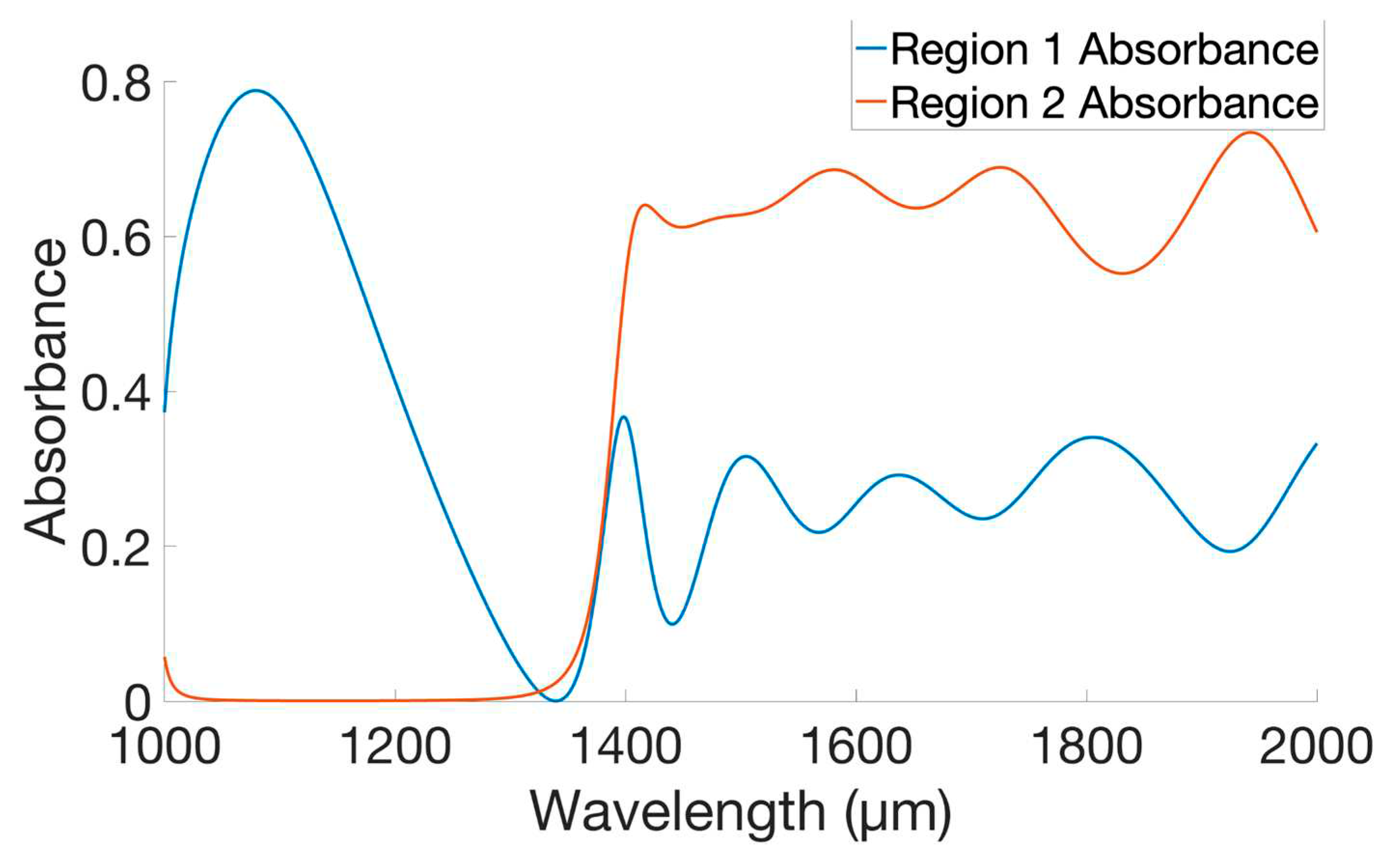
Figure 5 shows the total absorbance of nanowires placed in Region 1 and Region 2.
Figure 5.
The absorbance of nanowires in Regions 1 and 2 is shown. Region 1 exhibits a peak absorbance at 1143 nm, reaching a value of 0.788, and Region 2 has a total absorbance > 0.55 for all wavelengths ranging from 1440 to 2000. The total absorbance of all 4 layers of nanowires combined demonstrates high SDE.
From figure 5, the dual-spectral characteristic of the SNSPD can be readily observed. The nanowire in Region 1 primarily absorbs photons with wavelengths around 1143 nm and the nanowires in Region 2 (NbN2–NbN4) are responsible for absorbing photons with wavelengths from 1440 to 2000 nm.
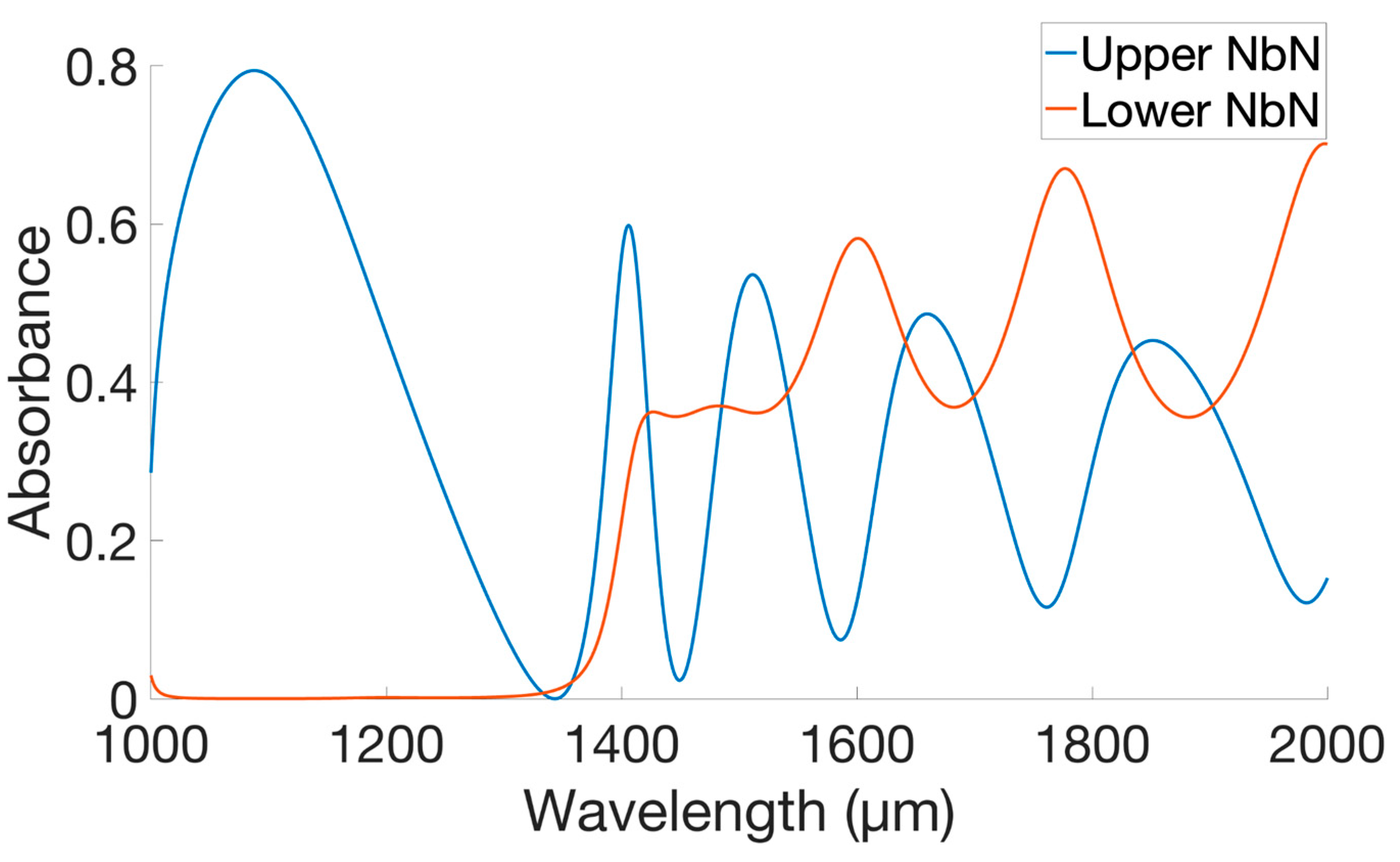
To demonstrate the effect of multilayer nanowires, figure 6 depicts the simulated absorbance when just two NbN nanowires are utilized. Compared to the original dual-spectral SNSPD, this new design removes two nanowires in Region 2, leaving the detector with a nanowire in the uppermost SiO2 layer and another between the modified DBR and the gold mirror.
Figure 6 shows the simulated absorbance of these two nanowires.
Figure 6.
Simulated absorbance of the upper and lower nanowires in a SNSPD structure reduced to just two nanowires. The peak absorbance of the upper nanowire has a value of 0.794 at the wavelength 1151 nm. The lower-positioned nanowire has an absorbance > 0.355 for wavelengths 1460 to 2000 nm.
Figure 6.
Simulated absorbance of the upper and lower nanowires in a SNSPD structure reduced to just two nanowires. The peak absorbance of the upper nanowire has a value of 0.794 at the wavelength 1151 nm. The lower-positioned nanowire has an absorbance > 0.355 for wavelengths 1460 to 2000 nm.
After comparing the two absorbance-wavelength graphs in figure 6 to those in figure 5, it is evident that the addition of more nanowires in Region 2 successfully decreases the uppermost nanowire’s high absorbance at certain wavelengths > 1400 nm, creating a more desirable dual-spectral SNSPD with the capability to distinguish between photons with wavelengths in distinct absorption bands.
4. Discussion
Unlike previous efforts in creating multispectral or broadband SNSPDs, the dual-spectral SNSPD proposed in this work utilizes both multilayer-nanowire structures and multiple optical absorption resonances.
Rather than placing multiple layers of nanowire on top of the structure as demonstrated in the work of Li et al. [
13] or employing a thickness-modulated optical film stack that generates multiple absorption resonances on the dielectric mirror surface as demonstrated by the work of Wang et al. [
12], inserting nanowires in between a DBR and a gold mirror enables each nanowire to focus on absorbing photons with certain wavelengths, enabling the realization of a dual-spectral SNSPD capable of distinguishing incident single photons based on whether they have a wavelength of about 1143 nm or within the 1440 to 2000 nm region.
Here, we also demonstrate why multiple layers of nanowires are utilized. Due to the high reflectance of the gold mirror and strong electric field intensity in the first SiO2 layer, the uppermost NbN has high absorption potential for some wavelengths > 1400 nm. To better achieve an ideal dual-spectral SNSPD with this design, multiple layers of NbN nanowires are employed to mitigate this unwanted effect. According to the simulation results, this approach proves to be effective as we observe a significant drop in absorbance for the nanowire positioned in Region 1 for longer wavelengths.
Nevertheless, this device still has two limitations. The first arises from the phase dispersion caused by the DBR, resulting in a significantly constrained bandwidth for wavelengths around 1143 nm. Second, due to absorption resonance introduced by the gold mirror in the first few layers of the DBR, the uppermost nanowire embedded within the first SiO2 layer still absorbs some photons with longer wavelengths. The creation of two well separated absorption bands is of course the ideal result. However, due to the gold mirror’s high reflectance, some unwanted absorption resonances in the uppermost SiO2 layer are unavoidable. This means the uppermost nanowire might absorb photons with wavelengths > 1400 nm as well. While this effect can be mitigated by stacking more layers of nanowires in Region 2, such a phenomenon still decreases the overall efficiency while increasing the fabrication cost of the SNSPD. Future investigation on how to better control wave interference within a dielectric stack is required to create a multispectral SNSPD with high wavelength resolution. If the interference in the dielectric stack can be manipulated, multiple layers of nanowires and DBRs can replace the gold mirror, creating an ideal and efficient multispectral SNSPD.
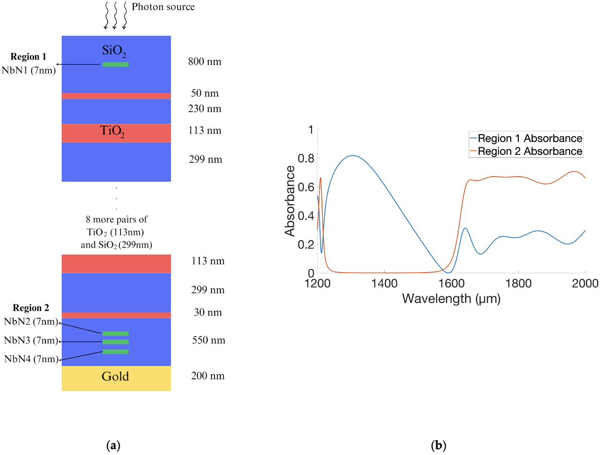
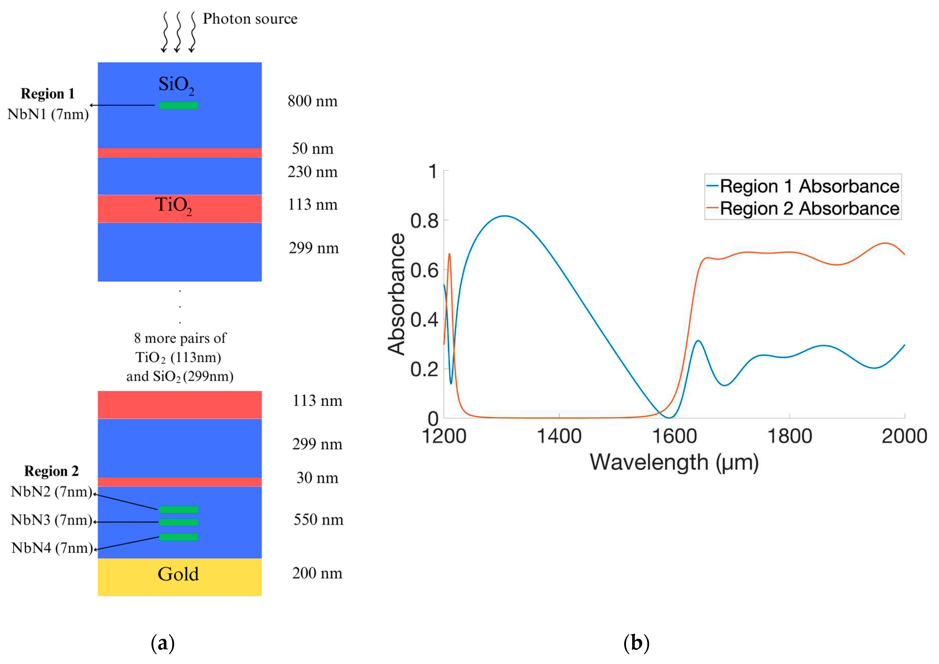
While this work describes a SNSPD design sensitive to photons with wavelengths ranging from 1070 to 2000 nm, it is important to note that this device is tunable. By changing the target wavelength of the DBR and placing the nanowires at the position with the strongest absorption resonance, it is possible to change the target wavelength of the SNSPD. For example, using the structure depicted in figure 7a, the simulated absorbance for Region 1 and Region 2 are shown in figure 7b.
Figure 7.
(a) Schematic of an alternative SNSPD design targeting different wavelengths; (b) The absorbance as a function of wavelength for Region 1 and Region 2 of the SNSPD.
Figure 7.
(a) Schematic of an alternative SNSPD design targeting different wavelengths; (b) The absorbance as a function of wavelength for Region 1 and Region 2 of the SNSPD.
5. Conclusions
In this work, we proposed a new dual-spectral SNSPD design, in which we stack a DBR on top of a gold mirror to achieve two distinct absorption bands. After tuning the thickness of the dielectrics and calculating the optimal positions for the nanowires, each nanowire positioned at those locations exhibits strong absorption resonance. By utilizing a modified DBR and a gold mirror as reflectors, the SNSPD design proposed in this work provides photon wavelength sensitivity in different tunable bands, opening up potential applications for future quantum communication technology.
Author Contributions
Conceptualization, P.W. and H.W.; simulation, P.W.; analysis, P.W., H.W., and S.P.; draft preparation, P.W.; manuscript review and editing, P.W., H.W., and S.P.; supervision, H.W. and S.P. All authors have read and agreed to the published version of the manuscript.
Funding
This research received no funding.
Institutional Review Board Statement
Not applicable.
Informed Consent Statement
Not applicable.
Data Availability Statement
Not applicable.
Conflicts of Interest
The authors declare no conflict of interest.
References
- Li, W.; Zhang, L.; Tan, H.; Lu, Y.; Liao, S.-K.; Huang, J.; Li, H.; Wang, Z.; Mao, H.-K.; Yan, B.; et al. High-rate quantum key distribution exceeding 110 Mb s–1. Nat. Photon- 2023, 17, 416–421. [Google Scholar] [CrossRef]
- Grünenfelder, F.; Boaron, A.; Resta, G.V.; Perrenoud, M.; Rusca, D.; Barreiro, C.; Houlmann, R.; Sax, R.; Stasi, L.; El-Khoury, S.; et al. Fast single-photon detectors and real-time key distillation enable high secret-key-rate quantum key distribution systems. Nat. Photon- 2023, 17, 422–426. [Google Scholar] [CrossRef] [PubMed]
- Shi, Z.; Wang, W.; Wu, X.; Yang, L. A Technique for Measuring Dynamic Slot-Power of Optical PPM Signals Based on SNSPD. IEEE Photon- Technol. Lett. 2022, 34, 1377–1380. [Google Scholar] [CrossRef]
- Guan, Y.; Li, H.; Xue, L.; Yin, R.; Zhang, L.; Wang, H.; Zhu, G.; Kang, L.; Chen, J.; Wu, P. Lidar with superconducting nanowire single-photon detectors: Recent advances and developments. Opt. Lasers Eng. 2022, 156. [Google Scholar] [CrossRef]
- Zadeh, I.E.; Chang, J.; Los, J.W.N.; Gyger, S.; Elshaari, A.W.; Steinhauer, S.; Dorenbos, S.N.; Zwiller, V. Superconducting nanowire single-photon detectors: A perspective on evolution, state-of-the-art, future developments, and applications. Appl. Phys. Lett. 2021, 118, 190502. [Google Scholar] [CrossRef]
- Gol’tsman, G.N.; Okunev, O.; Chulkova, G.; Lipatov, A.; Semenov, A.; Smirnov, K.; Voronov, B.; Dzardanov, A.; Williams, C.; Sobolewski, R. Picosecond superconducting single-photon optical detector. Appl. Phys. Lett. 2001, 79, 705–707. [Google Scholar] [CrossRef]
- Chang, J.; Los, J.W.N.; Tenorio-Pearl, J.O.; Noordzij, N.; Gourgues, R.; Guardiani, A.; Zichi, J.R.; Pereira, S.F.; Urbach, H.P.; Zwiller, V.; et al. Detecting telecom single photons with 99.5−2.07+0.5% system detection efficiency and high time resolution. APL Photon- 2021, 6, 036114. [Google Scholar] [CrossRef]
- Marsili, F.; Verma, V.B.; Stern, J.A.; Harrington, S.; Lita, A.E.; Gerrits, T.; Vayshenker, I.; Baek, B.; Shaw, M.D.; Mirin, R.P.; et al. Detecting single infrared photons with 93% system efficiency. Nat. Photon- 2013, 7, 210–214. [Google Scholar] [CrossRef]
- Reddy, D.V.; Nerem, R.R.; Nam, S.W.; Mirin, R.P.; Verma, V.B. Superconducting nanowire single-photon detectors with 98% system detection efficiency at 1550 nm. Optica 2020, 7, 1649–1653. [Google Scholar] [CrossRef]
- Omair, Z.; Hooten, S.; Yablonovitch, E. Optimized Optics for Highly Efficient Photovoltaic Devices. 2020 47th IEEE Photovoltaic Specialists Conference (PVSC), Calgary, AB, Canada, 15-21 June 2020; pp. 1813–1815. [CrossRef]
- Li, H.; Wang, H.; You, L.; Hu, P.; Shen, W.; Zhang, W.; Yang, X.; Zhang, L.; Zhou, H.; Wang, Z.; et al. Multispectral superconducting nanowire single photon detector. Opt. Express 2019, 27, 4727–4733. [Google Scholar] [CrossRef] [PubMed]
- Wang, H.; Hu, P.; Xiao, Y.; Zhang, X.; Zhou, H.; Zhang, W.; Li, H.; You, L.; Wang, Z. Multispectral Superconducting Nanowire Single-Photon Detector Based on Thickness-Modulated Optical Film Stack. IEEE Photon- J. 2022, 14, 1–4. [Google Scholar] [CrossRef]
- Li, H.; Wang, Y.; You, L.; Wang, H.; Zhou, H.; Hu, P.; Zhang, W.; Liu, X.; Yang, X.; Zhang, L.; et al. Supercontinuum single-photon detector using multilayer superconducting nanowires. Photon- Res. 2019, 7, 1425–1431. [Google Scholar] [CrossRef]
- Florya, I.N.; Korneeva, Y.P.; Mikhailov, M.Y.; Devizenko, A.Y.; Korneev, A.A.; Goltsman, G.N. Photon counting statistics of superconducting single-photon detectors made of a three-layer WSi film. Low Temp. Phys. 2018, 44, 221–225. [Google Scholar] [CrossRef]
- Salim, A.J.; Eftekharian, A.; Majedi, A.H. High quantum efficiency and low dark count rate in multi-layer superconducting nanowire single-photon detectors. J. Appl. Phys. 2014, 115. [Google Scholar] [CrossRef]
- Liu, D.; Miki, S.; Yamashita, T.; You, L.; Wang, Z.; Terai, H. Multimode fiber-coupled superconducting nanowire single-photon detector with 70% system efficiency at visible wavelength. Opt. Express 2014, 22, 21167–21174. [Google Scholar] [CrossRef]
- Gemmell, N.R.; McCarthy, A.; Liu, B.; Tanner, M.G.; Dorenbos, S.D.; Zwiller, V.; Patterson, M.S.; Buller, G.S.; Wilson, B.C.; Hadfield, R.H. Singlet oxygen luminescence detection with a fiber-coupled superconducting nanowire single-photon detector. Opt. Express 2013, 21, 5005–5013. [Google Scholar] [CrossRef]
- Li, H.; Chen, S.; You, L.; Meng, W.; Wu, Z.; Zhang, Z.; Tang, K.; Zhang, L.; Zhang, W.; Yang, X.; et al. Superconducting nanowire single photon detector at 532 nm and demonstration in satellite laser ranging. Opt. Express 2016, 24, 3535–42. [Google Scholar] [CrossRef]
- Xue, L.; Li, Z.; Zhang, L.; Zhai, D.; Li, Y.; Zhang, S.; Li, M.; Kang, L.; Chen, J.; Wu, P.; et al. Satellite laser ranging using superconducting nanowire single-photon detectors at 1064 nm wavelength. Opt. Lett. 2016, 41, 3848–3851. [Google Scholar] [CrossRef]
- Miao, W.-C.; Hong, Y.-H.; Hsiao, F.-H.; Chen, J.-D.; Chiang, H.; Lin, C.-L.; Lin, C.-C.; Chen, S.-C.; Kuo, H.-C. Modified Distributed Bragg Reflectors for Color Stability in InGaN Red Micro-LEDs. Nanomaterials 2023, 13, 661. [Google Scholar] [CrossRef]
- Lin, K.-C.; Lee, W.-K.; Wang, B.-K.; Lin, Y.-H.; Chen, H.-H.; Song, Y.-H.; Huang, Y.-H.; Shih, L.-W.; Wu, C.-C. Modified distributed Bragg reflector for protecting organic light-emitting diode displays against ultraviolet light. Opt. Express 2021, 29, 7654–7665. [Google Scholar] [CrossRef] [PubMed]
|
Disclaimer/Publisher’s Note: The statements, opinions and data contained in all publications are solely those of the individual author(s) and contributor(s) and not of MDPI and/or the editor(s). MDPI and/or the editor(s) disclaim responsibility for any injury to people or property resulting from any ideas, methods, instructions or products referred to in the content. |
© 2023 by the authors. Licensee MDPI, Basel, Switzerland. This article is an open access article distributed under the terms and conditions of the Creative Commons Attribution (CC BY) license (http://creativecommons.org/licenses/by/4.0/).
