1. Introduction
The critical role of the working electrode in electrochemical detection is underscored by the fact that all interested reactions take place on its surface. To facilitate diverse detection requirements, researchers have prepared working electrodes of various dimensions and compositions, including the Pt disk electrode, gold microdisk electrode, glassy carbon electrode, and so on. However, situations often arise necessitating the detection of two distinct subjects at the same time, prompting the utilization of a dual-working-electrode system.
Amongst the options for dual-working-electrode systems, the rotating ring disk electrodes (RRDE) stand as the most prevalent. Nonetheless, the utility of RRDE is circumscribed by its relatively modest collection efficiency, typically within the range of 20% to 40%, and large noise.1 In addition to RRDE, an alternative of Interdigitated Array (IDA) electrodes have drawn significant attention over recent decades.2-6
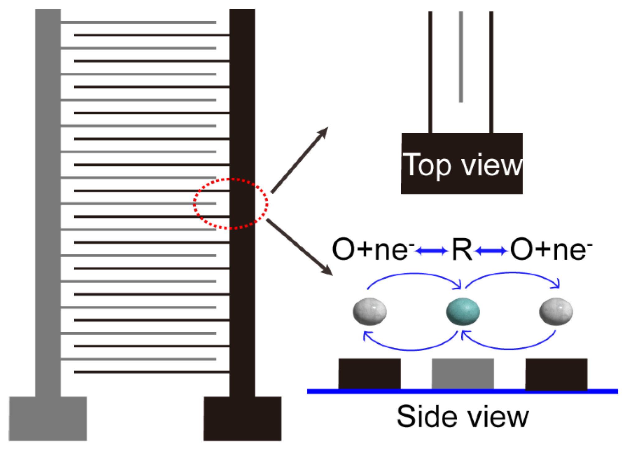
IDA electrodes are distinguished by their configuration, comprising two interdigitated comb-like working electrodes, denoted as the "generator" and "collector" in accordance with their functions (
Figure 1.)
7-9. This electrochemical tool's distinctive structure confers it with unique characteristics. Two distinctions when compared with RRDE worth particular attention: Firstly, the large increase of the number of electrode digits within IDA working electrodes, contrasting with the two working electrode digits in RRDE. Secondly, the noteworthy reduction in the size of these electrode digits, typically in the micron scale for IDA as opposed to the millimeter scale in RRDE. These distinctions yield two advantageous outcomes: (1) enhanced collection efficacy facilitated by the presence of numerous generator and collector arrays and (2) heightened efficiency in species mass transfer within the micron-scale electrode digits. Cumulatively, these attributes IDA electrodes a largely enhanced collection efficiency compared with RRDE.
In addition to the properties mentioned above, IDA exhibits a distinctive attribute due to its specialized structure, referred as the "feedback effect", which bears particular attention. Illustrated in
Figure 1., this phenomenon entails a mutual influence between the collector and generator currents. While the product generated by the generator is detected by the collector, this reaction does not culminate there; instead, the product from the collector disperses into the surroundings, works as the reactant for the generator reaction, and influences upon the generator current in turn. This recycling process generates a substantial amplification of the redox current signal, effectively functioning the IDA electrodes as a signal amplifier.
The micrometer-scale dimensions of IDA electrodes primarily engender diffusion as the predominant mode of mass transfer. This manifests two notable advantages: firstly, the electrochemical detection takes place within a quiet solution, characterized by mass transfer via diffusion rather than the convective forces induced by rotating electrodes. Consequently, this significantly diminishes noise levels while concurrently enhancing detection sensitivity. Secondly, the diffusion process toward the surroundings instigates the "feedback" effect mentioned earlier, functioning as a signal amplifier, and lowering the detection limits.10
The distinct structure of IDA permits the diffusion of products from the generator across the interelectrode spacing, wherein they can undergo the detection reaction at the collector. Researchers define the ratio of collector current to generator current as the collection efficiency (CE),4, 11-13 a pivotal metric for assessing IDA performance. Owing to the unique interdigital structure of IDA, the CE of IDA is much larger than that of RRDE.14, 15 Notably, IDA electrode width and electrode spacing are considered as critical determinants affecting redox cycling. Generally, CE is determined by the average diffusion distance (Width/4 + gap), with greater diffusion distances yielding reduced CE.4 Smaller spacings, conversely, permit the detection of transient intermediates. For instance, in research of oxygen reduction reaction, IDA electrodes find application in the detection of relatively unstable products such as hydrogen peroxide, thereby illuminating a two-electron-transfer reaction pathway. In contrast to alternative electrode types, IDA shows the advantages of heightened sensitivity, elevated current density, an amplified signal-to-noise ratio, and an expansive dynamic range.4
The functionality of IDA electrodes is highly influenced by both their dimensions and electrode material. Distinct sizes and materials suit specific application domains. IDA size predominantly hinges on the employed preparation method, which commonly encompasses photolithography16, 17, ink-jet printing18-20, direct laser writing21-23, and so on. Notably, IDA prepared via lithographic methods tend to be more diminutive in size while upholding heightened precision.
In light of the advancements achieved by IDA electrodes over three decades, these electrodes have drawn lots of attention and found applications in electrochemical analyses24-26, gas sensing27-29, micro-supercapacitors30-32, and beyond. This review will briefly introduce the fabrication of IDA electrodes, and the applications used by IDA electrodes.
2. Fabrications
Anticipation is directed towards two breakthroughs in the fabrication of IDA Electrodes: namely, the attainment of reduced dimensions and diversification in materials. Concerning size, the methodology employed during fabrication constitutes a critical determinant influencing the dimensions of IDA electrodes. Distinct fabrication techniques yield varying sizes and precision in IDA construction.
With regard to materials, the commonly used materials of IDA electrodes encompass gold, platinum, and carbon. Gold (Au) or platinum (Pt) IDA electrodes are typically favored for their relative ease of fabrication and good conductivity, so as to participate in a multitude of applications. Carbon, another noteworthy electrode material, is highly regarded in IDA applications owing to its favorable electrochemical properties, such as good stability, good conductivity, and a large potential window. The exploration of other non-metal materials, such as metal oxides, has also obtained attention, associated with distinct applications.
So far, reported fabrication methods for IDA electrodes mainly encompass photolithography,33-39 inkjet printing,20, 40 direct laser writing,41, 42 among others. Each of these preparation methodologies presents unique advantages. Researchers select an appropriate fabrication technique contingent upon the desired electrode dimensions and material. Consequently, this section shall integrate exemplar preparations from researchers, providing a comprehensive overview of three frequently employed IDA preparation techniques: photolithography, inkjet printing, and direct laser writing.
2.1. Photolithography
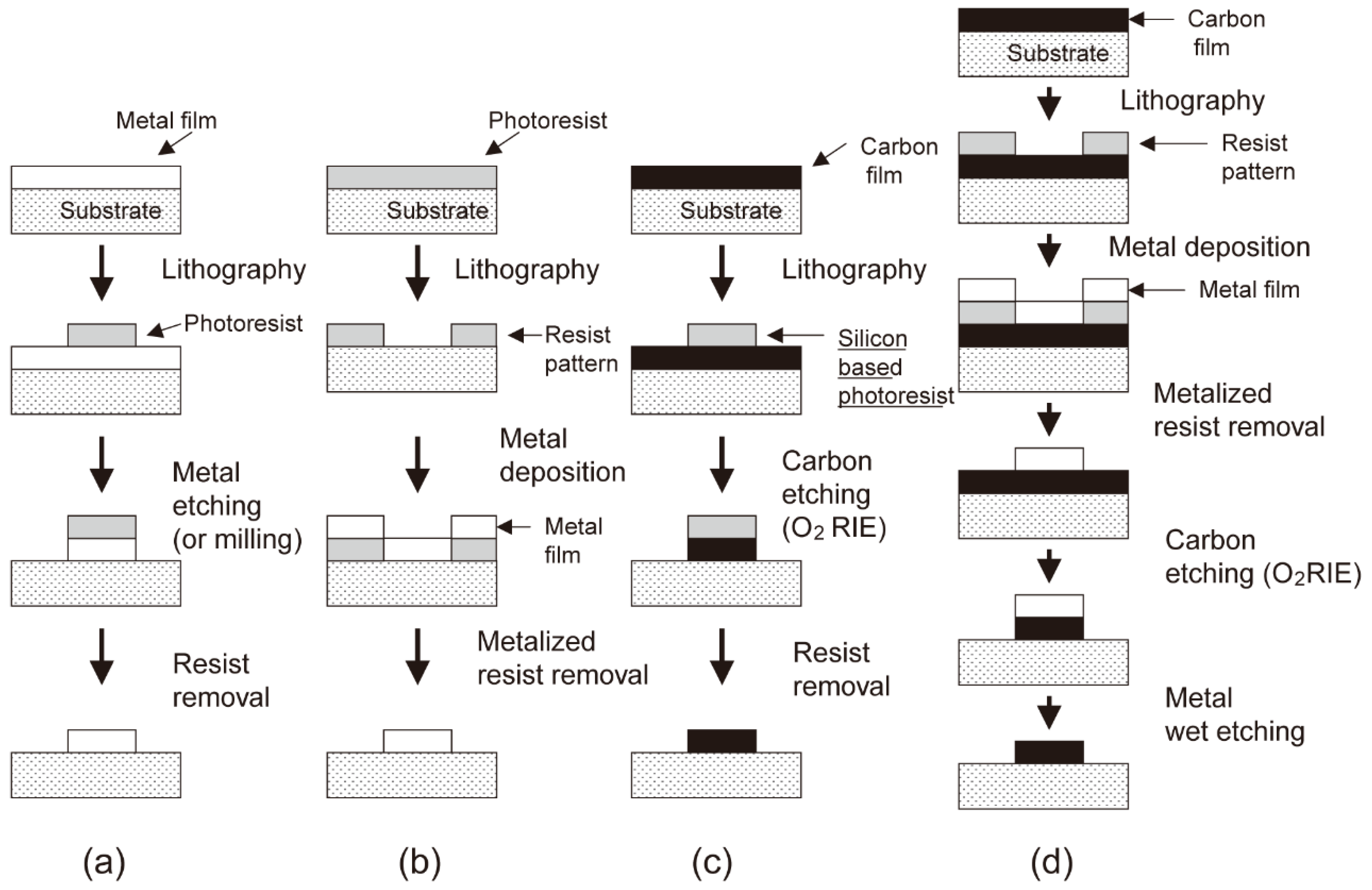
Photolithography stands as the predominant and widely employed method for the preparation of IDA electrodes, particularly in the preparation of metal-based IDA electrodes. Over the years, progress and refinements in photolithography techniques have established a mature platform for micron and nanofabrication. While it is worth noting that the specific parameters of IDA electrodes preparation via photolithography may exhibit variability across individual reports, the fundamental procedural framework remains the same, as described in
Figure 2.
33 In essence, the fabrication of the desired IDA pattern follows a series of steps: initially, the application of photoresist through spin coating, followed by exposure to light and subsequent development. Subsequent phases of the process involve the incorporation of distinct materials, such as carbon, gold, platinum, and others, to reach the specific requirements.
Lithography-based fabrication predominantly yields IDA electrodes ranging from several hundred nanometers to a few microns in size. In earlier studies, researchers focused their attention primarily on investigating the impact of electrode width and the electrode gap on IDA electrode performance. As the study has advanced, scholars have introduced the concept of 3D IDA, aiming at achieving enhanced redox cycling and enhanced collection efficiency. In addition to the dimensions of width and gap, recent research has studied the influence of microband height on electrode performance as well. This chapter mainly discusses the application of lithography technology in the IDA preparation process, so only the electrode size (width and gap) is considered and discussed from different lithography preparations.
The photolithographic fabrication process is notably straightforward when applied to metal-based IDA electrodes, primarily due to the well-established operations of liftoff and etching in the production of micron-scale metal structures. Conversely, the fabrication of carbon IDA (C IDA) electrodes presents considerably greater challenges compared with metal IDA. These challenges primarily stem from two key issues: first, the adhesion of carbon to the substrate is usually poor, and second, the liftoff and etching processes for carbon material fail to produce edges as precisely defined as those achieved with metallic materials. In the subsequent discussion, we will provide a comprehensive overview and comparative analysis of the fabrication for Au and Pt IDA electrodes versus C IDA electrodes.
2.1.1. Metal (Au, Pt) IDA
Metals, notably gold and platinum, are prominently favored for their advantages in serving as IDA electrodes. These attributes encompass excellent electrical conductivity, good biocompatibility, robust resistance to oxidation, and a relatively straightforward fabrication process even down to the nanoscale. Consequently, numerous scholars have undertaken the fabrication of diverse metal-based IDA electrodes on various substrates through photolithography techniques. The following sections will provide an exposition of the methodologies employed in the fabrication of metal IDA electrodes.
Peng Jin and colleagues
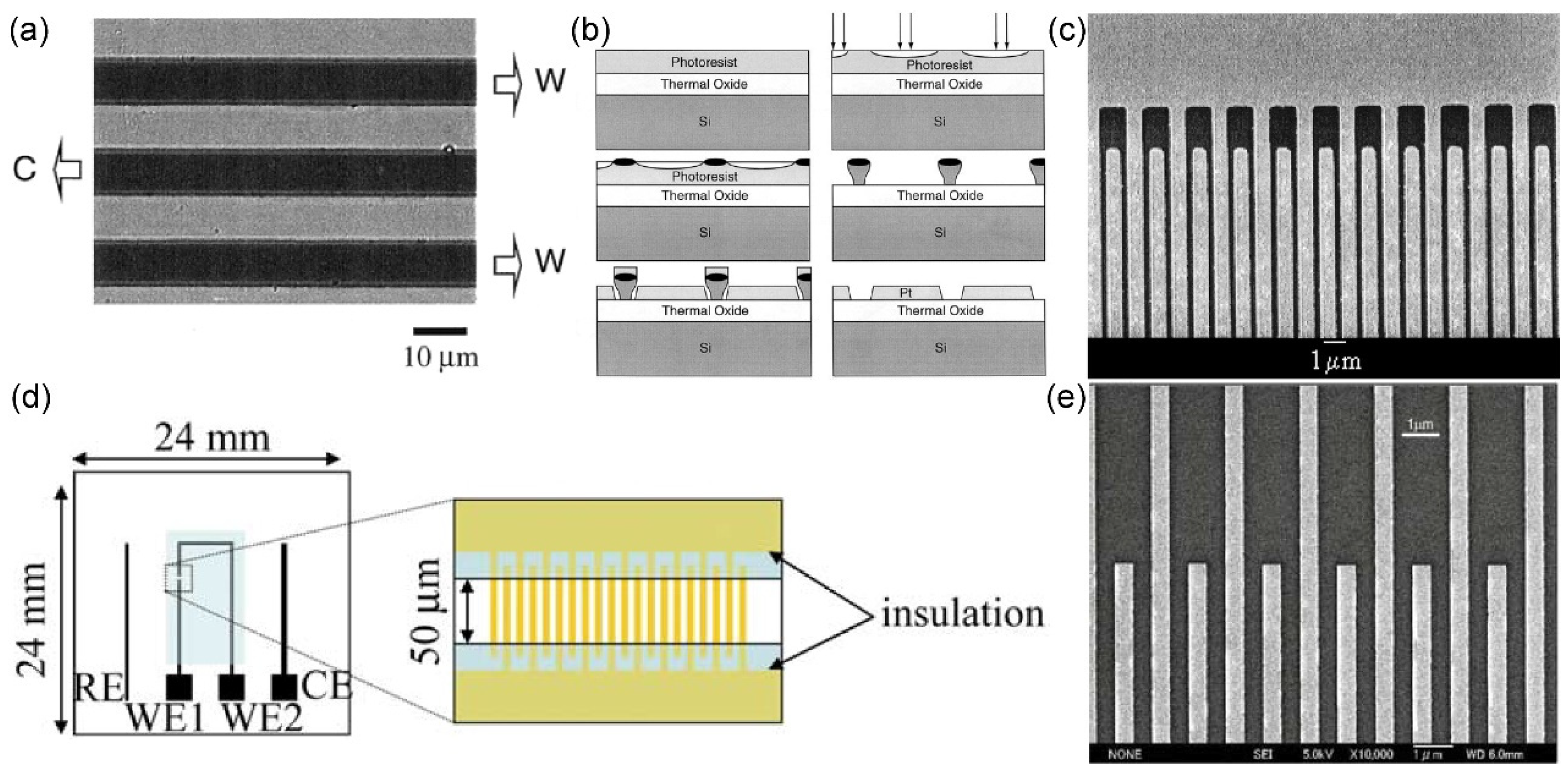
35 fabricated gold IDA electrodes with specific dimensions (width: 10 µm, gap: 10 µm) on a quartz substrate employing conventional photolithography techniques. The preparation process involved several steps. Initially, the quartz substrate underwent etching with 5% HF for 20 seconds, sonicated in acetone, methanol, and Milli-Q water for 5 minutes each. Subsequently, a layer of chromium (30 nm) and a layer of gold (350 nm) were deposited onto the substrate using a magnetron sputtering system. The photoresist (HPR-1183) is then spun onto the gold surface. This step involved a two-phase spin-coating process at speeds of 400 rpm for 5 seconds and 3000 rpm for 15 seconds. After completion of the spin coating, the substrate underwent a pre-baking step at 110°C for 4 minutes, followed by exposure to mid-UV light, post-baking at 90°C for 8 minutes, and development. Ultimately, the desired electrode structures were obtained.
Figure 3. (a) depicts the morphology of the IDA structure, as observed under a scanning electron microscope (SEM).
Adam E. Cohen and colleagues
34 successfully fabricated a collection of Pt IDA with excellent electrochemical properties through lithographic methods.
Figure 3. (b) provides an overview of the procedure. The methodology selects a silicon wafer as the substrate. A 500 nm-thick SiO
2 layer was grown through hot oxidation, followed by the spin-coating of a poly (vinyl phenol) layer. Subsequently, a photoresist layer underwent exposure through a 193-nm, 0.5-NA projection system. A 100 nm-thick Pt film was then deposited onto the silicon wafer through an evaporation process. The final step involved the removal of excess photoresist via a lift-off process, ultimately yielding the Pt IDA structure (
Figure 3. (c)).
Kosei Ueno and colleagues
36 employed a hybrid fabrication approach that combines photolithography and high-resolution electron beam (EB) lithography to fabricate nanoscale Au interdigitated array electrodes (Au IDA) with specific dimensions (width: 500 nm, gap: 500 nm) on a glass substrate (24×24 mm). In this process, a 2 nm-thick Ti layer was deposited via sputtering to serve as a binder, while a 70 nm-thick Au layer was applied as the electrode layer. Subsequently, precise IDA structures were fabricated using EB lithography, while larger patterns and bonding pads were generated through UV photolithography. The resultant configuration integrated the working electrode (Au IDA), counter electrode (Au), and reference electrode (Ag wire) onto the glass substrate, as illustrated in
Figure 3. (d). The morphological characteristics of the Au family of electrodes are depicted in
Figure 3. (e).
K. Reimer and collaborators
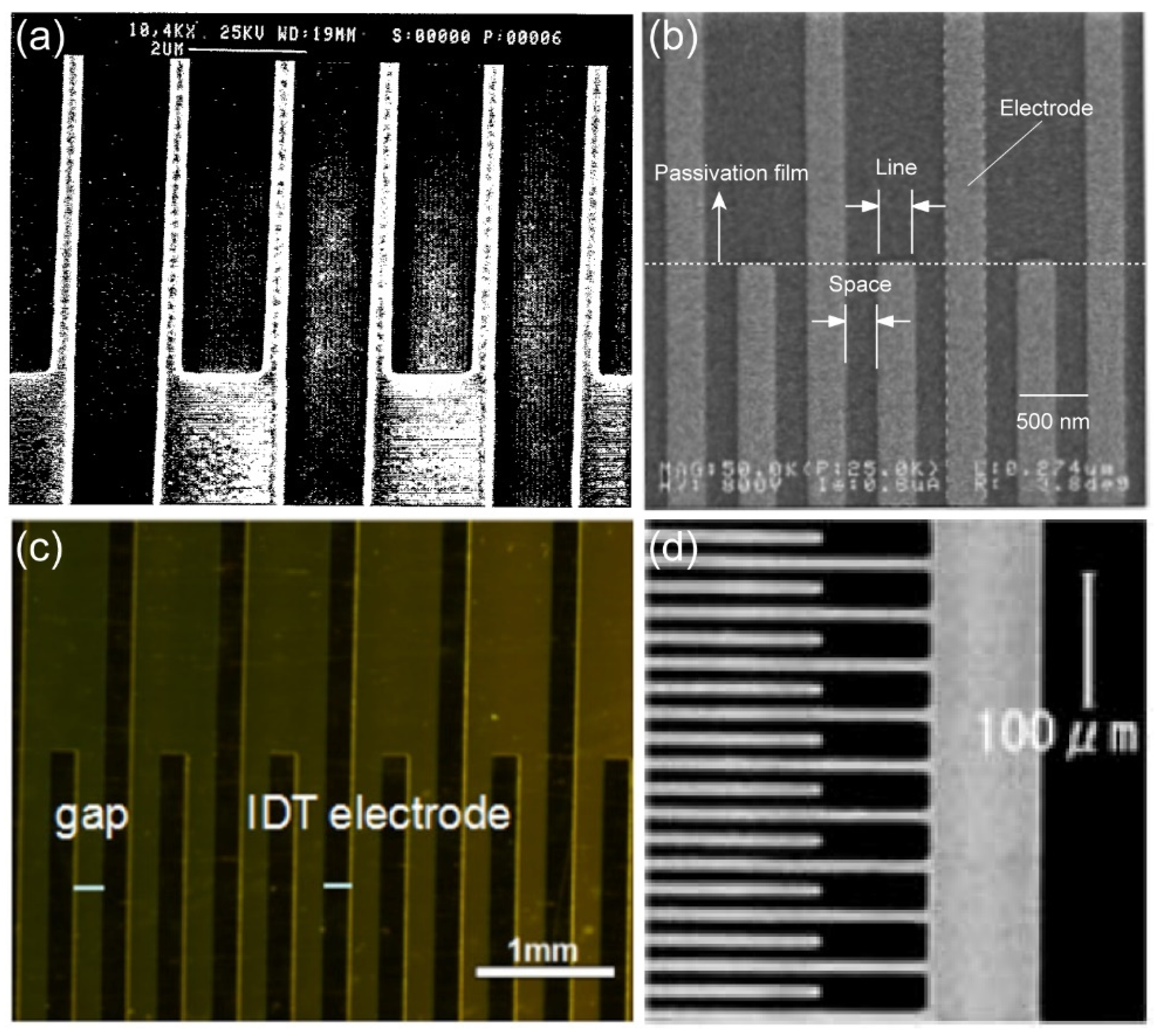
37 harnessed photolithography technique to fabricate metal IDA with small size. Remarkably, the gap of the metal IDA prepared by the group reached the nanoscale, where the gap of Pt IDA was only one-third of the width. Following the lithographic procedure, the research team executed a lift-off process and produced Pt IDA electrodes with specific dimensions (width: 1.5 µm, gap: 300 nm), as visually presented in
Figure 4. (a).
According to previous studies, Katsuyoshi Hayashi and collaborators
11 achieved a significant advancement in electrode size by successfully fabricating a metal IDA of nanoscale dimensions. They used photolithography technique to create Au IDA electrodes of nanoscale dimensions with both width and gap of 250 nm. (
Figure 4. (b)). Notably, the resulting Au nano-IDA demonstrated heightened sensitivity, particularly for biological detection. The diminutive size of these electrodes holds substantial promise for a wide array of applications, particularly in the domain of biosensing.
Jinzheng Gui and colleagues
38 embarked on the preparation of Au IDA on a polyimide substrate (PI) with a thickness of 50 µm. This strategic includes a combination of lithographic techniques and wet etching. The team first deposited an Au layer by magnetron sputtering on a PI substrate. Au IDA electrodes were obtained by standard lithography and wet etching. The electrodes they made contained a total of 41 Paris of microband electrodes, with an electrode width of 18 mm, a gap of 200 μm, as shown in
Figure 4. (c).
Hiroyuki Ojima and colleagues
39 prepared Pt IDA electrode (width:10 μm, gap:10 μm) by photolithography on a silicon wafer with a hot oxide layer. The methodological course commenced with the utilization of an L-350S-C machine (ANELVA, Tokyo) to execute the deposition of a titanium film onto the silicon wafer via sputtering. This titanium film served as a critical binder layer facilitating adhesion between the substrate and the subsequent metal electrode layer. Subsequently, a 0.1 µm-thick Pt film was sputtered onto the substrate, forming the electrode layer. The IDA structure was then crafted through a series of lithography steps, including the spin-coating of photoresist, pre-drying, and development. Following the completion of the fabrication process, SEM was employed for the purpose of morphological assessment of the resulting Pt IDA electrode, with the visual representation presented in
Figure 4. (d).
In conclusion, it is evident that the dimensions of IDA fabricated by various research teams exhibit considerable variability. This variability may be attributed to a multitude of factors, including the size of the mask plate employed, the type of photoresist selected, the thickness of photoresist applied during spin coating, UV exposure duration, and the temperature and duration of the baking process. Furthermore, we have undertaken a concise compilation of metal IDA characterized by diverse sizes, as outlined in
Table 1.
2.1.2. Carbon IDA
Despite the numerous favorable attributes of Au and Pt, their application in certain research contexts is constrained by their limited potential window. Specifically, this limitation is exemplified by the relatively narrow potential range within which reactions can be investigated. In contrast, carbon, being one of the most prevalent materials employed for working electrodes, offers excellent electrical conductivity, robust stability, and a notably expansive potential window. Consequently, researchers have explored the fabrication and examination of Carbon IDA (C IDA) electrodes.56 We provide a detailed account of C IDA preparation, aiming to provide a succinct explanation of the photolithography-based methodology employed for C IDA fabrication.
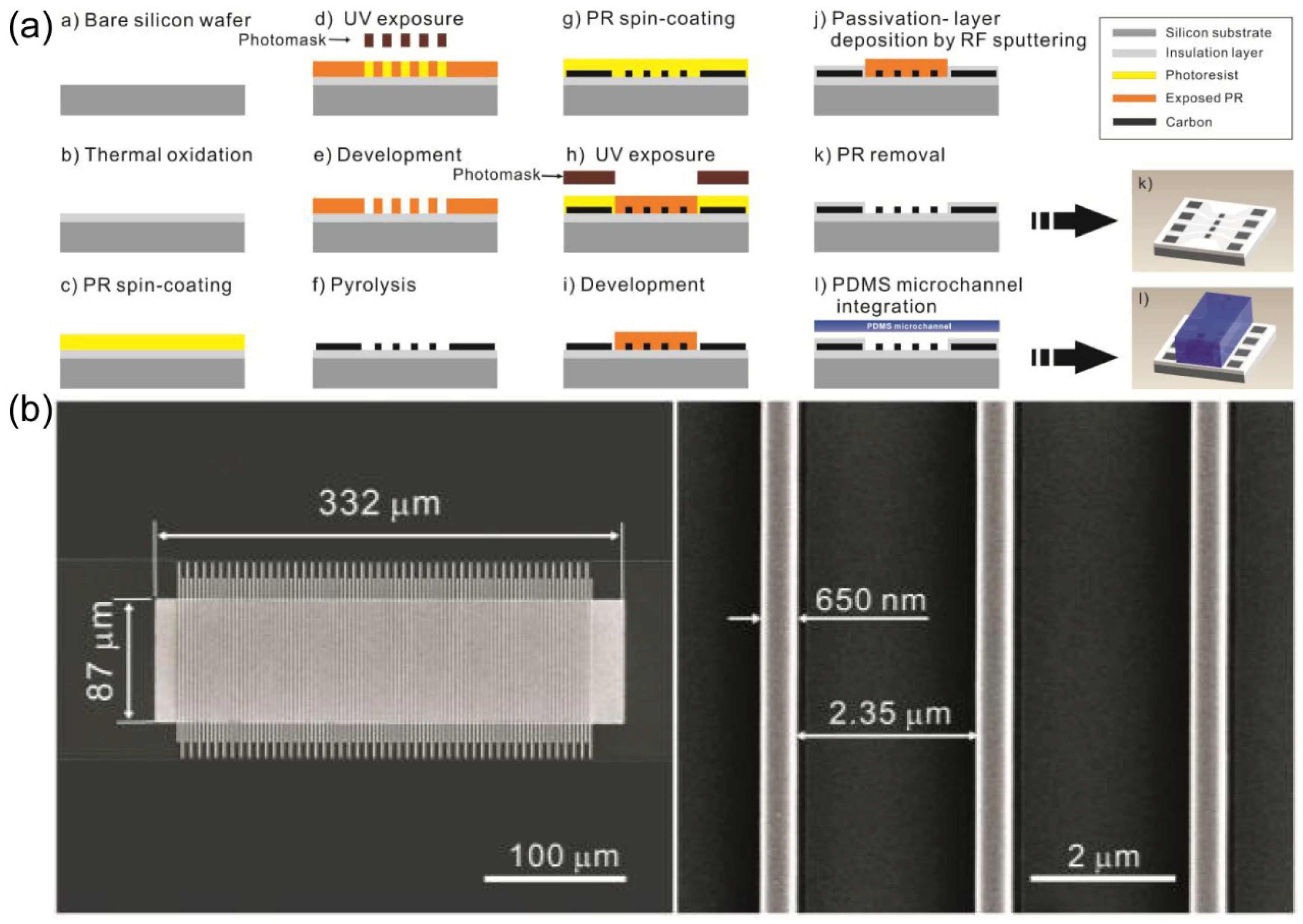
To investigate the amplification effect of redox cycling on current, Jeong-Il Heo and colleagues
57 embarked on the fabrication of nanoscale C IDA, characterized by specific dimensions (width: 650 nm, gap: 2.35 µm, thickness: 650 nm). This endeavor was realized through a combination of lithography technology and a pyrolysis process. The electrode preparation procedure, delineated in
Figure 5 (a), can be succinctly summarized as follows: initial treatment involving thermal oxidation of a silicon wafer and subsequent cleaning, spin-coating of photoresist (SU-8, Microchem, Corp., USA), the first photolithography process encompassing UV exposure, development, and pyrolysis, followed by another round of spin-coating photoresist, a second photolithography process, sputtering of a passivation layer, removal of the photoresist, and ultimately, PDMS packaging. The SEM characterization of IDA was shown in
Figure 5. (b). In chronoamperometry experiments, the redox current, derived from a 10 mM ferrocyanide solution, was remarkably amplified by a factor of 1116 times, courtesy of the deployment of a 650 nm thick, 650 nm wide, and 2.35 µm gap electrode pair within a 10 mm high channel.
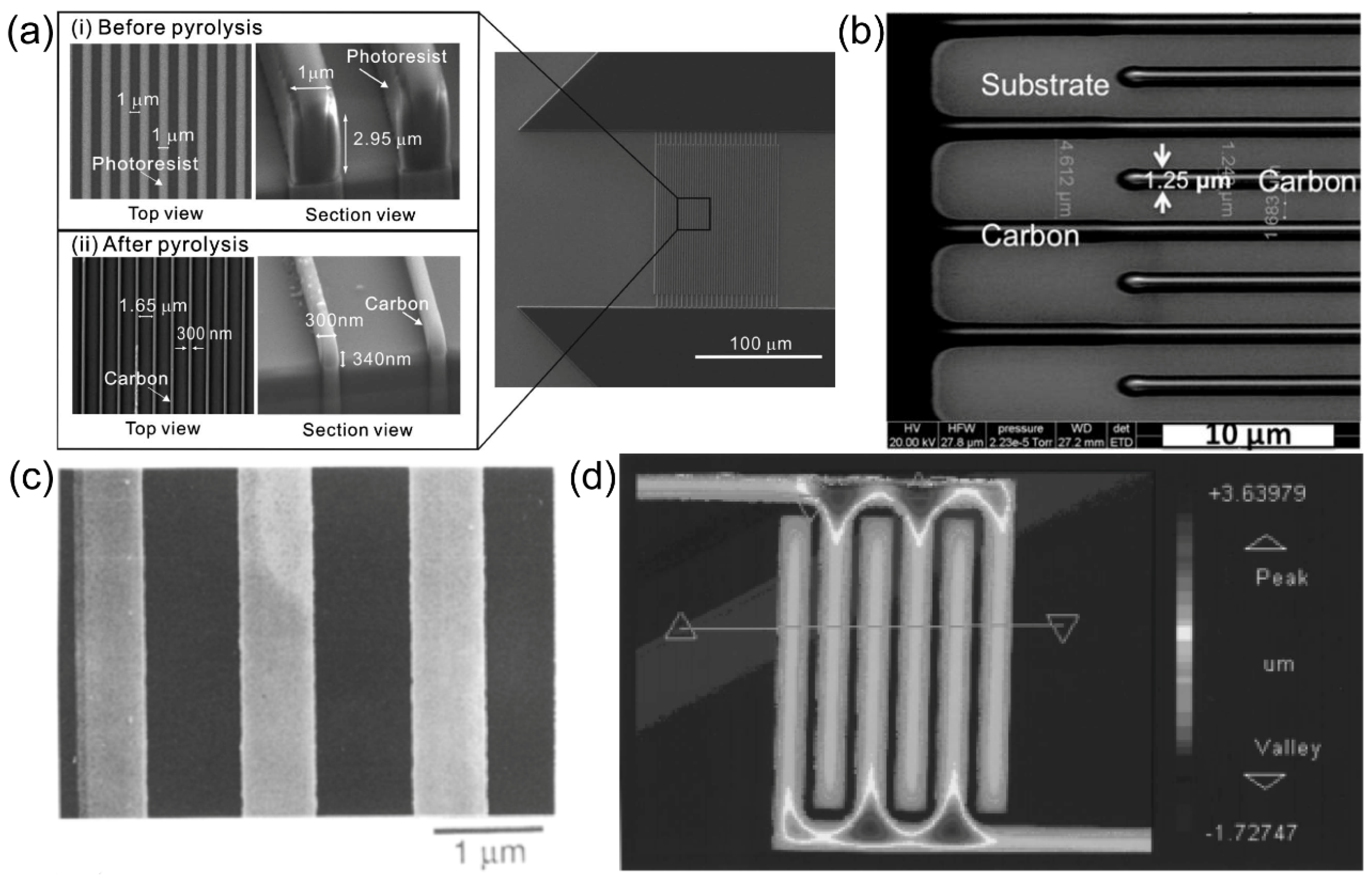
J. I. Heo and collaborators
9 achieved a significant reduction in the dimensions of C IDA, scaling them down to a submicron level. The methodology commenced with the utilization of lithography techniques to induce the formation of an IDA pattern within a 6-inch silicon wafer, with a silicon dioxide layer measuring 700 nm in thickness. Subsequently, the IDA underwent carbonization through heating in a vacuum environment, with the temperature reaching 900 ℃. During the pyrolysis process, it was observed that the photoresist experienced variable degrees of shrinkage in all directions, as visually depicted in
Figure 6. (a). To finalize the electrode configuration, the electrode leads were rendered inert via a 1 µm thick passivation layer of photoresist, exposing solely the interfingered regions. Notably, the C IDA electrodes exhibited the capability to amplify the redox current by a factor of 25, rendering them a cost-effective option for the construction of highly sensitive electrochemical detectors.
Fei Liu and colleagues
7 achieved successful preparation of C IDA with varying dimensions, specifically possessing widths ranging from 2 to 3 micrometers and gap ranging from 2 to 16 micrometers. The fabrication process involved initial treatment of the oxidized silicon wafer surface, followed by the deposition of a 1.5-micrometer-thick photoresist layer, employing photoresist materials such as S1813, AZS214E, and SU-8 2002. Subsequently, UV exposure was carried out utilizing a Mask Aligner. Following the exposure process, the electrode underwent heat treatment at 1000 °C, conducted under a controlled atmosphere comprising 5% H
2 and 95% N
2, with a heating rate of 2 °C per minute. This thermal treatment facilitated the gradual carbonization of the photoresist, ultimately leading to the formation of a carbon film. The SEM image is shown in
Figure 6. (b). Additionally, the research team conducted electrochemical assessments on the C IDAs generated using different types of photoresist materials, discerning that those fabricated with SU-8 exhibited better adhesion to the substrate.
Osamu Niwa and collaborators
58 achieved the successful fabrication of a C IDA series (width: 3 µm, gap: 2 µm), building upon the foundation of Pt-based electrodes. The fabrication process entailed the following steps: (1) Utilization of lithography to produce Pt IDA. (2) Electrochemical polymerization, involving the electroplating of a layer of polypyrrole (PPy) onto the surface of the Pt electrodes. The electroplating solution was primarily composed of 0.3 mol/L tetraethylammonium p-toluenesulfonate and acetonitrile, containing 1 mol/L pyrrole. Precise control over the quality of the PPy was maintained through the use of a digital coulomb meter. (3) Following the completion of the polymerization process, the Pt IDA electrodes, now featuring PPy films, underwent pyrolysis under vacuum conditions at 700℃ for a duration of 30 minutes. The morphological characteristics of the resulting C IDA post-pyrolysis are visually depicted in
Figure 6. (c). Notably, due to the pyrolysis process, the PPy gradually carbonized, ultimately forming a carbon film. This modification introduced a wider potential window to the Pt IDA, and its enhanced electrochemical activity was confirmed through substance measurements.
R. Kostecki and colleagues
12 adopted a conventional lithography and pyrolysis approach to fabricate C IDA. Notably, their approach differed from other research groups in that they took a custom approach to design and manufacture their mask plates. The general steps are outlined as follows: (1) Initiation with the design of the IDA pattern and mask design. (2) Following the mask plate design, the lithography steps paralleled those of other research groups, albeit with distinct parameter values. Specifically, the photoresist utilized was AZ-4330 (Hoechst Celanese), which underwent a soft baking process at 90℃ for 10 minutes. Notably, the pyrolysis process for carbon film production was conducted at 1000℃ for 1 hour, with a heating rate of 5 ℃/min. C IDA is shown in
Figure 6. (d).
To summarize the preparation process, we have provided a concise summary of C-film electrode fabrication in various research groups, as presented in
Table 2. Through an analysis of
Table 2 and the research conducted by the aforementioned group, it is apparent that the temperature at which the photoresist transforms into a C-film via pyrolysis may represent a significant influencing factor.
2.1.3. Other IDA
In addition to metal and carbon, some other materials, such as metal composite and metal oxide, have been prepared for various applications.
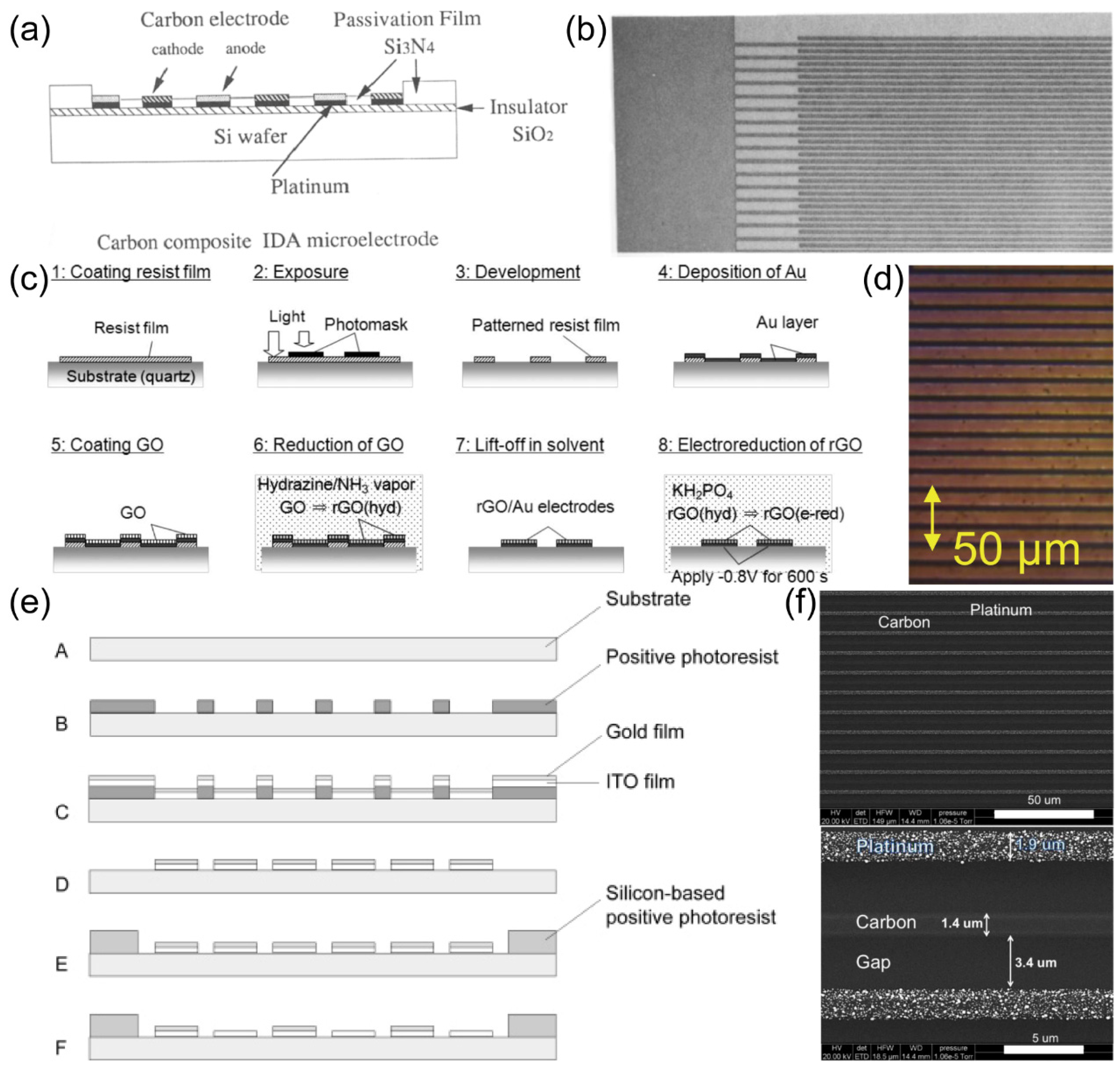
Hisao Tabei et al.
68 prepared a carbon/platinum composite IDA electrode (C/Pt IDA) with photolithography technique, in order to achieve the carbon property of wide potential window, as well as the metal property of good conductivity.
Figure 7. (a) was a schematic diagram of C/Pt IDA preparation process, general speaking, a Pt layer was deposited on SiO
2/Si substrate, then a carbon film was deposited on top of Pt, after that, the photolithography process was carried out and resulted in the designed IDA patterns on top of the carbon film. Then, the carbon film that not covered with resist was etched off, so as the Pt underlying. The wafer was then covered with silicon nitride film, then etched it until the carbon film is exposed. Finally, C/Pt IDA, which had 50 microband pairs of 3 μm width and 2 μm gap, was prepared. The structure diagram and SEM of C-Pt IDA electrode is shown in
Figure 7. (b). The excellent electrochemical performance of this C-Pt IDA electrode provides advantages for the analysis of reversible redox species, especially in the negative potential region of aqueous samples. The carbon film deposited on IDA electrode will be an excellent electrode material for constructing various thin film electrochemical cells.
Yuko Ueno et. al.
69 employed lithography techniques to fabricate IDA modified with reduced graphene oxide (rGO) and gold, aiming to enhance its electrochemical properties. Their successful synthesis of rGO-Au IDA electrodes involved a series of procedural steps on a 4-inch-diameter quartz substrate, including the application of photoresist, pre-heating at 80 ℃ for 60 minutes, ultraviolet exposure, gold layer growth via sputtering, and the deposition of an rGO film (
Figure 7. (c)). The surface morphology of the resulting electrode is depicted in
Figure 7. (d) as well. To optimize fluid measurement responses, this rGO-Au IDA was fabricated with reduced dimensions, boasting a width and gap of 2 µm each.
Katsuyoshi Hayashi and coworkers
70 employed lithography techniques to fabricate a series of IDA using indium-tin oxide (ITO) as the generator and gold as the collector. The electrode preparation process is shown in
Figure 7. (e). Glass wafers were used as the substrate, onto which a layer of positive photoresist (TSMR-V3, Tokyo Ohka Kogyo) was spin-coated, following pre-drying, exposure, and other essential steps. Subsequently, a 90 nm ITO film was sputter-deposited, followed by the addition of a 40 nm gold layer. The final IDA structure was realized using the lift-off method. Once the IDA electrode’s structure was prepared, the electrodes were immersed in a phosphate-buffered saline (PBS) solution to selectively remove the gold film from one side of the IDA electrodes.
Moreover, metal oxides also offer viable options as electrode materials, exemplified by titanium dioxide (TiO2). Fong Sze Yen and coworkers70 successfully fabricated TiO2-Al IDA electrodes on a silicon substrate. The process commenced with the deposition of an aluminum layer onto 2×2 cm silicon wafers through physical vapor deposition. Subsequently, the requisite IDA patterns were generated using lithography technology. The final step involved the application of a pre-prepared TiO2 solution onto the IDA's finger-like structures. Following five cycles of spin coating and a series of additional procedures including annealing, the TiO2-Al IDA electrode was attained.
Fei Liu and colleagues
2 employed a combination of photolithography and electrodeposition techniques to fabricate C-Pt IDA. Initially, C-C IDA were prepared using photolithography, a process detailed in their prior publication.
7 Subsequently, electrochemical deposition of Pt was conducted at the collector electrode of the C-C IDA. This electrochemical deposition process was carried out in a solution comprising 0.1 M HClO
4 and 2 mM K
2PtCl
6. To reduce Pt
4+ ions in the solution to elemental Pt at the collector electrode, a voltage range of 1.16V to -0.2V was applied, while the generator electrode remained open-circuited. This process was iterated over 8 cycles. Subsequent SEM characterization revealed the morphology of the successfully prepared C-Pt IDA electrodes, as depicted in
Figure 7. (f).
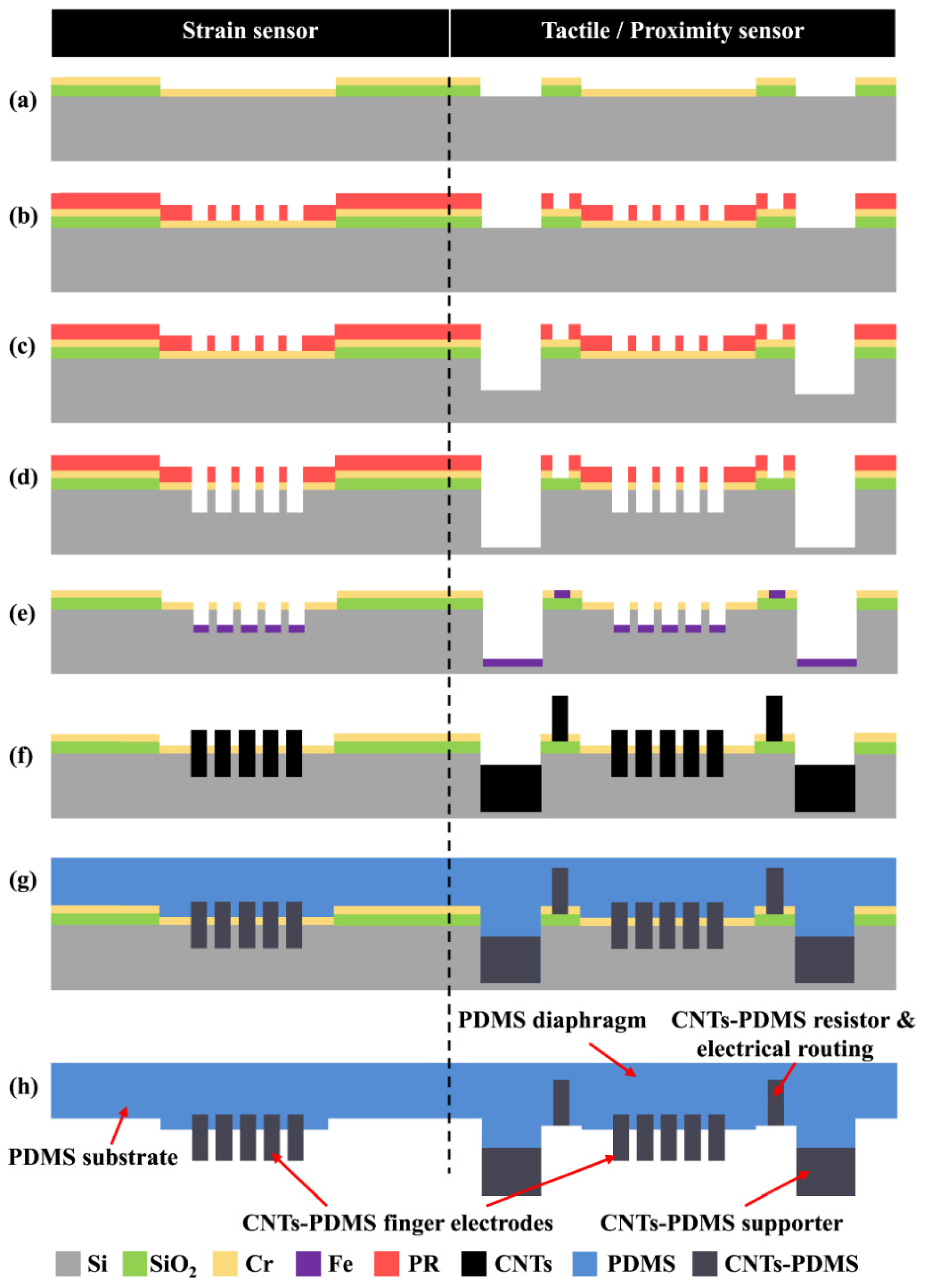
Chih-Fan Hu and colleagues
71 developed a composite sensor employing a 3D IDA structure. This study primarily outlines the fabrication procedure for Carbon Nanotube-polydimethylsiloxane (CNT-PDMS) IDA. The sensor's manufacturing process is visually depicted in
Figure 8. Initially, a layer of silica was deposited onto a silicon wafer, followed by the thermal evaporation of a chromium (Cr) film. Subsequently, a layer of photoresist was spun onto the substrate, exposed, and developed to create the IDA structure, as shown in
Figure 8 (a) and
Figure 8 (c).
Figure 8 (d) illustrates additional wet etching steps to eliminate the Cr layer. A 10 nm thick iron Fe film, acting as a catalyst for Carbon Nanotube (CNT) growth, was then deposited and patterned using the lift-off technique (
Figure 8 (e)). CNT growth was achieved via pyrolysis, resulting in a height of about 70 µm (
Figure 8 (f)). After growth, the 3D CNTs were encapsulated and covered with PDMS, followed by curing at 100 ℃ for 1 hour (
Figure 8 (g)). Subsequently, the CNT-PDMS IDA electrode was manually detached from substrate and transferred to a flexible PDMS substrate (
Figure 8 (h)). Post-preparation, SEM characterization was conducted, revealing clear evidence of CNT growth, as demonstrated in
Figure 9. (a).
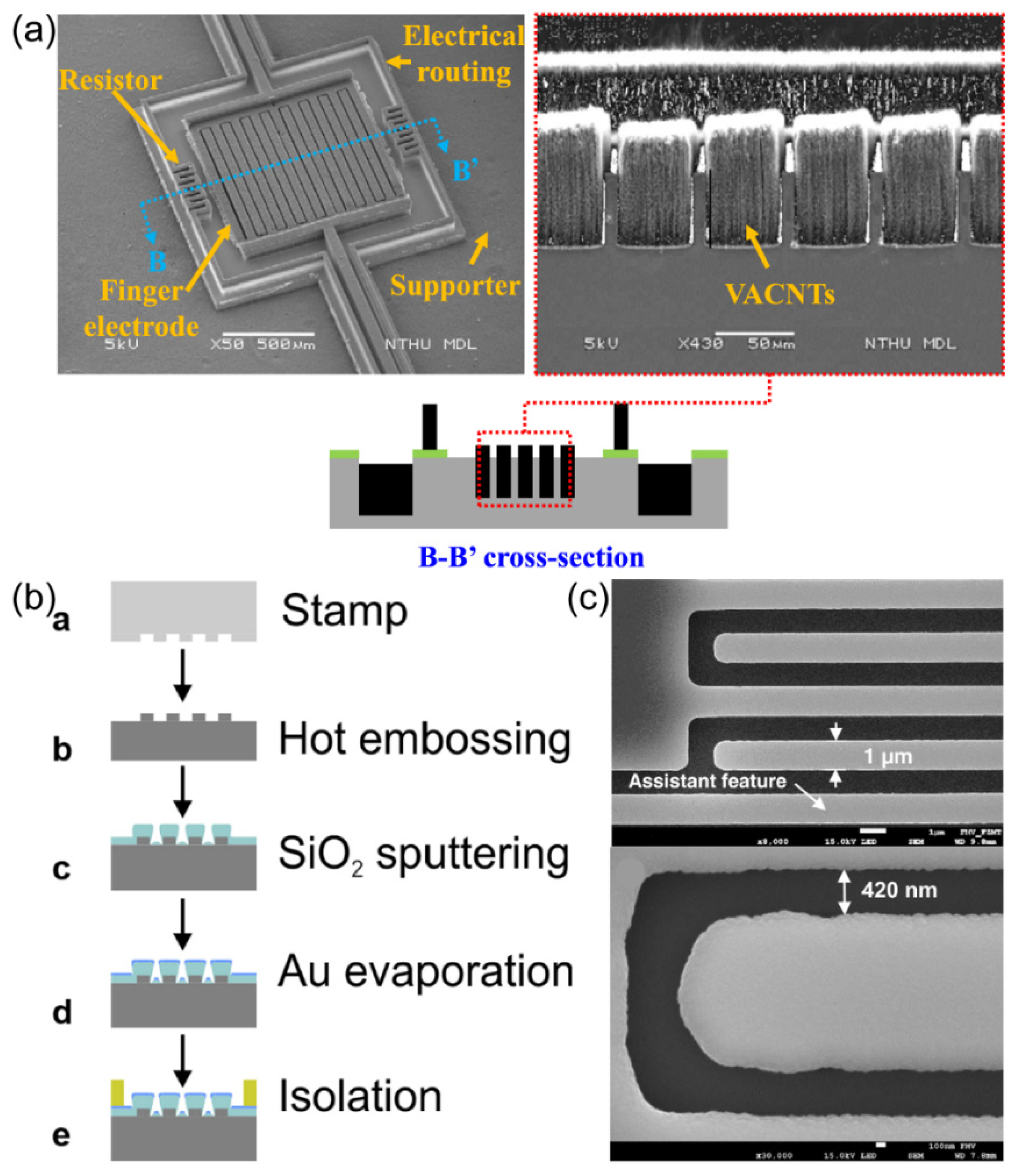
The majority of researchers use silicon wafers as their substrate when employing lithography techniques for IDA electrode fabrication. Conventional silicon-based IDA electrodes are costly, and the photolithographic preparation process is intricate. To address this, S. Partel and colleagues
72 have introduced an innovative method for preparing IDA electrodes on a polymer substrate, effectively reducing production costs.
Figure 9. (b) presents a schematic illustration of the IDA electrode preparation process on a polymer substrate. After the template featuring the IDA structure was generated via photolithography, this IDA pattern (width: 1 µm, gap: 420 nm) was transferred onto a 1 mm thick cycloolefin polymer (COP) sheet using a hot embossing technique. Subsequently, SiO
2 was deposited through sputtering, followed by the thermal evaporation of a 90 nm thick gold layer. The prepared IDA was characterized by SEM to obtain the morphology of the electrode surface, as shown in
Figure 9 (c). Electrochemical performance testing revealed that IDA electrodes prepared through this methodology exhibited the same capacity to amplify redox current signals as conventional silicon-based IDA electrodes.
In addition, the summary of electrode materials, substrates, photoresist and sizes used for the preparation of partial composite electrodes are shown in
Table 3.
2.2. Other methods
In addition to the commonly employed lithography technique, alternative methods such as inkjet printing and direct laser writing have found applications in the preparation of IDA electrodes.
Inkjet printing constitutes a non-contact printing process involving the precise deposition of ink droplets onto a printing medium to form images. Typically, inkjet printing operates through three primary modes: thermal inkjet, piezoelectric inkjet, and sonic inkjet. An illustrative example by Pattamon Teerapanich
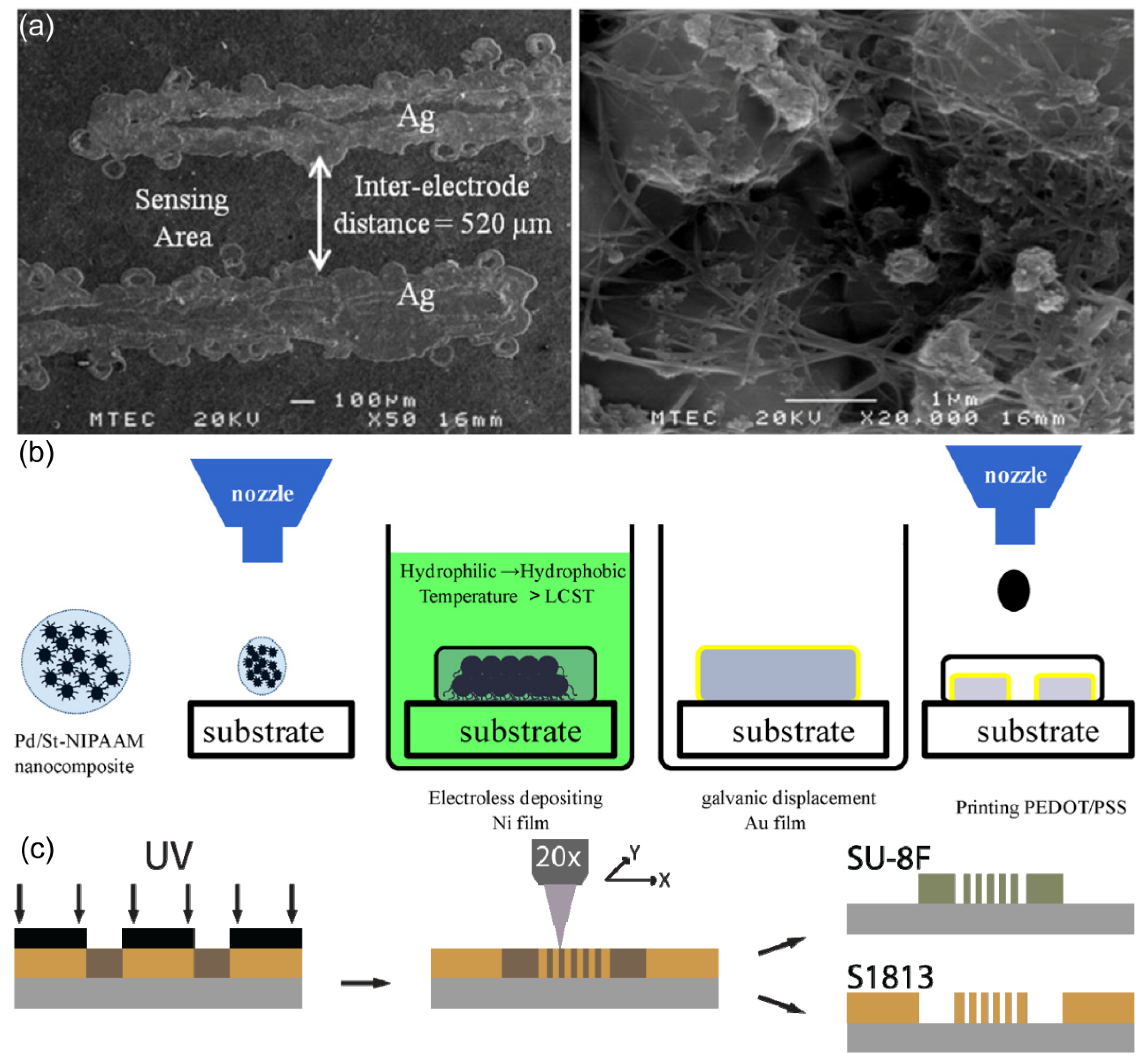
20 and colleagues demonstrates the use of inkjet printing to fabricate silver electrodes combined with single-wall carbon nanotubes (SWCNTs) for gas sensing applications at room temperature. Utilizing nanocolloidal silver as the ink medium, they generated Ag IDA structures on an aluminum substrate via inkjet printing. Subsequently, SWCNTs were grown between the electrode fingers, rendering the IDA suitable for gas sensor applications. The final IDA electrode exhibited specific dimensions: an electrode width of 0.18±0.01 mm, an electrode length of 1.97±0.01 mm, and an inter-electrode distance of 0.50±0.01 mm. The SEM image of the IDA electrode post-deposition is presented in
Figure 10. (a).
Chun-Chieh Tseng and colleagues
40 employed a novel approach by combining inkjet printing with electroless plating technology to create an innovative CO
2 gas sensor. The active layer of this sensor, poly(3,4-ethylenedioxythiophene)-poly(styrene-sulfonate) (PEDOT-PSS), was deposited onto Au IDA using inkjet printing. The process involved in modifying PEDOT-PSS onto the IDA electrode is elucidated in
Figure 10. (b). The primary focus of this study was directed towards the inkjet printing process for the active layer. To facilitate this, the researchers synthesized Pd nanoparticles via free radical polymerization and reduction reactions, subsequently formulating them into water-based inks (with a Pd concentration of 2 wt%). These inkjet-printed Pd nanoparticles served as a catalyst for subsequent Ni-P electroless plating. Following this, a gold film was electroplated onto the electrode surface through galvanic displacement. Ultimately, the ink was substituted with a PEDOT-PSS water suspension, enabling the inkjet printing of a PEDOT-PSS active layer onto the Au IDA electrode surface.
The Direct Laser Writing (DLW) technique, known for its non-contact and non-mask plate manufacturing process, offers advantages in terms of cost-effectiveness and flexibility. Despite its advantages, the utilization of DLW in the preparation of IDA electrodes has been relatively uncommon. Rajesh Kumar and colleagues41 applied DLW to fabricate IDA micro-supercapacitors. The IDA structure, featuring a width of 100 μm, a gap of 400 μm, a length of 5 mm, and comprising 19 pairs of electrodes, was generated using DLW on a free-standing ultra-thin graphite oxide (GO) film. In this process, the laser localized the reduction of graphite oxide, resulting in the formation of IDA structures with distinct conductivity compared to the substrate. DLW enabled the one-step production of miniature supercapacitors with graphene electrode patterns by simultaneously reducing and patterning graphene, leading to notable improvements in efficiency. These micro-supercapacitors produced via DLW exhibited high capacitance and excellent cycle stability.
Moreover, an intriguing approach was taken by Miles P. Lim and colleagues
42 who ingeniously integrated both direct laser writing and lithography techniques to complement each other's limitations. They initiated the process by exposing a photoresist using a cost-effective transparency mask with moderate resolution. Subsequently, direct laser writing was employed to generate smaller features, thereby eliminating the need for expensive and fixed masks employed in traditional lithography. This hybrid approach not only enhanced production speed when compared to using direct laser writing alone but also facilitated the formation of Interdigitated Array (IDA) patterns. Utilizing a negative photoresist (S1813), the team successfully crafted IDA patterns with a width of 2 μm. The final step involved the preparation of Au-IDA through thermal evaporation, lift-off, and other requisite processes, as illustrated in
Figure 10. (c).
2.4. Chapter summary
The currently reported fabrication methods for IDA electrodes predominantly encompass photolithography, inkjet printing, and direct laser writing techniques. Photolithography yields IDA electrodes with finer features and enhanced resolution in comparison to other methods. However, it is worth noting that photolithography entails a complex and costly process. On the other hand, inkjet printing offers a simpler and more straightforward patterning procedure, even though it has a lower resolution compared to traditional lithography. Direct laser writing, as the name implies, directly inscribes electrode patterns onto substrates, such as ultra-thin and flexible graphene oxide films, via laser processing. A distinctive advantage of direct laser writing is its freedom from mask plates, rendering it a more adaptable and cost-effective option. Nevertheless, it is important to acknowledge that direct laser writing may not achieve the same level of resolution as traditional printing and lithography processes.41
3. Application
As previously discussed, IDA electrodes show advanced characteristics such as heightened collection efficiency and sensitivity when contrasted with conventional dual-working electrodes. Their applications can be categorized into four domains, each aligned with specific application mechanisms. These domains encompass applications based on redox cycling, applications hinging on variations in IDA resistance and impedance, applications reliant on fluctuations in IDA capacitance, and device fabrication predicated on the unique structural attributes of IDAs.
3.1. Application based on redox cycling
Given the extremely close proximity, often at the micron or even nanometer scale, between adjacent microband electrodes, the diffusion layers of reactants and products exhibit partial overlap. Consequently, in the dual-mode operation of IDA, wherein one microband electrode is subjected to a specified potential range while the other is maintained at a constant potential, analytes undergo oxidation or reduction at the generator electrode. The resulting products diffuse toward the collector electrode, where they undergo reduction or oxidation. A fraction of the collector's product subsequently diffuses back to the generator electrode, actively participating in the ongoing reaction. These recurring processes involving reversible redox substances on IDA, characterized by such cyclic behavior, are referred to as "redox cycling". The schematic diagram of redox cycling principle of IDA electrode is shown in
Figure 1.
3.1.1. Neurotransmitters detection
Neurotransmitters, such as dopamine (DA) and adrenaline, play a pivotal role in transmitting information between neurons. Therefore, the precise measurement of neurotransmitter concentrations in biological fluids holds significant importance for the comprehensive study of neural activities, as well as early diagnosis and prevention of related disorders.75 Researchers have diligently devised multiple approaches for dopamine sensing, based on IDA electrodes and their exceptional efficiency, selectivity, and sensitivity3, 70, 76 The fundamental mechanism underlying these detection methods remains consistent: Utilizing redox cycling between the generator and collector electrodes to amplify the current signal, thereby functioning as a signal enhancer. Consequently, unidentified species, like dopamine, engage in repeated redox cycles between the generator and collector electrodes, resulting in an amplified output signal. This approach dramatically reduces the detection limit for dopamine. It's worth noting that different electrode materials and diverse modification techniques yield a spectrum of performances in dopamine sensing applications.
Masaya Takahashi et al.
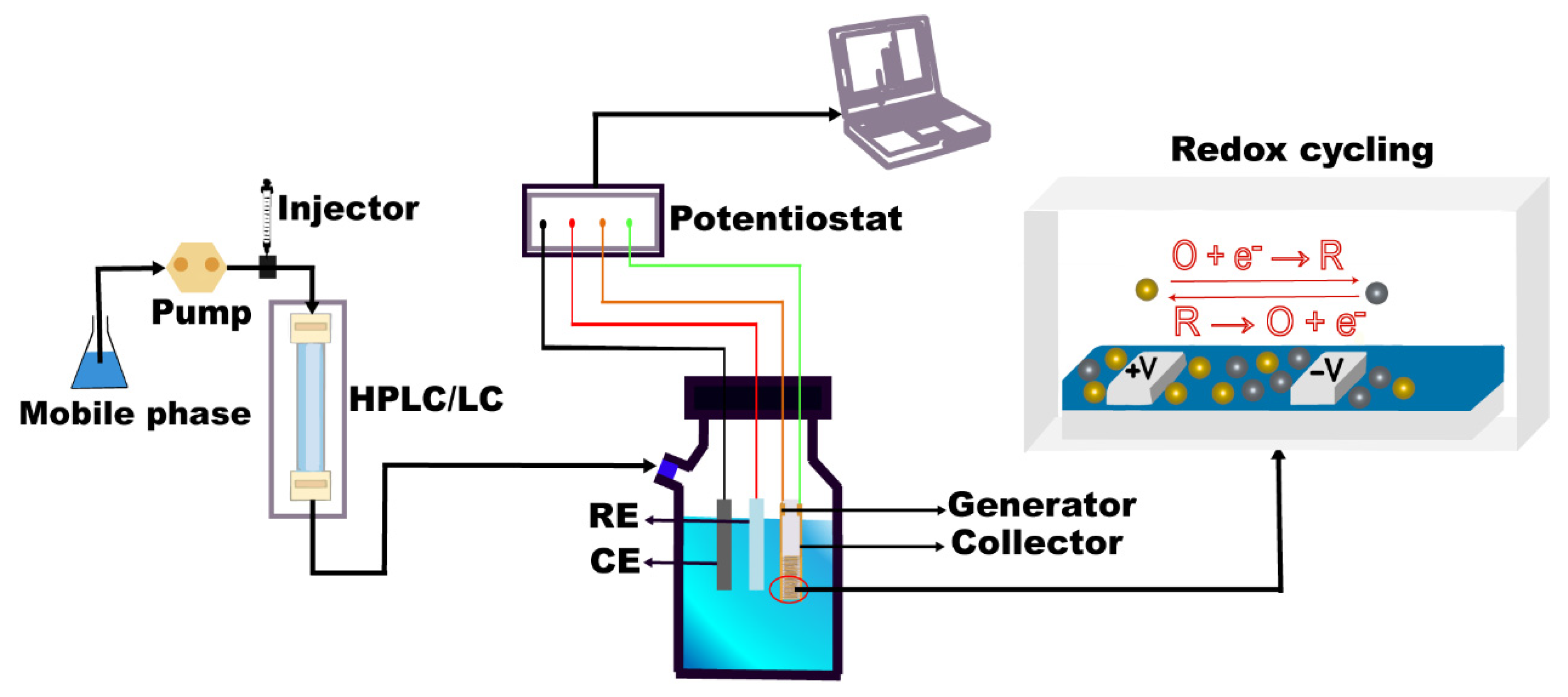
46 conducted a study involving the preparation and utilization of Au IDA as electrochemical detectors within the context of High-Performance Liquid Chromatography (HPLC) for the analysis of DA. The Au IDA exhibited a microband configuration with a width and spacing of 2 μm each. According to the description of the research group, we drew a schematic diagram of the application principle of Au IDA in HPLC, as shown in
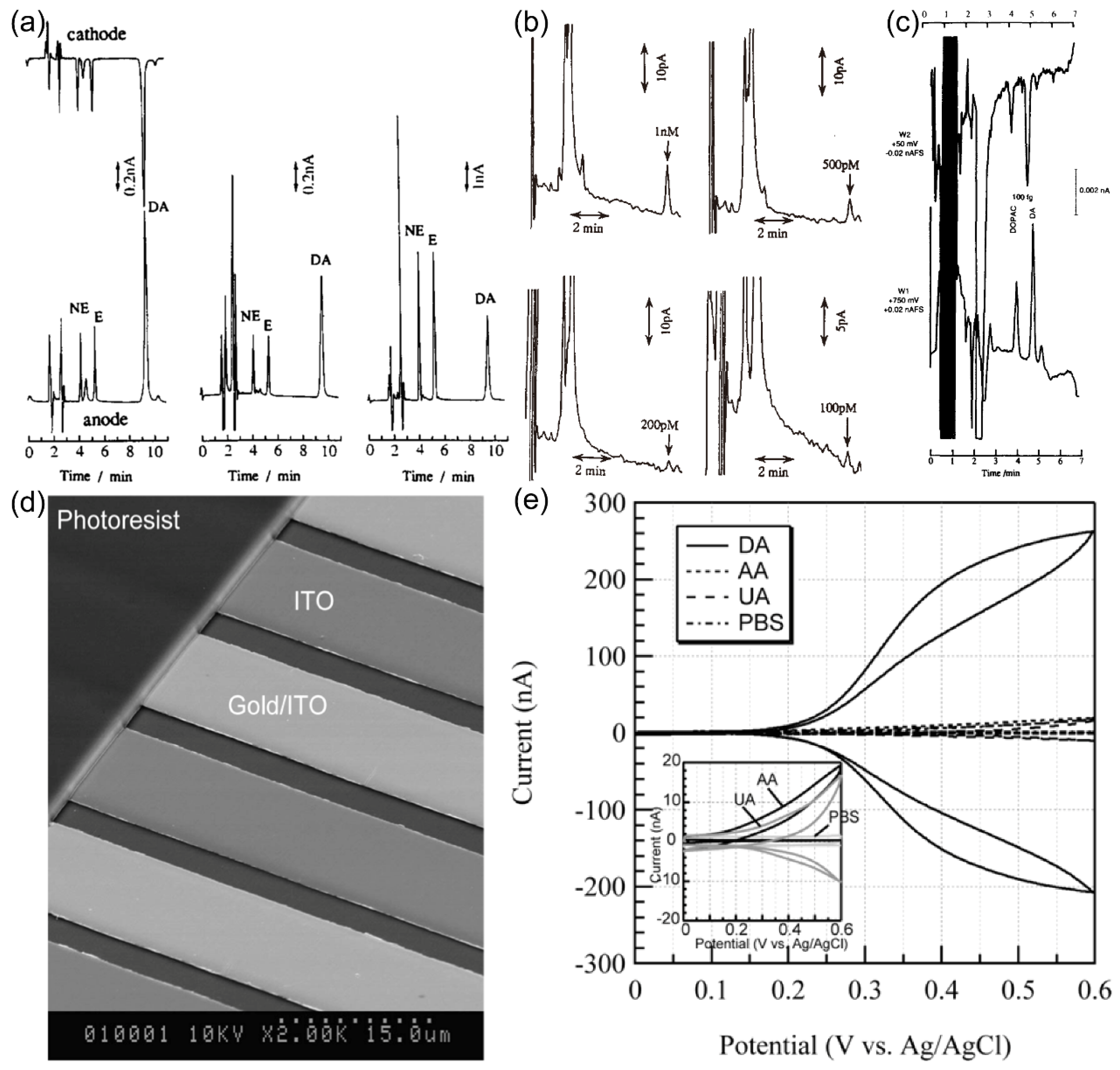
Figure 12. The research team conducted experiments involving DA, epinephrine (E), and norepinephrine (NE), both in single and dual IDA electrode modes combined with HPLC. As the sample flow traversed the cell channel, it underwent reactions on the IDA electrodes, benefiting from the "redox cycling" phenomenon, ultimately yielding amplified current signals. The results, illustrated in
Figure 13. (a) revealed distinct disparities in DA signals compared to those of E and NE. This distinction stemmed from DA's unique ability to undergo reversible conversion between the generator and collector electrodes, significantly enhancing the response signal, as demonstrated in
Figure 11. Various DA concentrations were investigated, with the current peak of DA distinguishable from baseline noise, even at concentrations as low as 100 picomolar. (
Figure 13. (b)) This underscores the Au IDA electrode's excellent sensitivity to DA, low noise levels, and high peak current density when employed as an electrochemical detector in HPLC applications.
The utility of Au IDA in negative potential applications is constrained by the narrow potential window of Au within the cathodic region. Recognizing carbon as an optimal material for working electrodes due to its enhanced stability and broader potential window, Osamu Niwa et al.
3 fabricated C IDA electrodes, characterized by a width, gap, and length of 2 micrometers each and 2 millimeters, respectively. These electrodes were then integrated with a 1-millimeter microporous column to facilitate the detection of DA through liquid chromatography (LC). The schematic diagram of the combination of IDA and LC is shown in
Figure 12. The redox cycling of IDA was related to the mobile phase's flow rate, with a larger redox cycling observed at lower flow velocities. The utilization of a 1 mL microporous column contributed to heightened sensitivity compared to conventional columns, as analytes within the column experienced less dispersion, and the flow rate was typically slower. The results indicate that the IDA electrode's limiting current exhibits a proportionate relationship with the cubic root of the flow rate.
Figure 13. (c) illustrates a chromatogram capturing the measurements of DA and 3,4-dihydroxyphenylacetic acid (DOPAC) using a C IDA. With a flow rate of 70 microliters per minute, a 5-microliter sample containing 0.65 femtomoles of DA and 0.59 femtomoles of DOPAC yielded peak currents of 6.2 picoamperes and 3.2 picoamperes, respectively. Subsequent calculations and data processing revealed detection limits of 5.0 femtograms for DA and 9.6 femtograms for DOPAC. Consequently, the coupling of C IDA with microbore LC for DA detection demonstrated exceptional sensitivity. In comparison to alternative sensors, this C IDA exhibited remarkably low detection limits for both DA and DOPAC.
The previously mentioned Au IDA
46 and C IDA
3 are not suitable for the detection of analytes in biological fluids in the presence of electroactive interferents, such as ascorbic acid (AA) and uric acid (UA). In response to this challenge, Katsuyoshi Hayashi et al.
70 introduced a novel IDA detector variant, denoted as hetero ITO-Au IDA electrodes. Notably, the incorporation of indium tin oxide (ITO) into the electrode design serves to attenuate the response of UA and AA, and additionally mitigates the reduction of DA oxidation byproducts. Consequently, this innovation enables selective redox cycling and signal amplification of DA. Specifically, ITO functions as the IDA generator (oxidation reaction), while Au serves as the IDA collector (reduction reaction). The Au electrode efficiently mediates the reduction of DA oxidation products, thereby facilitating redox cycling exclusively involving DA between the ITO generator and Au collector. The microband configuration of this ITO-Au IDA electrodes have a 10 μm width and a 5 μm gap, as depicted in
Figure 13. (d). Subsequent to device fabrication, the research team prepared a standard sample solution using phosphate buffer saline (PBS) and conducted cyclic voltammetry analyses of AA, UA, and DA, as illustrated in
Figure 13. (d). Evidently, the response signals of AA and UA are substantially suppressed, while the signals corresponding to DA exhibit pronounced enhancement. By obviating the need for the separation of electroactive interferents, the ITO-Au IDA allows for the continuous monitoring of DA, thereby facilitating real-time monitoring of catecholamines in bodily fluids.
A lot of research efforts have been dedicated to the detection of DA using IDA electrodes, with a compilation of pertinent studies presented in
Table 1. Notably, the outcomes of these detections are influenced by factors such as electrode material, electrode dimensions, and the employed detection methodology. C IDA electrodes have prominently featured in the array of sensors designed for DA detection.
Table 4.
A Summary of other studies on DA detection using IDA electrodes.
Table 4.
A Summary of other studies on DA detection using IDA electrodes.
| detector |
detection method |
detection result |
Ref |
| Au IDA(width: 2 μm, gap: 2 μm) |
high performance liquid chromatography |
DA detection limit: 100 pM |
46 |
| ITO-Au IDA(width: 10 μm, gap: 5 μm) |
cyclic voltammetry |
the sensitivity of AA and UA were 6% and 5% that of DA. |
70 |
| C IDA(width: 2 μm, gap: 2 μm) |
Liquid chromatography with microporous columns |
DA detection limit: 5.0 fg
DOPAC detection limit: 9.6 fg |
3 |
| C IDA (width: 2 μm, gap: 2 μm) |
liquid chromatography |
DA detection limit: 5 fg (32 amol) |
78 |
| C IDA(width: 650 nm, gap:2.35 μm) |
cyclic voltammetry |
DA detection limit: 10 μM |
57 |
| C IDA(width: 3 μm, gap: 2 μm) |
cyclic voltammetry |
DA detection limit: 10 nM |
79 |
3.1.2. Biological protein detection
Immunoassay serves as a prevalent diagnostic modality in the medical field, facilitating the identification of various immune-related disorders, including immunodeficiency diseases, viral infections, malignant tumors, and more. It plays an important role in dissecting the underlying disease mechanisms, consequently aiding in the formulation of medical intervention strategies. A central focus of this research involves signal amplification for immune detection. Among these, enzyme labeling emerges as a widely adopted method due to its capability to transform non-electrochemically active substrates into electrochemically active products via enzymatic reactions. This transformation towards enhanced electrochemical detectability significantly enhances the sensitivity of immune sensing. Utilizing the properties of IDA electrodes, which facilitate the reversible redox cycling of substances, numerous research teams have successfully engineered high-performance immunosensors.
Osamu Niwa and colleagues
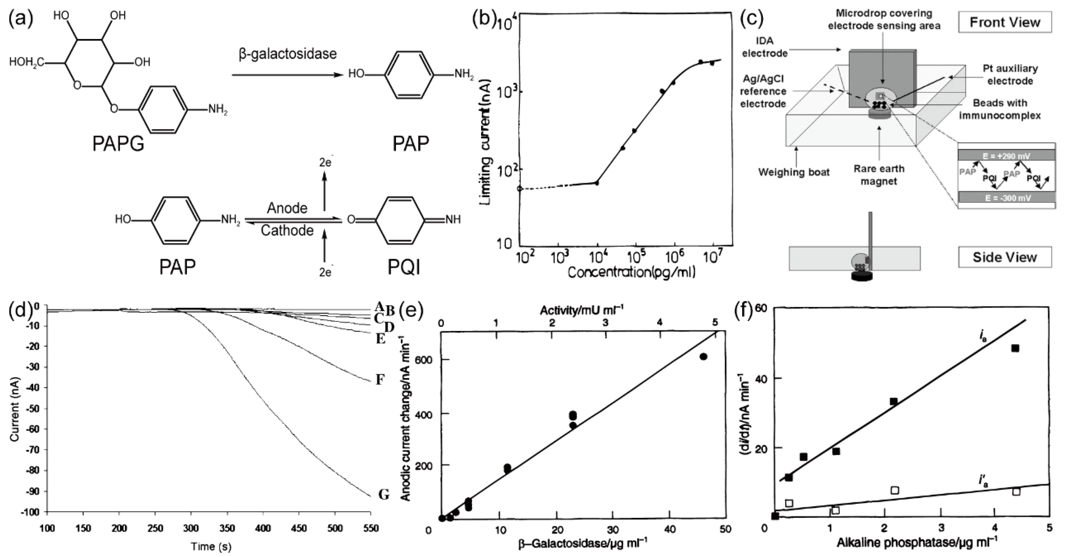
27 conducted an electrochemical enzyme immunoassay by fabricating Au IDA electrodes with specific dimensions (width: 3 μm, gap: 2 μm) using lithographic techniques. In this immunoassay, alkaline phosphatase served as the enzyme label. The fundamental principle involved assessing the concentration of mouse IgG by quantifying the levels of p-aminophenol (PAP), which were catalytically generated by alkaline phosphatase from a substrate known as 4-aminophenyl phosphate (PAPP). Within this electrochemical context, PAP, a reversible redox material, underwent oxidation to form 4-quinone imine (PQI) at a potential of 290 mV (vs. Ag/AgCl). The reaction equation is shown in
Figure 14. (a). Importantly, the PAP/PQI redox couple exhibited the capacity for redox cycling on the Au IDA electrode, leading to a more robust current output signal. The electrochemical measurements were conducted using cyclic voltammetry (CV), wherein the generator potential underwent cycling between -0.3V to 0.3V (vs. Ag/AgCl), facilitating reactions between PAP and PQI. Simultaneously, the collector potential remained fixed at -0.3V (vs. Ag/AgCl) to effectuate the reduction of PQI back to PAP. The resultant relationship between cathodic limiting current and IgG concentration is shown in
Figure 14. (b). Remarkably, this immunoassay exhibited a testing range for mouse IgG spanning from 10 to 1000 ng/mL, with a detection limit as low as 10 ng/mL.
Jennifer H. Thomas et al.
45 engineered a Pt IDA electrode with specific dimensions, prepared at the Micro-Electro-Mechanical Systems (MEMS) facility situated within the Georgia Institute of Technology. The IDA electrode exhibited the width of 2.4 μm, the gap of 1.6 μm, and 25 pairs of microbands. A schematic representation of experimental setup can be observed in
Figure 14. (c). In this study, mouse IgG was the analyte, while β-galactosidase served as the enzyme label. To maintain a fixed distance from the electrode surface, microbeads were magnetically immobilized at the base of a weighing boat. These microbeads functioned primarily as solid support entities for the immunoassay. Notably, their small size facilitated expedited diffusion of enzymatic reaction products towards the electrode surface, thereby accelerating the reaction process. The reaction mechanism is illustrated in
Figure 14. (a). Subsequently, the research team conducted electrochemical assessments across varying concentrations of mouse IgG, yielding the resultant current response signal, as depicted in
Figure 14. (d). Impressively, the analysis detected the signal emanating from 1000 microbeads within a 20 μl sample droplet in under 10 minutes. Furthermore, the detection threshold for mouse IgG was established at 50 ng/mL.
As illustrated in
Figure 6, it is evident that the generation of p-aminophenol glucuronide (PAPG) involves the catalytic influence of alkaline phosphatase (ALP) and β-galactosidase. Consequently, the quantification of PAP concentration not only facilitates the assessment of IgG concentration but also provides valuable insights into the enzymatic activity of ALP and β-galactosidase. Ulla Wollenberger and colleagues
52 undertook the fabrication of Pt IDA with a width of 3.2 μm, a gap of 0.8 μm, and an overall length spanning 900 μm. Notably, PAP possesses diffusion layers with thicknesses akin to the dimensions of the gap, thus making the radial diffusion as the predominant mass transfer mechanism. This intrinsic characteristic confers remarkable sensitivity upon Pt IDA for the detection of PAP concentration. The results of their experiment are presented in
Figure 14. (e).and
Figure 14. (f), revealing impressively low detection limits of 0.5 pmol and 0.1 pmol for β-galactosidase and ALP, respectively.
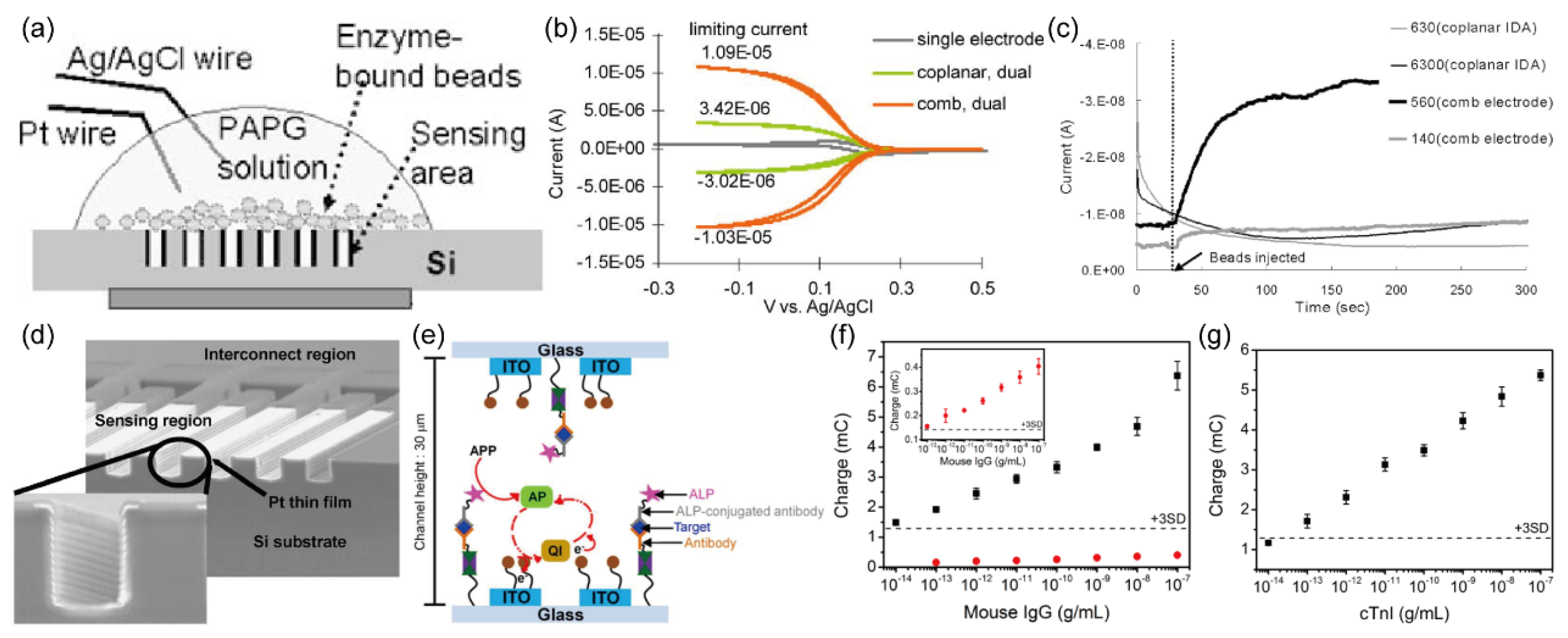
All the aforementioned investigations have primarily employed planar IDA electrodes, focusing on the influence of microband width and the gap between them on sensitivity, while overlooking the height of the microbands. To further enhance the sensitivity of immune detection and comprehensively explore the impact of height on redox cycling, Sang Kyung Kim and colleagues
29 conducted a study involving the fabrication of comb-shaped IDA with specific heights. In
Figure 15. (d), the SEM image of these 3D comb-shaped IDA shows prominent microband heights, which are anticipated to significantly enhance the redox cycling process between the generator and collector electrodes. A comparative analysis of cyclic voltammetry measurements in potassium ferricyanide solution, involving both coplanar and 3D comb-shaped IDA, is presented in
Figure 15. (b). Evidently, the 3D comb-shaped IDA demonstrate an amplified current response under identical conditions.
Figure 15. (a) shows the experimental setup, highlighting the use of magnetic beads with a diameter of 2.8 μm, which is slightly larger than the gap (2.4 μm), facilitating the secure placement of most beads on the surface of the comb-shaped IDA electrodes. These beads serve as solid supports for enzymatic reactions, enhancing analyte concentration in the solution and facilitating the efficient transfer of enzymatic reaction products to the electrode surface, thereby streamlining signal detection. The intimate contact between the beads and the IDA surface further promotes the transfer of PAP reaction products from enzymatic reactions to the IDA surface for subsequent redox reactions. Refer to
Figure 14. (a) for an elucidation of the principles governing the PAPG enzymatic reaction and PAP redox reaction. Following bead injection, the temporal evolution of current changes for the two types of IDA electrodes is depicted in
Figure 15. (c). Based on the data presented therein, the detection limit for β-galactosidase was determined to be 70 amol. Notably, the utilization of comb-shaped IDA electrodes enabled the completion of detection in less than 1 minute, as clearly demonstrated in
Figure 15. (c).
To further augment the electrochemical redox cycling process and enhance the sensitivity of immune sensors, Donghoon Han and colleagues
73 devised a novel approach involving the combination of two sets of comb-shaped IDA electrodes to form a face-to-face three-dimensional (3D) IDA electrode configuration, as shown in
Figure 15. (e). This distinctive face-to-face 3D IDA electrode is fabricated using indium tin oxide (ITO) material, with microband widths of 5 um and inter-microband gaps of 10 μm. The research team employed a double-sided adhesive film, employing a precision blade to create a slender slit, which was subsequently employed to connect the two comb-shaped IDA, effectively establishing a microfluidic channel. Within this channel, carefully pretreated samples, such as mouse IgG, were introduced to initiate the desired reactions. The 3D immune sensor platform was constructed, integrating ALP as an enzyme label, electroactive ferrocene as an electron mediator, and PAPP as the enzyme substrate, as illustrated in
Figure 15. (e). The enzymatic reaction involving PAPP and the ensuing redox reaction of PAP are shown in
Figure 14. (a). In
Figure 15. (f), (g) the response signals generated from various concentrations of mouse IgG and cardiac troponin I (cTnI) are presented. Notably, in
Figure 15. (f), the face-to-face 3D IDA configuration, owing to its efficient redox cycling of electroactive species, exhibits a remarkable approximately 100-fold enhancement in limiting current. The detection limit for mouse IgG was notably reduced to 10 fg/mL (indicated by black squares in
Figure 15. (f), a significant improvement compared to the 2D IDA setup, which featured a detection limit of 100 fg/mL (red circles and inset in
Figure 15. (f). Furthermore, as demonstrated in
Figure 15. (g), the face-to-face 3D IDA immunosensor introduced by the authors has been successfully applied in clinical analyses, showcasing its efficacy in the sensitive detection of cTnI in human serum, achieving an impressive detection limit of 100 fg/mL.
Taking into account the comprehensive exploration of the studies mentioned earlier, it becomes evident that IDA demonstrates a profound capacity to substantially enhance the sensitivity and response signal of sensors when integrated into immune sensing applications, primarily attributable to their distinctive redox cycling attributes. These immune sensors, harnessing the redox cycling prowess of IDA, hold promise for advancing medical diagnosis and disease prevention.
3.1.3. Ion detection
In light of the rapid advancement of industrial activities, environmental contamination has emerged as an exceedingly pressing concern. For example, the eutrophication of water resources caused by large amounts of nitrogen-based compounds in industrial wastewater has been considered as a common environmental problem.80 This concern is chiefly assessed through the determination of total nitrogen content (TN), encompassing both inorganic and organic fixed nitrogen species, within water bodies. Notably, the pivotal phase in gauging TN levels in water entails the quantification of nitrate concentration, a methodology frequently employed due to its user-friendly operation and rapid responsiveness.81
Jing Fang Hu and colleagues
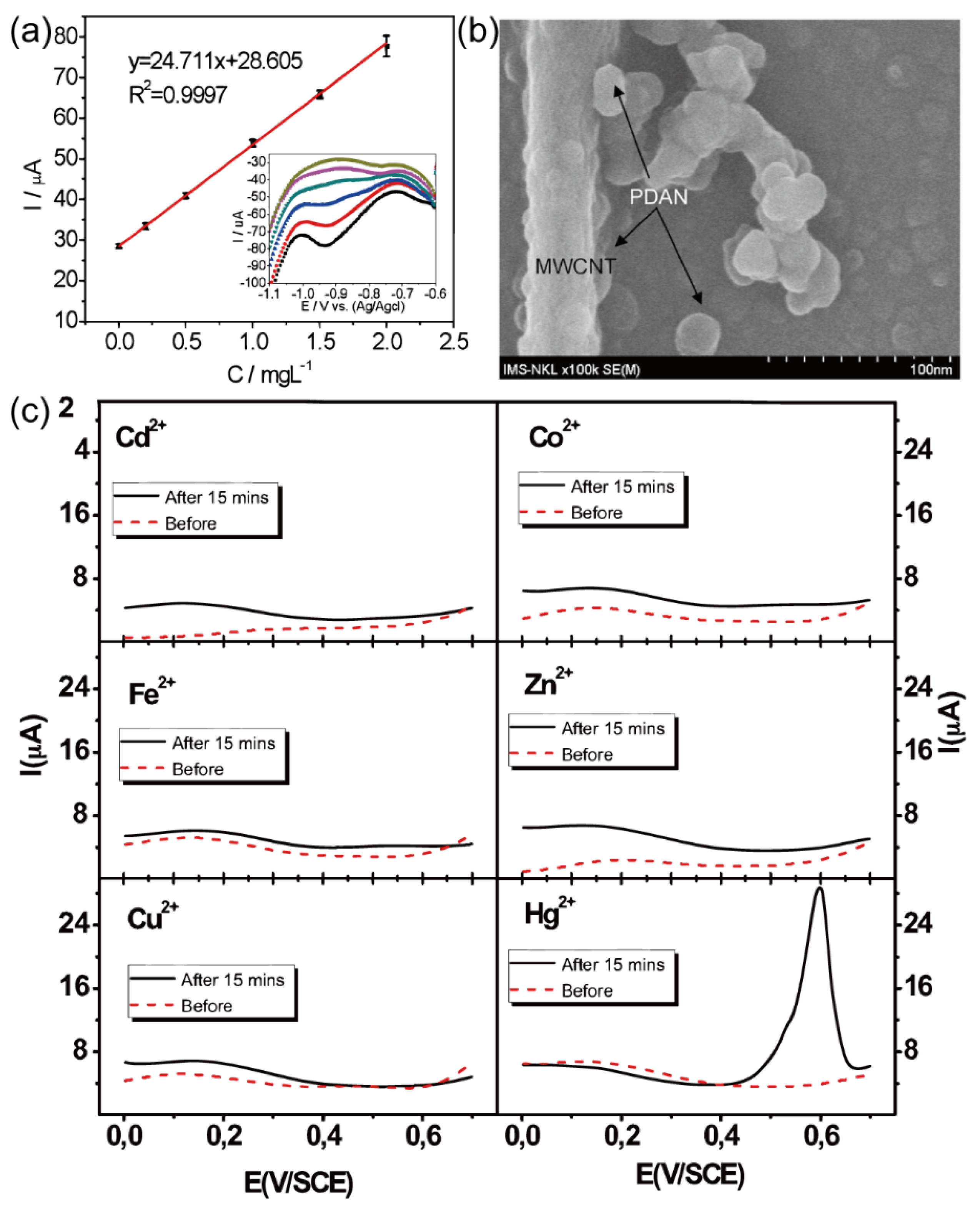
50 introduced an innovative approach for the detection of TN employing Au IDA electrodes modified with a palladium-based bimetallic catalyst, specifically a silver/palladium bimetallic composite (referred to as Ag/Pd-nanodendrites-modified Au IDA). The Au IDA electrodes are of 10 μm in width, 50 μm in gap, and 1500 μm in length. The 3D Ag/Pd nanodendrites were synthesized by electrodepositing silver (Ag) and palladium (Pd) onto the Au IDA electrodes. Remarkably, the 3D Ag/Pd-nanodendrites-modified Au IDA electrodes demonstrated the capability to efficiently quantify TN without necessitating pH adjustment, offering substantial potential for the development of cost-effective and portable instrumentation for TN detection. The detection process comprised several steps: Initial pretreatment of the water sample involved the use of potassium persulfate (K
2S
2O
8) and sodium hydroxide (NaOH), followed by heating at 120 °C for 30 minutes to ensure complete conversion of TN to nitrate. Subsequently, a 10 mL aliquot of the prepared solution was introduced into the electrochemical cell, where the nitrate content was determined through square-wave voltammetry under specific conditions (potential range: -0.7 to -1.2 V vs. Ag/AgCl, scanning frequency: 25 Hz). The relationship between the obtained cathodic current and the nitrate concentration is illustrated in
Figure 16. (a). Notably, this method exhibited a commendable detection limit of 0.1 mg/L, thereby eliminating the need for pH adjustment during TN determination using the described sensing microelectrode.
Furthermore, aside from the concern over TN, there exists a substantial need for monitoring heavy metal ions, particularly mercury ions (Hg
2+), due to their potential causing of severe environmental issues.
82 Traditional optical analysis methods and detection approaches employing organic fluorophores exhibit limitations characterized by inadequate stability, low sensitivity, and suboptimal selectivity. Therefore, Dzung Tuan Nguyen and colleagues
28 have conceived an electrochemical detection device for mercury ions based on the IDA structure, employing square wave voltammetry (SWV). This innovative approach utilizes the remarkable sensitivity of polydiaminonaphthalene (PDAN), a multifunctional polymer, toward heavy metal ions. However, PDAN's inherent drawback is its limited specific surface area, impeding the efficient collection and retrieval of metal ions from aqueous solutions. To address this, the research team integrated PDAN with carbon nanotubes (CNT) to fabricate a PDAN/CNT-based IDA electrode for the electrochemical detection of mercury ions. The fabrication process involved immersing the prepared IDA electrode in a solution containing 0.1 M HClO
4, 10
-3 M DAN, and 0.01% functionalized carbon nanotubes for electropolymerization, yielding the PDAN/CNT-modified IDA electrode, as described in
Figure 16. (b). Subsequently, the modified IDA electrode was immersed in the sample solution at the open circuit potential (E=+ 0.35 V vs. saturated calomel electrode, SCE) for 15 minutes. Following this pretreatment, the detection phase was initiated. Upon thorough cleansing of the electrode to remove metal ion salts with deionized water and ethanol, square wave voltammetry (SWVs) was conducted in 0.1 M HClO
4 solution under specific conditions (potential range: 0-0.7 V, frequency: 125 Hz, step: 8 mV, amplitude: 25 mV). The SWV curve is visually represented in
Figure 16. (c), demonstrating the electrode's response to Hg
2+ compared to other metal ions, thereby enabling selective detection of Hg
2+ even in the presence of competing ions. The authors of this study postulate that the high redox potential (Hg
2+/Hg
22+=+0.67 V vs. SCE) associated with Hg
2+ plays a critical role in its discrimination from other ions during detection.
3.1.4. Others
In addition to the biological detection mentioned above, the redox cycling property of IDA has also been used to conduct other studies, such as the determination of diffusion coefficient25, 26, 83 and the exploration of electroluminescence mechanism.84
B. J. Feldman and Royce W. Murray25 conducted an investigation into the diffusion coefficient of Prussian blue employing IDA electrodes. The experimental procedure involved initially depositing a Prussian blue film onto Pt IDA electrodes with specific dimensions (width: 3.5 µm, gap: 2.5 µm, height: 0.32 µm). The electroactive material under examination was Prussian blue, and the researchers assessed the limiting current associated with the reversible Fe (III/II) → Fe (II/II) reduction process (occurring at 0.2 V vs. saturated silver-silver chloride electrode, SSCE) in a KNO3 electrolyte. They successfully ascertained the diffusion coefficient of Prussian blue by employing a derived calculation formula , where various parameters were considered, including the center-to-center electrode spacing (p, 6 µm), the number of finger electrodes (N, 41), the dimension of a film-filled gap (d), and the charge collected (Q).
In a distinct investigation by Manfred Paeschke et al.,83 the electrochemical behavior of cytochrome c was explored using Au IDA electrodes (width: 2.9 µm, gap: 1.1 µm, number of microbands: 70) that were modified with 4,4'-dithiodipyridine and N-acetyl cysteine. Unlike the approach employed by B. J. Feldman and Royce W. Murray, this study focused more on the time required for the collector electrode to reach a steady-state current (designated as tmax). The theoretical calculation of the diffusion coefficient was derived from this parameter, expressed as , where D signifies the diffusion coefficient, θ represents a numerical factor specific to the system (with a value of 25.6), and Wgap denotes the gap width (1.1 µm). To obtain dynamic redox recycling measurements, the researchers conducted differential pulse voltammetry, and the resulting tmax was measured to be 370 milliseconds. Consequently, the calculated diffusion coefficient was determined to be 8.37 x 10^-7 cm^2 s^-1. F. Liu et al.85 presented the method for experimentally determining the diffusion coefficient of ions with IDA electrodes
Additionally, Alexander B. Nepomnyashchii and colleagues
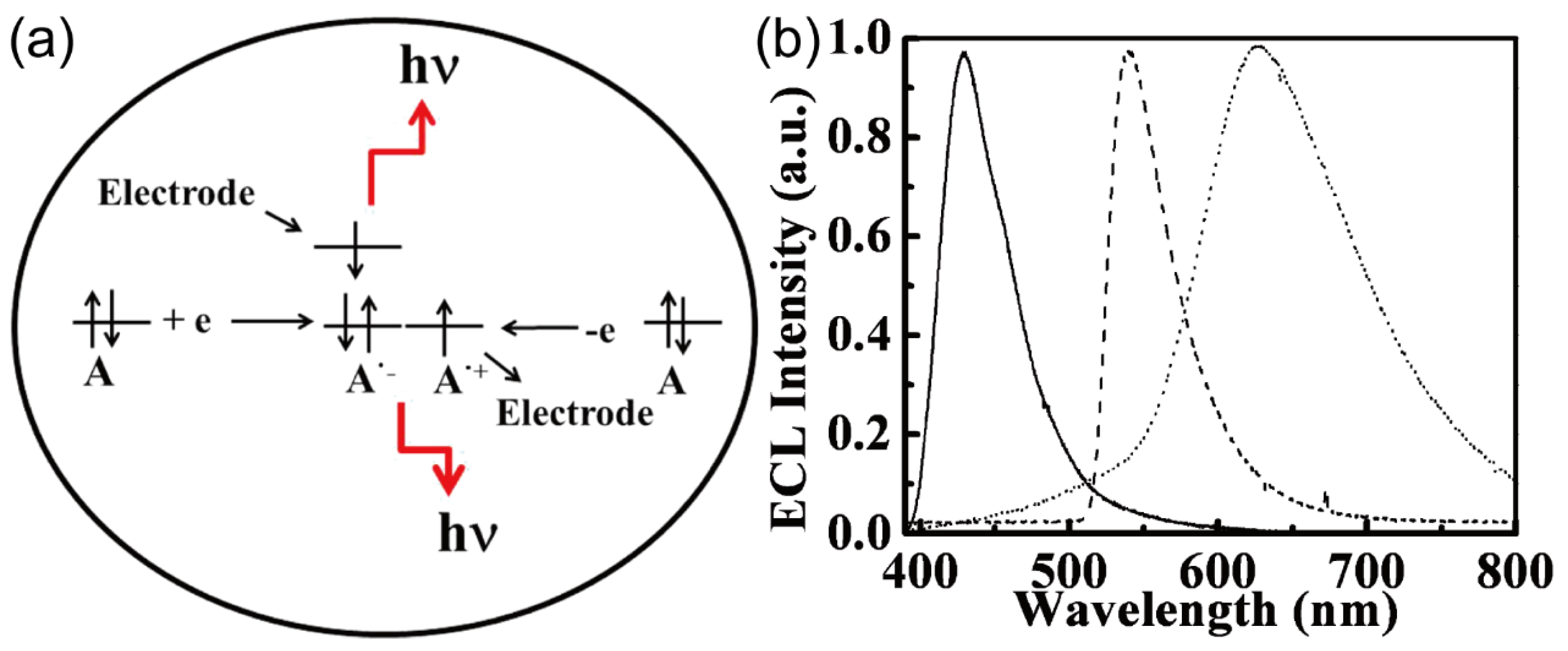
84 conducted investigations employing Pt IDA electrodes (width: 10 µm, gap: 5 µm, length: 2 mm) to generate high-intensity electrogenerated chemiluminescence (ECL) and explore the associated mechanisms. ECL is a phenomenon involving the electrochemical generation of light via highly exothermic reactions between reducing and oxidizing species present in a solution (
Figure 17. (a)). In an ingenious approach, the authors harnessed the capabilities of IDA electrodes to achieve a state of steady-state electrogenerated ECL with both annihilation and coreactant modes. Most annihilation-based ECL processes typically rely on potential step or potential sweep experiments to facilitate the generation of oxidized and reduced forms of molecules. However, the temporal delay involved in generating these oxidized or reduced molecules tends to limit the achievable ECL intensity. To eliminate this limitation, the authors employed IDA electrodes to simultaneously generate the oxidized and reduced forms of molecules on the two working electrodes of IDA, avoiding the time lag. This strategic approach resulted in a remarkable increase in ECL light output, achieving an astonishing 100-fold enhancement in comparison to that obtained with conventional planar electrodes possessing a comparable surface area. Detailed electrochemiluminescence spectra for the three substances of interest are thoughtfully presented in
Figure 17. (b)
3.2. Application based on IDA electrodes resistance and impedance variation
3.2.1. Gas sensing
Gas sensors are vital for monitoring environmental conditions, especially toxic gases like carbon monoxide (CO) and ammonia (NH
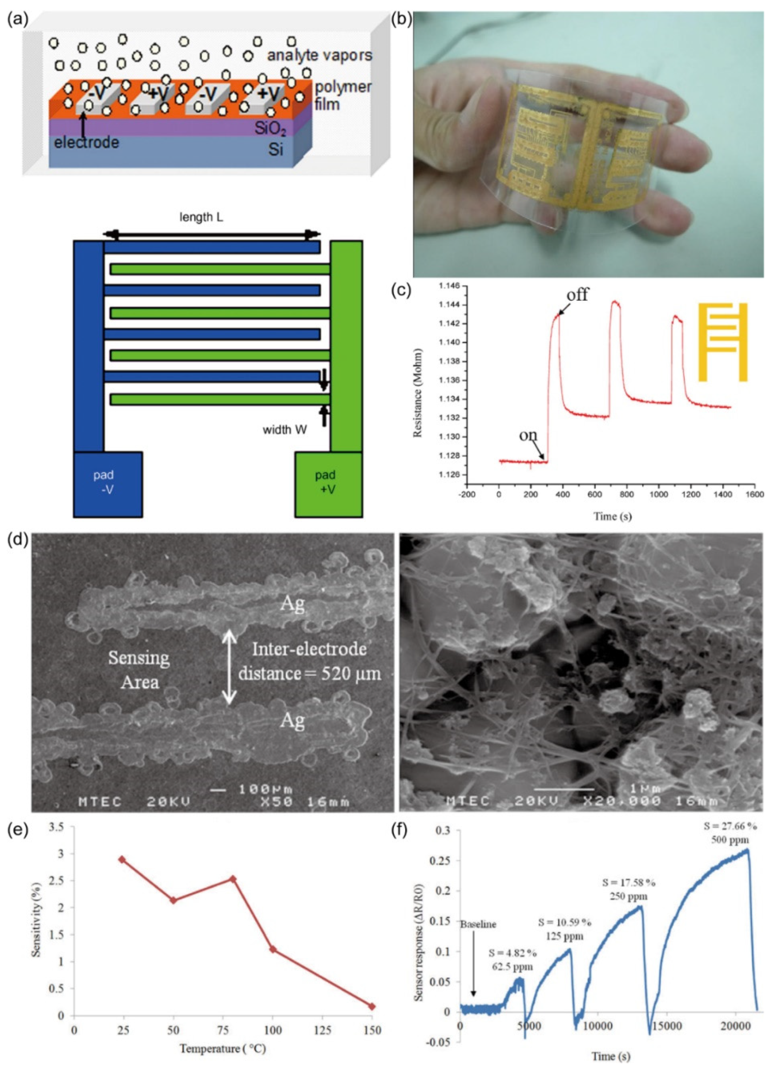
3) that pose health risks. Resistive gas sensors operate by altering the resistance of gas-sensitive materials in response to gas molecules. Consider an IDA-structured gas sensor as an example. When analyte vapors diffuse onto the IDA electrode surface, it modifies the sensing layers, so as to be detected, as illustrated in
Figure 18. (a). Gas sensors employing gas-sensitive materials on IDA structures offer simplicity and suitability for mass production compared to other sensor types.
86 This is essential for effective gas monitoring.
D.M. Liu et al.
87 developed a CO gas sensor utilizing a polypyrrole-film-modified IDA electrode. Sensor performance is assessed using sensitivity (S), calculated as the percentage change in resistance: S = 100 (ΔR/R
0), R
0 is the resistance at zero CO concentration. The sensor exhibited a maximum sensitivity of 6.5% at 500 ppm CO concentration. Chun-Chieh Tseng et al.
40 fabricated a carbon dioxide (CO
2) sensor using a poly(3,4-ethylenedioxythiophene)–poly(styrene sulfonate) (PEDOT-PSS) membrane-modified Au IDA via inkjet printing and electroless plating. The sensor, positioned on a flexible PET substrate (
Figure 18. (b)), exhibited an increase in resistance when exposed to 100 ppm CO
2 concentration, as depicted in
Figure 18. (c). The sensor demonstrated a sensitivity of 7 × 10
−3%/ppm for CO
2, surpassing the sensitivity of polypyrrole film-modified CO
2 sensors (6 × 10
−4%/ppm)
88 and exhibiting faster response and recovery times.
To enhance the sensitivity of a gas sensor, Pattamon Teerapanich et al.
20 devised a NH
3 sensor by modifying a Ag IDA with single-walled carbon nanotubes (SWCNTs), offering an economical and straightforward NH
3 detection approach. The fabrication process involved printing the IDA structure on an alumina substrate using Ag nanoparticle inks via inkjet printing, followed by annealing at 300 °C. An electroplated nickel layer was added to enhance electrode conductivity and corrosion resistance. Subsequently, a 10 μL suspension of SWCNTs was drop-deposited onto the heated IDA sensing area at 80°C, forming SWCNT networks across the electrode fingers. Alumina, as the substrate, presented advantages such as lower cost, excellent dielectric properties, thermal stability, and porosity, facilitating ink adhesion during inkjet printing and promoting SWCNT adhesion. The significant specific surface area of SWCNTs contributed to improved gas adsorption, thereby enhancing sensor sensitivity.
Figure 18. (d) displays a SEM image of SWCNTs on the Ag IDA sensing region. NH
3, acting as an electron donor on the p-type CNT surface, led to NH
3 adsorption reducing hole carrier concentrations within the CNTs, consequently increasing the electrical resistance of the CNT film. This resistance change was monitored by measuring the alteration in resistance between the two IDA electrodes. Optimal sensor operation was achieved at room temperature (
Figure 18. (e)), yielding a sensitivity of 2.9%. The sensor demonstrated varying degrees of sensitivity to different NH
3 concentrations (
Figure 18. (f)), with the highest sensitivity recorded at 27.66% for 500 ppm NH
3. The sensor's detection limit for NH
3 was approximately 3 ppm at room temperature.
3.2.2. pressure sensing
Beyond gas sensing, flexible sensors can also monitor human movements involving pressing, bending, and stretching. The intricate nature of deformations and stimuli variations poses a challenge for accurately discerning external triggers in flexible sensors. Addressing this issue, Xin Li et al.
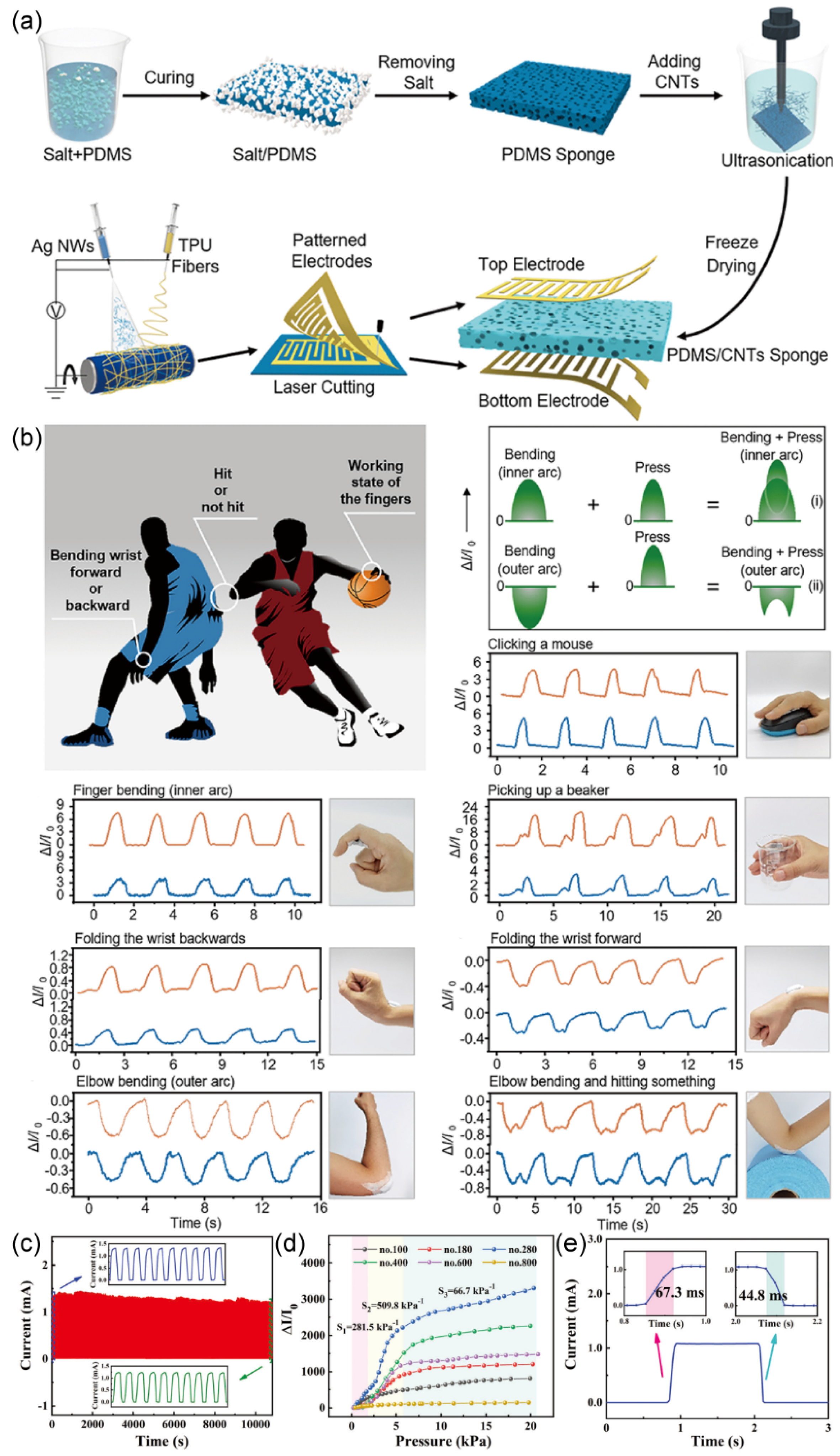
89 introduced a Flexible Dual-Interdigital-Electrode Sensor (FDES). The FDES comprises a pressure-sensitive porous conductive sponge and two IDA electrodes. When exposed to external stimuli, such as compression, positive or negative bending, or stretching along the X or Y directions, the resistance of the sponge interlayer undergoes changes. This, in turn, allows for precise detection of current alterations in the IDA, facilitating the sensing and characterization of bodily movements. The fabrication process of the FDES is elucidated in
Figure 19. (a). Initially, pressure-sensitive porous conductive sponges were constructed by depositing Carbon Nanotubes (CNTs) onto elastic polydimethylsiloxane (PDMS) sponges. Subsequently, two IDA, created via laser etching of conductive films, were affixed to both sides of the PDMS/CNTs sponge, serving as the top and bottom electrodes. The FDES was subjected to various human movement scenarios, including mouse clicking, finger bending, beaker holding, wrist folding backward, wrist folding forward, arm bending, arm bending, and object impact. These scenarios demonstrated the FDES's capability to identify and distinguish specific human movements, as illustrated in
Figure 19. (b).
Furthermore, Mei Yang et al.
90 employed an economical spray deposition method to fabricate flexible pressure sensors based on a composite of MXene, polyurethane (PU), and IDA Electrodes. The research team subjected the sensor to a series of performance assessments and the sensor exhibited good stability, with its performance remaining largely unaltered after undergoing 10,000 pressure cycles at 14.2 kPa (
Figure 19. (c)). Additionally, the sensor displayed rapid response (67.3 ms) and short recovery times (44.8 ms) (
Figure 19. (e)), alongside high sensitivity (281.5 kPa
-1 at 0.30-2.00 kPa, 509.8 kPa
-1 at 2.00-5.70 kPa, 66.7 kPa
-1 at 5.70-20.70 kPa) (
Figure 19. (d)). Also, utilizing the presence of hydrogen bonds within the PU component, the sensor exhibited self-healing capabilities. Consequently, this flexible pressure sensor holds promise for applications in electronic skin, human motion detection, and related fields.
3.2.3. Humility sensing
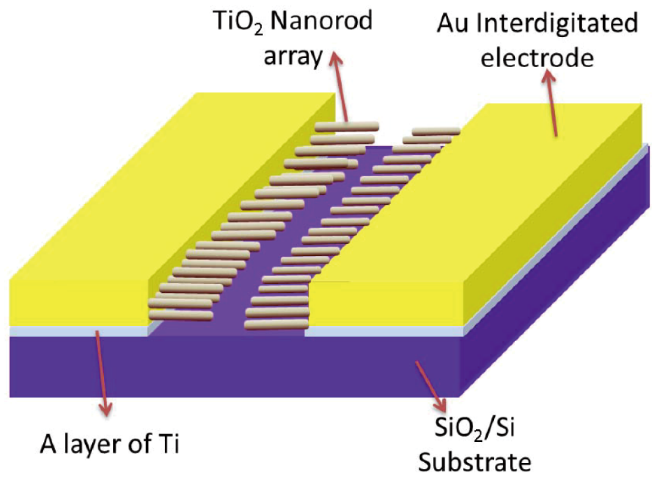
Humidity sensing holds significance in various applications such as greenhouse cultivation, pharmaceutical and food storage. The IDA structure has also found application in humidity sensing. Commonly employed humidity sensors encompass resistance, capacitance, and thermal types. For instance, Xuan Zhao et al.
74 fabricated an Au-IDA utilizing photolithography techniques on a SiO
2/Si substrate, as depicted in
Figure 20. This sensor featured hydrothermally grown TiO
2 nanorods situated between the IDA digits. TiO
2 nanorods exhibit high sensitivity to humidity variations and possess the capacity to adsorb water molecules, leading to a reduction in impedance between the IDA digits. Utilizing the IDA's porous structure and substantial surface area, the sensor can efficiently capture water molecules even under low humidity conditions, enabling precise environmental humidity detection. Notably, this sensor demonstrated a broad humidity detection range spanning from 11.3%RH to 97.3%RH.
3.2.4. Biological sensing
The application of IDA in biochemical detection, utilizing its unique redox cycling property, has been elaborated in
Section 3.1. An alternative approach to biochemical detection involves monitoring changes in the impedance of IDA electrodes. Zhiwei Zou et al.
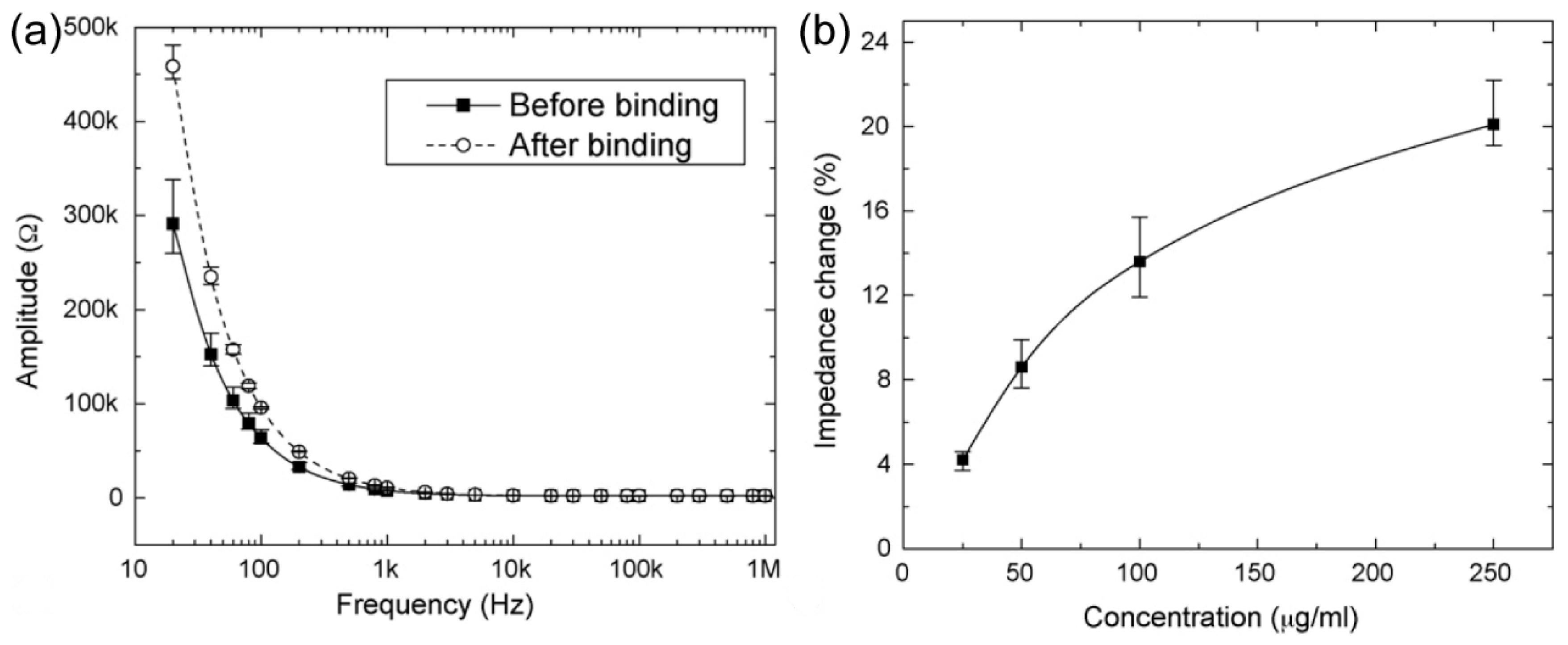
44 devised nano-sized Au IDA (width 200 nm, gap 500 nm, length 100 µm) on a cycloolefin copolymer (COC) substrate utilizing e-beam lithography techniques to create a biosensor. In this biosensor, the binding of proteins (specifically, mouse IgG) to the IDA electrode surface results in the formation of a newly charged layer on the electrode surface. This phenomenon introduces modifications to the sensor's equivalent circuit, effectively acting as a series capacitor.
Figure 21. (a) illustrates the impedance alterations, which predominantly occur within the low-frequency range (20 Hz - 1 kHz) following protein binding to the electrode surface. Subsequently, impedance variations were assessed at 100 Hz for varying concentrations of mouse anti-rabbit IgG, as demonstrated in
Figure 21. (b) The authors of this study propose that this sensor exhibits significant potential for application in enzyme-free bioanalysis.
3.3. Application based on IDA electrodes capacitance variation
In addition to the utilization of impedance variations, Yalei Zhao et al.
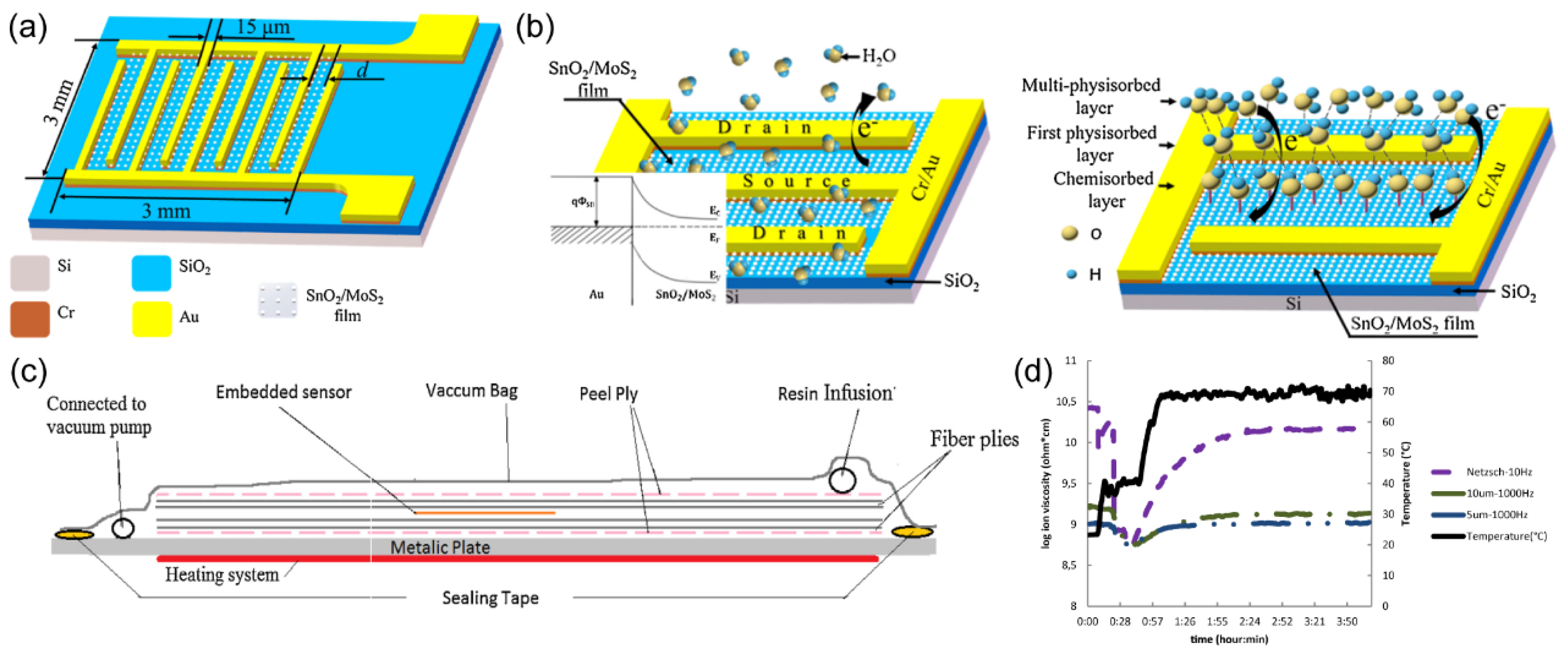
91 employ changes in capacitance of ion-selective electrode (IDA) setups for humidity sensing. The study underscores the critical influence of IDA size on the underlying detection mechanism, which needs further investigation. Zhao's work encompasses the fabrication of a humidity-sensitive layer-coated Au IDA, a visual representation of which is provided in
Figure 22. (a). The sensitive layer, comprised of SnO
2/MoS
2, was prepared via a two-step hydrothermal synthesis method. The authors believe that the sensor can be sensed in two ways. For sensors with a small gap, electrons play a major role in charge transfer, and the sensing mechanism is based on the interaction of water molecules with SnO
2/MoS
2. Adsorbed water molecules trap electrons and act as p-type doping on the sensing film, which will reduce the charge density and lower the capacitance of the sensor. For the sensor with large gap, proton hopping through water layers plays a dominant role and the capacitance of the sensor is related to the conductivity of the proton. High humidity generated a liquid-like water layer, protons hopping transport carried out, and led to the increase of capacitance. The schematic diagram of sensing principle is shown in
Figure 22. (b).
Furthermore, Maryam Kahali Moghaddam and colleagues
92 utilize the alteration in capacitance of ion-selective electrode (IDA) configurations to monitor the resin curing process—an innovative approach. Their research involved the utilization of polyimide as the substrate material and tantalum oxide film as the electrode layer, followed by the fabrication of the IDA structure via lithographic techniques, culminating in the successful construction of the sensor apparatus. Subsequently, this sensor was integrated into a rectangular pre-fabricated housing situated atop a layer of glass fiber (
Figure 22. (c)). The dynamic progression of the resin curing process was monitored in real-time by means of dielectric analysis (DEA), focusing on the modulation of ionic viscosity. As the resin traversed the heated glass fiber laminate, it experienced a rise in temperature, leading to a straightforward softening reaction and a concomitant reduction in ionic viscosity. This relationship between ionic viscosity and temperature is shown in
Figure 22. (d). The vigilance over the resin curing process affords valuable insights into the optimal process conditions conducive to the production of high-quality complex composite materials, thereby enhancing cost efficiency within this domain.
3.4. Devices based on the special structure of IDA
Beyond its utility in electrochemical sensing, IDA, with typical dimensions of below 15 μm, possesses distinctive features that make it suitable for deployment in energy storage and conversion devices. While rechargeable energy storage devices hold important roles in portable electronic devices and emerging electric vehicles powered by new energy sources, capacitors, as a category of energy storage systems, stand out due to their high-power capabilities and inherent stability. Nonetheless, traditional capacitors have limitations in energy storage capacity, exacerbated by their bulky sandwich-like structures. To enhance the performance of energy storage devices, certain researchers have applied IDA configurations in capacitor design. Their findings suggest that IDA-based capacitors outperform their conventional counterparts, offering a promising avenue for improved energy storage systems.
3.4.1. Capacitors
To enhance the energy density of capacitors, Fangming Han and colleagues
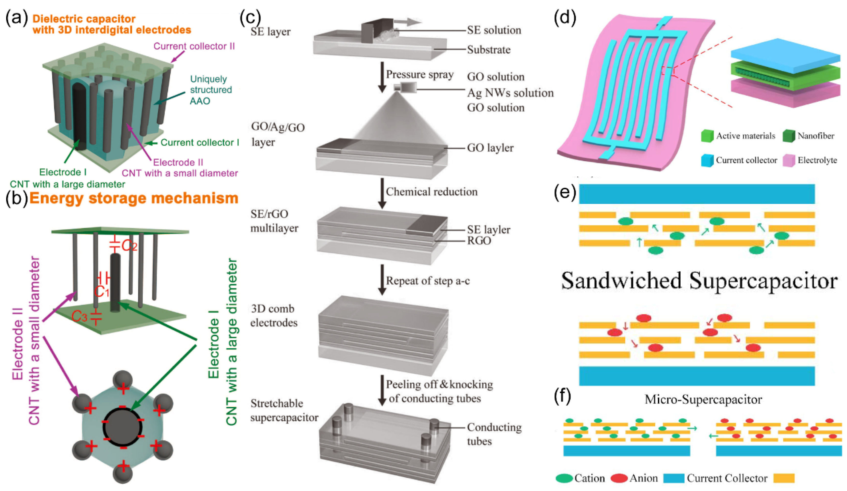
93 introduced a dielectric capacitor featuring 3D IDA electrodes. This 3D IDA capacitor shows several advantages including a high breakdown voltage, substantial capacitance, and an impressive energy density of up to 2 Wh/kg. The researcher approach involved the fabrication of a unique nanoporous anodized aluminum oxide (AAO) film, within which carbon nanotubes (CNTs) were strategically deposited to serve as electrodes, arranged in a cross configuration within the film's pores (
Figure 23. (a)). The storage mechanism of the 3D IDA capacitor is elucidated in
Figure 23. (b). The authors believed that the equivalent capacitance (C
total) is approximated as is
, where C
1 signifies the capacitance between adjacent CNTs on opposing electrodes, and C
2 and C
3 represent the capacitance between the arrays of CNT tips and the respective opposing electrodes.
Fengwang Li and colleagues
32 also engineered a supercapacitor featuring a 3D structure, employing reduced graphene oxide (rGO) as the primary material. Although rGO offers notable advantages like a high specific surface area and exceptional electrochemical performance, its volume capacitance in supercapacitors falls short of ideal standards. In response to this challenge, the research team introduced supercapacitors characterized by a 3D IDA structure, wherein each IDA electrode comprises a solid electrolyte film and an overlay of rGO film, as illustrated in
Figure 23. (c). Performance assessments revealed that the specific capacitance of the supercapacitor reached 121 F/g, while the volume capacitance achieved an impressive 28.3 F/cm
3 with a 1 µm-thick rGO film, surpassing the average commercial supercapacitor in this regard.
3D structures have proven to be instrumental in enhancing the performance of supercapacitors. Achieving smaller device sizes holds significant promise for expanding their practical utility in micropower systems. Yu Song and colleagues
31 engineered a Micro-Supercapacitor (MSC) featuring an IDA structure. Their design utilized a flexible substrate and ion reservoir composed of polyvinyl alcohol/phosphoric acid (PVA/H
3PO
4) gel electrolyte, carbon nanotubes (CNTs) as electrodes, and a gold film for current collection, as illustrated in
Figure 23. (d). The team employed a cost-effective laser etching process to obtain the IDA structure. As depicted in
Figure 23. (e), when compared to conventional supercapacitor architectures, the MSC with the IDA configuration maximizes the utilization of the active material surface, substantially shortening the pathway for electrolyte ion transport (
Figure 23. (f)). Consequently, it achieves superior capacitance and enhanced energy storage capabilities. This type of MSC exhibits promising potential for applications in microelectronic device power supply systems.
Haibo Hu and colleagues30 employed a combination of laser printing, vacuum-assisted deposition, and physical sputtering techniques to facilitate the creation of an IDA structure using MXenes on printing paper. This approach allowed for the assembly of multi-layered MXenes sheets in a coplanar fashion, forming a planar-symmetric Micro-Supercapacitor (MSC). Notably, the maximum area capacitance achieved by this MSC configuration exhibited a remarkable increase of at least 460% when compared to carbon-based MSCs.
In conclusion, the utilization of an IDA structure in the fabrication of MSCs has proven to be an effective approach to enhancing their energy storage capabilities. Employing laser printing for creating the essential IDA pattern simplifies the fabrication process and concurrently reduces production costs. This method serves as a valuable reference for the pragmatic advancement of high-performance micro-power supply systems.
3.4.2. Photodetector
Several research studies55, 94-96 have involved the fabrication of photodetectors employing IDA structures. Kang Liu and colleagues94 introduced a diamond UV detector characterized by a gold back contact on its rear surface and an IDA structure on its front surface (width: 160 μm, gap: 160 μm). The incorporation of a gold back contact serves to enhance the detector's response rate and detection efficiency. This improvement can be attributed to the gold back contact's role as the rear electrode, which facilitates the more efficient collection of UV-excited carriers, consequently augmenting the overall performance of the detector.
Wei Zhang and colleagues
95 fabricated UV photodetectors utilizing a MgZnO material with an IDA structure. Their investigation focused on assessing the impact of varying the number of interdigital electrode pairs on the device's performance. The research team initially employed RF magnetron sputtering to deposit a MgZnO thin film (280 nm thick) onto a quartz substrate. Subsequently, they applied a layer of Au thin film (122 nm thick) on top of the MgZnO thin film. The IDA structure was then created through lithographic techniques with width and gap of 5 μm each (
Figure 24). When subjected to UV irradiation at an intensity of 500 μW/cm
2, the photodetector with the greatest number of interdigital electrode pairs (N=25) exhibited consistent response stability and the most favorable overall performance.
Furthermore, aside from ultraviolet (UV) photodetectors, near-infrared (NIR) photodetectors featuring IDA structures can be created using different semiconductor and metal materials. A notable achievement in this domain was realized by A. I. Nusir et al.,55 who successfully fabricated a NIR photodetector employing GaAs as the substrate material. They applied a layer of titanium film and gold film to enable the formation of the IDA pattern, following established lithography procedures. Interestingly, Mengyao Zhang and colleagues96 introduced a method for IDA structures fabrication directly in solution, eliminating the need for lithography. They achieved this by combining the synthesis of gold nanoparticles (AuNPs), interfacial self-assembly, and plasma welding techniques. Subsequently, they prepared a CH3NH3PbI3 thin film on the IDA structure through vacuum deposition, spin coating, and annealing processes, thus creating a perovskite photodetector.
3.4.3. Nanogenerators
Nanogenerators (NGs) are an interesting research area in the field of energy harvesting, as they have the capability to convert insignificant mechanical energy present in the environment into electrical energy, which can be harnessed to power small-scale electronic devices. Notably, researchers have explored the integration of IDA structures into the fabrication processes of NGs, yielding promising outcomes. For instance, Jinzheng Gui et al.38 employed electrospinning techniques to create a layer of poly(vinylidene fluoride trifluoroethylene) [P(VDF-TrFE)] nanofibers film on an Au IDA substrate. Through a packaging process involving polydimethylsiloxane (PDMS) and a cylindrical mold, they fashioned a piezoelectric nanogenerator (PENG) featuring a cavity. Concurrently, Au-IDA structures (width: 18 μm, gap: 200 μm) were meticulously prepared on a polyimide substrate via photolithography and wet etching methods. In a parallel effort to improve the output performance of the PENG, Lingling Zhang et al.97 devised a 3D IDA configuration coupled with [P(VDF-TrFE)] nanofibers for their PENG design, incorporating a specified height dimension. This 3D IDA structure not only enhances the adaptability of the nanofibers in terms of shape but also amplifies the contact area between these nanofibers and the electrode, thereby augmenting the output voltage and current of the PENG.
4. Conclusion
As previously elucidated, the distinctive structural attributes of IDA electrodes, characterized by the presence of two interdigitated comb-like arrays with micron-scale dimensions, render them a compelling candidate for supplanting conventional two-working electrode configurations of RRDE.
IDA electrodes demonstrate the capacity for significantly heightened collection efficiency and signal-to-noise ratio, and functioned as a signal amplifier, primarily attributable to the intrinsic "feedback" effect. These attributes have facilitated their applications across diverse scientific domains, including but not limited to trace biomolecular detection, gas sensing applications, and enhancements in capacitance, among others.
Nonetheless, the relative underrepresentation of IDA electrodes versus. RRDE can be attributed predominantly to two factors:
1. Sample Modification: While both IDA and RRDE find utility in homogeneous and heterogeneous reactions, the latter often necessitates the deposition of samples onto the surface of the generator electrode. This operation is readily accomplished with RRDE but shows a considerable challenge for IDA electrodes due to their micron-scale dimensions. Consequently, the development of methodologies for effective sample loading onto micron-scale IDA electrodes emerges as a critical effect for advancing the electrochemical application of IDA electrodes.
2. Experiment Reproducibility: IDA electrodes are frequently considered as one-time-use electrodes due to the fragility of their patterns, rendering them unsuitable for polishing before and after experiments (electrochemical cleaning and wet cleaning can be taken). As a consequence, the reproducibility of experimental results using identical IDA electrodes is compromised. However, this limitation can be mitigated by repeating experiments with various fresh-made IDA electrodes and calibrating them with electrode surface area (the electrochemical active surface area of IDA electrodes can be obtained through electrochemical ways —an easily attainable parameter through electrochemical techniques).
The future development of IDA electrodes and their applications have huge potential, with numerous uncharted realms for exploration. Several considerations need high attention:
1. Exploit the intrinsic "redox cycling" property and the "feedback" effect of IDA electrodes. While IDA electrodes have found extensive application in biomolecular detection, gas sensing, pressure sensing, and related fields, primarily relying on changes in resistance between the two groups of IDA digits. Nevertheless, the distinctive electrochemical properties underpinning "redox cycling" and the "feedback" effect remain underutilized and underappreciated. The inherent high sensitivity inherent in IDA electrodes due to the "feedback" effect can be further harnessed for the detection of reaction intermediates, particularly those with short lifetimes or low concentrations.
2. The compact dimensions of IDA electrodes offer a promising way for the miniaturization of devices. In contrast to Rotating Ring Disk Electrodes (RRDE), IDA electrodes feature micron-level dimensions and demand fewer ancillary components, all while delivering superior performance. This characteristic makes them suitable for integration as critical components, as well as for field deployment as portable tools.
3. It is critical to acknowledge that various fabrication techniques yield IDA electrodes with distinct characteristics. Inkjet printing emerges as a cost-effective and highly efficient fabrication strategy. However, further refinements are necessary to enhance the precision and reliability of IDA fabrication via inkjet printing.
In summation, the development of IDA electrodes in both their fabrication and application is marked by immense promise, thanks to their unique electrochemical properties and microminiaturization potential. Continued exploration of their capabilities and the refinement of fabrication techniques stand as essential endeavors in realizing their full potential across a large variety of scientific disciplines.
Acknowledgments
This research was supported by the Natural Science Basic Research Program of Shaanxi (Program No. 2023-JC-YB-116), the State Key Laboratory of Multiphase Flow in Power Engineering, and the National Natural Science Foundation of China (No. 51702250).
References
- Jia, Z.; Yin, G.; Zhang, J. Rotating ring-disk electrode method. In Rotating electrode methods and oxygen reduction electrocatalysts; Elsevier, 2014; pp. 199–229. [Google Scholar]
- Liu, F.; Divan, R.; Parkinson, B. A. Fabrication of Carbon-Platinum Interdigitated Array Electrodes and Their Application for Investigating Homogeneous Hydrogen Evolution Catalysis. Journal of The Electrochemical Society 2015, 162, H645–H650. [Google Scholar] [CrossRef]
- Niwa, O.; Tabei, H.; Solomon, B. P.; Xie, F.; Kissinger, P. T. Improved detection limit for catecholamines using liquid chromatography-electrochemistry with a carbon interdigitated array microelectrode. Journal of Chromatography B: Biomedical Sciences and Applications 1995, 670, 21–28. [Google Scholar] [CrossRef]
- Niwa, O.; Morita, M.; Tabei, H. Electrochemical behavior of reversible redox species at interdigitated array electrodes with different geometries: consideration of redox cycling and collection efficiency. Analytical Chemistry 1990, 62, 447–452. [Google Scholar] [CrossRef]
- Fiaccabrino, G.; Tang, X.-M.; Skinner, N.; De Rooij, N.; Koudelka-Hep, M. Interdigitated microelectrode arrays based on sputtered carbon thin-films. Sensors and Actuators B: Chemical 1996, 35, 247–254. [Google Scholar] [CrossRef]
- Odijk, M.; Olthuis, W.; Dam, V. e. A. e. T.; van den Berg, A. Simulation of Redox-Cycling Phenomena at Interdigitated Array (IDA) Electrodes: Amplification and Selectivity. Electroanalysis: An International Journal Devoted to Fundamental and Practical Aspects of Electroanalysis 2008, 20, 463–468. [Google Scholar] [CrossRef]
- Liu, F.; Kolesov, G.; Parkinson, B. A. Preparation, applications, and digital simulation of carbon interdigitated array electrodes. Analytical chemistry 2014, 86, 7391–7398. [Google Scholar] [CrossRef] [PubMed]
- Kamath, R. R.; Madou, M. J. Three-dimensional carbon interdigitated electrode arrays for redox-amplification. Analytical chemistry 2014, 86, 2963–2971. [Google Scholar] [CrossRef]
- Heo, J.; Shim, D.; Teixidor, G. T.; Oh, S.; Madou, M.; Shin, H. Carbon interdigitated array nanoelectrodes for electrochemical applications. Journal of the Electrochemical Society 2011, 158, J76. [Google Scholar] [CrossRef]
- Polonsky, J.; Rievaj, M.; Bustin, D. Interdigitated Array Electrode: A Sensor for Trace Electroanalysis. Chemical Analysis 1997, 42, 445–450. [Google Scholar]
- Hayashi, K.; Takahashi, J.-i.; Horiuchi, T.; Iwasaki, Y.; Haga, T. Development of nanoscale interdigitated array electrode as electrochemical sensor platform for highly sensitive detection of biomolecules. Journal of The Electrochemical Society 2008, 155, J240. [Google Scholar] [CrossRef]
- Kostecki, R.; Song, X.; Kinoshita, K. Electrochemical analysis of carbon interdigitated microelectrodes. Electrochemical and solid-state letters 1999, 2, 465. [Google Scholar] [CrossRef]
- Morita, M.; Hayashi, K.; Horiuchi, T.; Shibano, S.; Yamamoto, K.; Aoki, K. J. Enhancement of redox cycling currents at interdigitated electrodes with elevated fingers. Journal of The Electrochemical Society 2014, 161, H178. [Google Scholar] [CrossRef]
- Lee, S. J.; Pyun, S. I.; Lee, S. K.; Kang, S. J. L. Fundamentals of rotating disc and ring–disc electrode techniques and their applications to study of the oxygen reduction mechanism at Pt/C electrode for fuel cells. Israel Journal of Chemistry 2008, 48, 215–228. [Google Scholar] [CrossRef]
- Kulandainathan, M. A.; Kulangiappar, K.; Raju, T.; Muthukumaran, A. Cyclic voltammetry and RRDE studies on the electrochemical behavior of azetidinone ester. Portugaliae Electrochimica Acta 2005, 23, 355. [Google Scholar] [CrossRef]
- Costas, A.; Florica, C.; Preda, N.; Besleaga, C.; Kuncser, A.; Enculescu, I. Self-connected CuO–ZnO radial core–shell heterojunction nanowire arrays grown on interdigitated electrodes for visible-light photodetectors. Scientific Reports 2022, 12, 6834. [Google Scholar] [CrossRef] [PubMed]
- Lee, S. H.; Lee, J. H.; Park, C.; Kwak, M. K. Roll-type photolithography for continuous fabrication of narrow bus wires. Journal of Micromechanics and Microengineering 2016, 26, 115008. [Google Scholar] [CrossRef]
- Bidoki, S.; Lewis, D.; Clark, M.; Vakorov, A.; Millner, P.; McGorman, D. Ink-jet fabrication of electronic components. Journal of Micromechanics and Microengineering 2007, 17, 967. [Google Scholar] [CrossRef]
- Lee, J.-H.; Hwang, H.-J.; Kim, J.-H.; Hwang, K.-T.; Han, K.-S. Ceramic ink-jet printing on glass substrate using oleophobic surface treatment. Journal of the Korean Ceramic Society 2016, 53, 75–80. [Google Scholar] [CrossRef]
- Teerapanich, P.; Myint, M. T. Z.; Joseph, C. M.; Hornyak, G. L.; Dutta, J. Development and improvement of carbon nanotube-based ammonia gas sensors using ink-jet printed interdigitated electrodes. IEEE Transactions on Nanotechnology 2013, 12, 255–262. [Google Scholar] [CrossRef]
- Gittard, S. D.; Narayan, R. J. Laser direct writing of micro-and nano-scale medical devices. Expert review of medical devices 2010, 7, 343–356. [Google Scholar] [CrossRef]
- Kerbs, A.; Mueller, P.; Kaupp, M.; Ahmed, I.; Quick, A. S.; Abt, D.; Wegener, M.; Niemeyer, C. M.; Barner-Kowollik, C.; Fruk, L. Photo-Induced Click Chemistry for DNA Surface Structuring by Direct Laser Writing. Chemistry–A European Journal 2017, 23, 4990–4994. [Google Scholar] [CrossRef]
- Watanabe, A.; Cai, J. On demand process based on laser direct writing and the sensor application. Journal of Photopolymer Science and Technology 2017, 30, 341–343. [Google Scholar] [CrossRef]
- Daniel, D.; Gutz, I. G. Microfluidic cells with interdigitated array gold electrodes: Fabrication and electrochemical characterization. Talanta 2005, 68, 429–436. [Google Scholar] [CrossRef] [PubMed]
- Feldman, B.; Murray, R. W. Measurement of electron diffusion coefficients through Prussian Blue electroactive films electrodeposited on interdigitated array platinum electrodes. Analytical Chemistry 1986, 58, 2844–2847. [Google Scholar] [CrossRef]
- Nishihara, H.; Dalton, F.; Murray, R. W. Interdigitated array electrode diffusion measurements in donor/acceptor solutions in polyether electrolyte solvents. Analytical Chemistry 1991, 63, 2955–2960. [Google Scholar] [CrossRef]
- Niwa, O.; Xu, Y.; Halsall, H. B.; Heineman, W. R. Small-volume voltammetric detection of 4-aminophenol with interdigitated array electrodes and its application to electrochemical enzyme immunoassay. Analytical chemistry 1993, 65, 1559–1563. [Google Scholar] [CrossRef]
- Nguyen, D. T.; Dai Tran, L.; Le Nguyen, H.; Nguyen, B. H.; Van Hieu, N. Modified interdigitated arrays by novel poly (1, 8-diaminonaphthalene)/carbon nanotubes composite for selective detection of mercury (II). Talanta 2011, 85, 2445–2450. [Google Scholar] [CrossRef]
- Kim, S. K.; Hesketh, P. J.; Li, C.; Thomas, J. H.; Halsall, H. B.; Heineman, W. R. Fabrication of comb interdigitated electrodes array (IDA) for a microbead-based electrochemical assay system. Biosensors and Bioelectronics 2004, 20, 887–894. [Google Scholar] [CrossRef]
- Hu, H.; Hua, T. An easily manipulated protocol for patterning of MXenes on paper for planar micro-supercapacitors. Journal of materials chemistry A 2017, 5, 19639–19648. [Google Scholar] [CrossRef]
- Song, Y.; Chen, X.-X.; Zhang, J.-X.; Cheng, X.-L.; Zhang, H.-X. Freestanding micro-supercapacitor with interdigital electrodes for low-power electronic systems. Journal of Microelectromechanical Systems 2017, 26, 1055–1062. [Google Scholar] [CrossRef]
- Li, F.; Chen, J.; Wang, X.; Xue, M.; Chen, G. Stretchable supercapacitor with adjustable volumetric capacitance based on 3D interdigital electrodes. Advanced Functional Materials 2015, 25, 4601–4606. [Google Scholar] [CrossRef]
- Niwa, O. Electroanalytical chemistry with carbon film electrodes and micro and nano-structured carbon film-based electrodes. Bulletin of the Chemical Society of Japan 2005, 78, 555–571. [Google Scholar] [CrossRef]
- Cohen, A. E.; Kunz, R. R. Large-area interdigitated array microelectrodes for electrochemical sensing. Sensors and Actuators B: Chemical 2000, 62, 23–29. [Google Scholar] [CrossRef]
- Jin, P.; Yamaguchi, A.; Asarioi, F.; Matsuo, S.; Tan, J.; Misawa, H. Glucose sensing based on interdigitated array microelectrode. Analytical sciences 2001, 17, 841–846. [Google Scholar] [CrossRef]
- Ueno, K.; Hayashida, M.; Ye, J.-Y.; Misawa, H. Fabrication and electrochemical characterization of interdigitated nanoelectrode arrays. Electrochemistry communications 2005, 7, 161–165. [Google Scholar] [CrossRef]
- Reimer, K.; Köhler, C.; Lisec, T.; Schnakenberg, U.; Fuhr, G.; Hintsche, R.; Wagner, B. Fabrication of electrode arrays in the quarter micron regime for biotechnological applications. Sensors and Actuators A: Physical 1995, 46, 66–70. [Google Scholar] [CrossRef]
- Gui, J.; Zhu, Y.; Zhang, L.; Shu, X.; Liu, W.; Guo, S.; Zhao, X. Enhanced output-performance of piezoelectric poly(vinylidene fluoride trifluoroethylene) fibers-based nanogenerator with interdigital electrodes and well-ordered cylindrical cavities. Applied Physics Letters 2018, 112, 072902.1–072902.5. [Google Scholar] [CrossRef]
- Ojima, H.; Umeda, M.; Mohamedi, M.; Uchida, I. Electrochemical detection of protons produced in an electrode reaction using interdigitated microarray electrodes. Electroanalysis: An International Journal Devoted to Fundamental and Practical Aspects of Electroanalysis 2003, 15, 1677–1681. [Google Scholar] [CrossRef]
- Tseng, C.-C.; Chou, Y.-H.; Hsieh, T.-W.; Wang, M.-W.; Shu, Y.-Y.; Ger, M.-D. Interdigitated electrode fabricated by integration of ink-jet printing with electroless plating and its application in gas sensor. Colloids and Surfaces A: Physicochemical and Engineering Aspects 2012, 402, 45–52. [Google Scholar] [CrossRef]
- Kumar, R.; Savu, R.; Joanni, E.; Vaz, A. R.; Canesqui, M. A.; Singh, R. K.; Timm, R. A.; Kubota, L. T.; Moshkalev, S. A. Fabrication of interdigitated micro-supercapacitor devices by direct laser writing onto ultra-thin, flexible and free-standing graphite oxide films. RSC advances 2016, 6, 84769–84776. [Google Scholar] [CrossRef]
- Lim, M. P.; Guo, X.; Grunblatt, E. L.; Clifton, G. M.; Gonzalez, A. N.; LaFratta, C. N. Augmenting mask-based lithography with direct laser writing to increase resolution and speed. Opt. Express 2018, 26, 7085–7090. [Google Scholar] [CrossRef]
- Kurita, R.; Tabei, H.; Liu, Z.; Horiuchi, T.; Niwa, O. Fabrication and electrochemical properties of an interdigitated array electrode in a microfabricated wall-jet cell. Sensors and Actuators B: Chemical 2000, 71, 82–89. [Google Scholar] [CrossRef]
- Zou, Z.; Kai, J.; Rust, M. J.; Han, J.; Ahn, C. H. Functionalized nano interdigitated electrodes arrays on polymer with integrated microfluidics for direct bio-affinity sensing using impedimetric measurement. Sensors and Actuators A: Physical 2007, 136, 518–526. [Google Scholar] [CrossRef]
- Thomas, J. H.; Kim, S. K.; Hesketh, P. J.; Halsall, H. B.; Heineman, W. R. Microbead-based electrochemical immunoassay with interdigitated array electrodes. Analytical Biochemistry 2004, 328, 113–122. [Google Scholar] [CrossRef]
- Takahashi, M.; Morita, M.; Niwa, O.; Tabei, H. Highly sensitive high-performance liquid chromatography detection of catecholamine with interdigitated array microelectrodes. Journal of Electroanalytical Chemistry 1992, 335, 253–263. [Google Scholar] [CrossRef]
- Aoki, K.; Morita, M.; Niwa, O.; Tabei, H. Quantitative analysis of reversible diffusion-controlled currents of redox soluble species at interdigitated array electrodes under steady-state conditions. Journal of electroanalytical chemistry and interfacial electrochemistry 1988, 256, 269–282. [Google Scholar] [CrossRef]
- Feldman, B.; Feldberg, S. W.; Murray, R. W. An electrochemical time-of-flight experiment. Journal of Physical Chemistry 1987, 91, 6558–6560. [Google Scholar] [CrossRef]
- Bustin, D.; Mesároš, Š.; Tomčík, P.; Rievaj, M.; Tvarožek, V. Application of redox cycling enhanced current at an interdigitated array electrode for iron-trace determination in ultrapure spectral carbon. Analytica chimica acta 1995, 305, 121–125. [Google Scholar] [CrossRef]
- Hu, J. F.; Sun, J. Z.; Bian, C.; Tong, J. H.; Xia, S. H. Electrodeposition of Three-dimensional (3D) Ag/Pd Bimetallic Nanodendrites and Application for Total Nitrogen Determination. Key Engineering Materials 2013, 562, 652–657. [Google Scholar] [CrossRef]
- NAKAMURA, J.; BAN, H.; TANAKA, A. Evaluation of acid diffusion in chemically amplified resist using interdigitated array electrode. Journal of Photopolymer Science and Technology 1993, 6, 31–38. [Google Scholar] [CrossRef]
- Wollenberger, U.; Paeschke, M.; Hintsche, R. Interdigitated array microelectrodes for the determination of enzyme activities. Analyst 1994, 119, 1245–1249. [Google Scholar] [CrossRef]
- Chidsey, C. E.; Feldman, B.; Lundgren, C.; Murray, R. W. Micrometer-spaced platinum interdigitated array electrode: fabrication, theory, and initial use. Analytical Chemistry 1986, 58, 601–607. [Google Scholar] [CrossRef]
- Paeschke, M.; Wollenberger, U.; Köhler, C.; Lisec, T.; Schnakenberg, U.; Hintsche, R. Properties of interdigital electrode arrays with different geometries. Analytica Chimica Acta 1995, 305, 126–136. [Google Scholar] [CrossRef]
- Nusir, A.; Hill, A.; Manasreh, M.; Herzog, J. Near-infrared metal-semiconductor-metal photodetector based on semi-insulating GaAs and interdigital electrodes. Photonics Research 2015, 3, 1–4. [Google Scholar] [CrossRef]
- Kosri, E.; Ibrahim, F.; Thiha, A.; Madou, M. Micro and Nano Interdigitated Electrode Array (IDEA)-Based MEMS/NEMS as Electrochemical Transducers: A Review. Nanomaterials 2022, 12, 4171. [Google Scholar] [CrossRef]
- Heo, J.-I.; Lim, Y.; Shin, H. The effect of channel height and electrode aspect ratio on redox cycling at carbon interdigitated array nanoelectrodes confined in a microchannel. Analyst 2013, 138, 6404–6411. [Google Scholar] [CrossRef]
- Niwa, O.; Horiuchi, T.; Tabei, H. Electrochemical properties of carbon based interdigitated microarray electrodes fabricated by the pyrolysis of electrochemically prepared conducting films. Journal of Electroanalytical Chemistry 1994, 367, 265–269. [Google Scholar] [CrossRef]
- Heo, J.-I.; Shim, D.-S.; Duarte, R. M.; Madou, M.; Shin, H. In 3-D carbon interdigitated array nanoelectrodes for highly sensitive sensing of neurotransmitters, Proceedings of µTAS10 Conference, 2010; p 1976.
- Liu, Z.; Niwa, O.; Kurita, R.; Horiuchi, T. Carbon film-based interdigitated array microelectrode used in capillary electrophoresis with electrochemical detection. Analytical chemistry 2000, 72, 1315–1321. [Google Scholar] [CrossRef]
- Beidaghi, M.; Chen, W.; Wang, C. Electrochemically activated carbon micro-electrode arrays for electrochemical micro-capacitors. Journal of power sources 2011, 196, 2403–2409. [Google Scholar] [CrossRef]
- Min, H.-S.; Park, B. Y.; Taherabadi, L.; Wang, C.; Yeh, Y.; Zaouk, R.; Madou, M. J.; Dunn, B. Fabrication and properties of a carbon/polypyrrole three-dimensional microbattery. Journal of Power Sources 2008, 178, 795–800. [Google Scholar] [CrossRef]
- Kostecki, R.; Song, X.; Kinoshita, K. Fabrication of interdigitated carbon structures by laser pyrolysis of photoresist. Electrochemical and solid-state letters 2002, 5, E29. [Google Scholar] [CrossRef]
- Wang, C.; Madou, M. From MEMS to NEMS with carbon. Biosensors and bioelectronics 2005, 20, 2181–2187. [Google Scholar] [CrossRef] [PubMed]
- Ranganathan, S.; Mccreery, R.; Majji, S. M.; Madou, M. Photoresist-derived carbon for microelectromechanical systems and electrochemical applications. Journal of the Electrochemical Society 2000, 147, 277. [Google Scholar] [CrossRef]
- Fiaccabrino, G.; Tang, X.-M.; Skinner, N.; De Rooij, N.; Koudelka-Hep, M. Electrochemical characterization of thin-film carbon interdigitated electrode arrays. Analytica Chimica Acta 1996, 326, 155–161. [Google Scholar] [CrossRef]
- Hayashi, K.; Iwasaki, Y.; Kurita, R.; Sunagawa, K.; Niwa, O.; Tate, A. The highly sensitive detection of catecholamines using a microfluidic device integrated with an enzyme-modified pre-reactor for interferent elimination and an interdigitated array electrode. Journal of Electroanalytical Chemistry 2005, 579, 215–222. [Google Scholar] [CrossRef]
- Tabei, H.; Morita, M.; Niwa, O.; Horiuchi, T. Fabrication and electrochemical features of new carbon based interdigitated array microelectrodes. Journal of Electroanalytical Chemistry 1992, 334, 25–33. [Google Scholar] [CrossRef]
- Ueno, Y.; Furukawa, K.; Hayashi, K.; Takamura, M.; Hibino, H.; Tamechika, E. Graphene-modified interdigitated array electrode: fabrication, characterization, and electrochemical immunoassay application. Analytical Sciences 2013, 29, 55–60. [Google Scholar] [CrossRef] [PubMed]
- Hayashi, K.; Iwasaki, Y.; Horiuchi, T.; Sunagawa, K.; Tate, A. Selective detection of a catecholamine against electroactive interferents using an interdigitated heteroarray electrode consisting of a metal oxide electrode and a metal band electrode. Analytical chemistry 2005, 77, 5236–5242. [Google Scholar] [CrossRef] [PubMed]
- Hu, C.-F.; Wang, J.-Y.; Liu, Y.-C.; Tsai, M.-H.; Fang, W. Development of 3D carbon nanotube interdigitated finger electrodes on polymer substrate for flexible capacitive sensor application. Nanotechnology 2013, 24, 444006. [Google Scholar] [CrossRef]
- Partel, S.; Kasemann, S.; Matylitskaya, V.; Thanner, C.; Dincer, C.; Urban, G. A simple fabrication process for disposable interdigitated electrode arrays with nanogaps for lab-on-a-chip applications. Microelectronic Engineering 2017, 173, 27–32. [Google Scholar] [CrossRef]
- Han, D.; Kim, Y.-R.; Kang, C. M.; Chung, T. D. Electrochemical signal amplification for immunosensor based on 3D interdigitated array electrodes. Analytical chemistry 2014, 86, 5991–5998. [Google Scholar] [CrossRef] [PubMed]
- Zhao, X.; Chen, X.; Yu, X.; Du, P.; Li, N.; Chen, X. Humidity-sensitive properties of TiO 2 nanorods grown between electrodes on Au interdigital electrode substrate. IEEE Sensors Journal 2017, 17, 6148–6152. [Google Scholar] [CrossRef]
- Wang, T.; Yang, L.; Li, Y.; Bao, C.; Tang, M.; Huang, X.; Cheng, H. Simple and efficient synthesis of various sized gold nanoparticles for the selective electrochemical determination of dopamine. Analytical Letters 2021, 54, 1068–1084. [Google Scholar] [CrossRef]
- Niwa, O.; Morita, M.; Tabei, H. Highly sensitive small volume voltammetry of reversible redox species with an IDA electrochemical cell and its application to selective detection of catecholamine. Sensors and Actuators B: Chemical 1993, 14, 558–560. [Google Scholar] [CrossRef]
- 冶保献; 李风菊; 张俊; 靳保辉. 玻碳电极上多巴胺的氧化还原机理. 化学研究 2003, 14, 44–46. [Google Scholar]
- Morita, M.; Niwa, O.; Horiuchi, T. Interdigitated array microelectrodes as electrochemical sensors. Electrochimica acta 1997, 42, 3177–3183. [Google Scholar] [CrossRef]
- Niwa, O.; Tabei, H. Voltammetric measurements of reversible and quasi-reversible redox species using carbon film based interdigitated array microelectrodes. Analytical Chemistry 1994, 66, 285–289. [Google Scholar] [CrossRef]
- Gentle, B. S.; Ellis, P. S.; Grace, M. R.; McKelvie, I. D. Flow analysis methods for the direct ultra-violet spectrophotometric measurement of nitrate and total nitrogen in freshwaters. Analytica chimica acta 2011, 704, 116–122. [Google Scholar] [CrossRef]
- Moorcroft, M. J.; Davis, J.; Compton, R. G. Detection and determination of nitrate and nitrite: a review. Talanta 2001, 54, 785–803. [Google Scholar] [CrossRef]
- De Flora, S.; Bennicelli, C.; Bagnasco, M. Genotoxicity of mercury compounds. A review. Mutation Research/Reviews in Genetic Toxicology 1994, 317, 57–79. [Google Scholar] [CrossRef]
- Paeschke, M.; Hintsche, R.; Wollenberger, U.; Jin, W.; Scheller, F. Dynamic redox recycling of cytochrome c. Journal of Electroanalytical Chemistry 1995, 393, 131–135. [Google Scholar] [CrossRef]
- Nepomnyashchii, A. B.; Kolesov, G.; Parkinson, B. A. Electrogenerated chemiluminescence of BODIPY, Ru(bpy)3(2+), and 9,10-diphenylanthracene using interdigitated array electrodes. ACS Appl Mater Interfaces 2013, 5, 5931–5936. [Google Scholar] [CrossRef]
- Liu, F.; Kolesov, G.; Parkinson, B. A. Time of flight electrochemistry: diffusion coefficient measurements using interdigitated array (IDA) electrodes. Journal of the Electrochemical Society 2014, 161, H3015. [Google Scholar] [CrossRef]
- Kitsara, M.; Goustouridis, D.; Chatzandroulis, S.; Chatzichristidi, M.; Raptis, I.; Ganetsos, T.; Igreja, R.; Dias, C. Single chip interdigitated electrode capacitive chemical sensor arrays. Sensors and Actuators B: Chemical 2007, 127, 186–192. [Google Scholar] [CrossRef]
- Liu, D.; Aguilar-Hernandez, J.; Potje-Kamloth, K.; Liess, H. A new carbon monoxide sensor using a polypyrrole film grown on an interdigital-capacitor substrate. Sensors and Actuators B: Chemical 1997, 41, 203–206. [Google Scholar] [CrossRef]
- Waghuley, S.; Yenorkar, S.; Yawale, S.; Yawale, S. Application of chemically synthesized conducting polymer-polypyrrole as a carbon dioxide gas sensor. Sensors and Actuators B: Chemical 2008, 128, 366–373. [Google Scholar] [CrossRef]
- Li, X.; Cao, J.; Li, H.; Yu, P.; Fan, Y.; Xiao, Y.; Yin, Y.; Zhao, X.; Wang, Z. L.; Zhu, G. Differentiation of multiple mechanical stimuli by a flexible sensor using a dual-interdigital-electrode layout for bodily kinesthetic identification. ACS Applied Materials & Interfaces 2021, 13, 26394–26403. [Google Scholar]
- Yang, M.; Cheng, Y.; Yue, Y.; Chen, Y.; Gao, H.; Li, L.; Cai, B.; Liu, W.; Wang, Z.; Guo, H. High-Performance Flexible Pressure Sensor with a Self-Healing Function for Tactile Feedback. Advanced Science 2022, 9, 2200507. [Google Scholar] [CrossRef]
- Zhao, Y.; Yang, B.; Liu, J. Effect of interdigital electrode gap on the performance of SnO2-modified MoS2 capacitive humidity sensor. Sensors and Actuators B: Chemical 2018, 271, 256–263. [Google Scholar] [CrossRef]
- Moghaddam, M. K.; Breede, A.; Chaloupka, A.; Bödecker, A.; Habben, C.; Meyer, E.-M.; Brauner, C.; Lang, W. Design, fabrication and embedding of microscale interdigital sensors for real-time cure monitoring during composite manufacturing. Sensors and Actuators A: Physical 2016, 243, 123–133. [Google Scholar] [CrossRef]
- Han, F.; Meng, G.; Zhou, F.; Song, L.; Li, X.; Hu, X.; Zhu, X.; Wu, B.; Wei, B. Dielectric capacitors with three-dimensional nanoscale interdigital electrodes for energy storage. Science advances 2015, 1, e1500605. [Google Scholar] [CrossRef]
- Liu, K.; Liu, B.; Zhao, J.; Shu, G.; Xu, X.; Yao, K.; Sun, M.; Zhang, X.; Yang, Y.; Su, Z. Application of back bias to interdigital-electrode structured diamond UV detector showing enhanced responsivity. Sensors and Actuators A: Physical 2019, 290, 222–227. [Google Scholar] [CrossRef]
- Zhang, W.; Jiang, D.; Guo, Z.; Yang, X.; Hu, N.; Duan, Y.; Gao, S.; Liang, Q.; Zheng, T.; Lv, J. Controlling responsivity depends on change of interdigital electrodes in planar MgZnO UV photodetectors. Superlattices and Microstructures 2018, 115, 177–182. [Google Scholar] [CrossRef]
- Zhang, M.; Li, M.; Han, M.; Huang, W.; Hu, W.; Hu, J. Synthesis of gold nanoparticles, their interfacial self-assembly, and plasma welding: A solution-processable strategy to interdigital electrodes. Chemical Physics Letters 2020, 754, 137603. [Google Scholar] [CrossRef]
- Zhang, L.; Gui, J.; Wu, Z.; Li, R.; Wang, Y.; Gong, Z.; Zhao, X.; Sun, C.; Guo, S. Enhanced performance of piezoelectric nanogenerator based on aligned nanofibers and three-dimensional interdigital electrodes. Nano Energy 2019, 65, 103924. [Google Scholar] [CrossRef]
Figure 1.
Schematic diagram of redox cycling principle of IDA electrode.
Figure 1.
Schematic diagram of redox cycling principle of IDA electrode.
Figure 2.
Illustration of fabrication processes of metal and carbon films (a) Etching process of metal film (b) Lift-off process of metal film electrode fabrication (c) Etching process of the carbon film using metal film mask (d) Etching process of the carbon film using silicon based positive photoresist mask.33.
Figure 3.
(a) SEM image of part of IDA electrode.35 (b) Schematic diagram of the photolithographic preparation process of Pt IDA on silicon wafer substrate.34 (c) SEM image of IDA sensor.34 (d) Illustration of an IDA electrode.36 (e) SEM image of an IDA electrode.36.
Figure 3.
(a) SEM image of part of IDA electrode.35 (b) Schematic diagram of the photolithographic preparation process of Pt IDA on silicon wafer substrate.34 (c) SEM image of IDA sensor.34 (d) Illustration of an IDA electrode.36 (e) SEM image of an IDA electrode.36.
Figure 4.
SEM image: (a) Pt IDA (width: 1.5 µm, gap: 300 nm).37 (b)Au IDA (width: 250 nm, gap: 250 nm),.11 (c)Au IDA (width: 18 mm, gap: 200 μm),.38 (d) Pt IDA (width: 10 μm, gap: 10 μm).39.
Figure 4.
SEM image: (a) Pt IDA (width: 1.5 µm, gap: 300 nm).37 (b)Au IDA (width: 250 nm, gap: 250 nm),.11 (c)Au IDA (width: 18 mm, gap: 200 μm),.38 (d) Pt IDA (width: 10 μm, gap: 10 μm).39.
Figure 5.
(a) Schematic diagram of fabrication steps for carbon IDA nanoelectrodes integrated in a PDMS microchannel.57 (b) SEM image of C IDA electrode.57.
Figure 5.
(a) Schematic diagram of fabrication steps for carbon IDA nanoelectrodes integrated in a PDMS microchannel.57 (b) SEM image of C IDA electrode.57.
Figure 6.
(a) SEM images of a carbon IDA nanoelectrode.9 (b) SEM image of a carbon IDA electrode (1.25 μm width and 1.7 μm gap).7 (c) SEM image of pyrolyzed PPy on the Pt IDA.58 (d) Two-dimensional image of carbon interdigitated electrodes.12.
Figure 6.
(a) SEM images of a carbon IDA nanoelectrode.9 (b) SEM image of a carbon IDA electrode (1.25 μm width and 1.7 μm gap).7 (c) SEM image of pyrolyzed PPy on the Pt IDA.58 (d) Two-dimensional image of carbon interdigitated electrodes.12.
Figure 7.
(a) Cross section schematic diagram of C/Pt IDA electrode.68 (b) SEM image of C/Pt IDA electrode.68 (c) rGO/Au IDA fabrication procedure.69 (d) SEM image of rGO/Au IDA.69 (e) Process for fabricating an IDA electrode consisting of an ITO and a gold band electrode (ITO-gold IDA electrodes).70 (f) SEM image of C-Pt IDA electrode.2.
Figure 8.
The batch fabrication processes, including (a)–(d) Si mold patterning, (e)–(f) 3D CNT growth and patterning, and (g)–(h) polymer molding.71.
Figure 8.
The batch fabrication processes, including (a)–(d) Si mold patterning, (e)–(f) 3D CNT growth and patterning, and (g)–(h) polymer molding.71.
Figure 9.
(a) SEM image of CNT-PDMS IDA electrode (left) and cross-section views of the CNTs filled in the trenches of the Si mold (right).71 (b) Fabrication sequence of the disposable IDA-based sensor.72 (c) Detailed for Master stamp fabricated in silicon by mask aligner lithography and subsequent dry etching step and SEM detailed view of the polymer based IDA chip with a SiO2 deposition thickness of 500 nm.72.
Figure 10.
(a) The SEM image of the IDA electrode post-deposition. (b) Schematic illustration of fabrication process of PEDOT–PSS film modified electrode.40 (c) Experimental steps involved in the laser augmented microlithographic patterning (LAMP) procedure for both positive and negative photoresists.42.
Figure 11.
The response equation for dopamine, where DA is dopamine and DOQ is dopamine-oxide.77.
Figure 11.
The response equation for dopamine, where DA is dopamine and DOQ is dopamine-oxide.77.
Figure 12.
Schematic diagram of IDA combined with HPLC. Where RE is the reference electrode and CE is the counter electrode.
Figure 12.
Schematic diagram of IDA combined with HPLC. Where RE is the reference electrode and CE is the counter electrode.
Figure 13.
(a) Chromatograms obtained from standard samples (DA, NE, E)46 (b) Chromatograms of different concentration DA obtained by the IDA in the dual mode.46 (c) Chromatograms of 100 fg DOPAC and DA at the flow-rate of 70 μl /min. The injected sample volume was 5 μl.3 (d) SEM image of the ITO-gold IDA electrodes. width is 10 μm, gap is 5 μm.70 (e) Cyclic voltammograms of DA, AA, UA, and PBS obtained from the ITO-gold IDA electrodes.70.
Figure 14.
(a) PAPG produces PAP through enzymatic reaction, and PAP produces PQI on the electrode in a reversible process.45 (b) log-log plot of the cathodic limiting current vs mouse IgG concentration.27 (c) Schematic of the experimental setup. The IDA electrode is held upright in a polystyrene weighing boat. A rare earth magnet is placed beneath the weighing boat.45 (d) Data from the mouse IgG immunoassay. Mouse IgG concentrations are (A) 10, (B) 50, (C) 100, (D) 250, (E) 500, (F) 750, and (G) 1000 ng/mL.45 (e) Dependence of rate of current increase on β-galactosidase concentration.52 (f) Calibration graph of alkaline phosphatase assay. = anodic current; = unamplified current response of the single anode.52
Figure 15.
(a) experimental designs for microbead-based assay. Enzyme coated on the beads is located very close to the electrodes.29 (b) CV for 10 mM Fe(CN)63− with coplanar and comb IDAs.29 (c) Current response of coplanar IDA and comb IDAs enzymatic reactions.29 (d)SEM image of a comb IDA.29 (e) Immunosensing scheme of 3D IDA.73 (f) Calibration curves obtained with Closed-2D IDA (red circles, magnification shown in inset) and 3D IDA (black squares) electrodes for the detection of mouse IgG.73 (g) Calibration curve for the detection of cTnI.73.
Figure 16.
(a) Calibration plot of TN. The lower inset is square wave voltammograms.50 (b) FESEM image of PDAN/CNT.28 (c) SWV curves, registered during Cd2+, Co2+, Fe2+, Zn2+, Cu2+ and Hg2+ detection (corresponding to images (a), (b), (c), (d), (e) and (f) respectively).28.
Figure 16.
(a) Calibration plot of TN. The lower inset is square wave voltammograms.50 (b) FESEM image of PDAN/CNT.28 (c) SWV curves, registered during Cd2+, Co2+, Fe2+, Zn2+, Cu2+ and Hg2+ detection (corresponding to images (a), (b), (c), (d), (e) and (f) respectively).28.
Figure 17.
(a) Schematic representation of ECL annihilation process.84 (b) Electrogenerated chemiluminescence spectra for DPA (solid line), BODIPY (dashed line), and Ru(bpy)32+ (dotted line).84.
Figure 17.
(a) Schematic representation of ECL annihilation process.84 (b) Electrogenerated chemiluminescence spectra for DPA (solid line), BODIPY (dashed line), and Ru(bpy)32+ (dotted line).84.
Figure 18.
(a) Schematic diagram of IDA sensor when detecting gas. The following diagram shows the IDA structure.86 (b) Au IDA on a PET substrate.40 (c) Response of PEDOT-PSS modified Au IDA to CO2.40 (d) SEM images of a single-walled nanotube network draped across an interdigitated silver electrode.20 (e) Response sensitivity of the sensor at different temperatures.20 (f) Sensor responses over a period of time to various NH3 concentrations (62.5–500 ppm) at room temperature in air.20.
Figure 19.
(a) Fabrication process and structure of the FDES with two interdigital electrodes.89 (b) Applications of the FDES in accurate bodily kinesthetic identification, including clicking a mouse, bending, picking up a beaker, folding the wrist backward, folding the wrist forward, elbow bending and hitting something.89 (c) After 10000 pressure cycles at 14.2 kPa, the device shows excellent stability.90 (d) Sensitivity of the sensors from no.100 to no.800.90 (e) The response and recovery time of the sensor.90.
Figure 20.
Figure 20. The schematic diagram of TiO2 nanorods.74.
Figure 20.
Figure 20. The schematic diagram of TiO2 nanorods.74.
Figure 21.
(a) Impedimetric response, before and after protein binding.44 (b) impedance change of IgG at different concentrations.44.
Figure 21.
(a) Impedimetric response, before and after protein binding.44 (b) impedance change of IgG at different concentrations.44.
Figure 22.
(a) Schematic of the SnO2/MoS2 capacitive humidity sensor.91 (b) Schematic diagram of adsorption mechanism of water molecules for small gap sensor (left) and large gap sensor(right). The inset of (left) shows the energy band diagram of Schottky junction.91 (c) A typical vacuum bag technique to produce fiber composite laminate in laboratories.92 (d) Real-time monitoring of the resin cure using microscale interdigital sensors in comparison to commercial Netzsch sensor.92.
Figure 23.
(a) schematic diagram of dielectric capacitor with 3D interdigital electrode.93 (b) Schematic depiction of the energy storage mechanism of a unit cell in the newly structured dielectric capacitor from side view (top) and top view (bottom).93 (c) Schematic illustration of the in situ fabrication of stretchable supercapacitor.32 (d) Schematic diagram of the freestanding MSC.31 (e) Schematic diagram of stacked supercapacitors.31 (f) Schematic diagram of interdigital MSC.31.
Figure 24.
The 3D schematic of MgZnO UV PDs with MSM structure and the area of UV illumination on the devices.95.
Figure 24.
The 3D schematic of MgZnO UV PDs with MSM structure and the area of UV illumination on the devices.95.
Table 1.
A brief summary of the different sizes of the metal IDA electrode.
Table 1.
A brief summary of the different sizes of the metal IDA electrode.
| Electrode materials/Substrate |
Photoresist |
Size |
Time |
Ref |
| Pt/ (SiO2 /Si) substrate |
MP1400-27 (shipley) |
Width: 3 μm
Gap: 2 μm |
1990 |
4 |
| Au/ glass plates (27 mm×10 mm) |
MP1400-27 (shipley) |
Width: 2 μm
Gap: 2 μm |
2000 |
43 |
| Pt/glass substrate |
unknown |
Width: 5 μm
Gap: 5 μm |
1997 |
10 |
| Au/cyclic olefin copolymer wafer |
polymethylmethacrylate (PMMA, MicroChem Corp., MA, USA) |
Width: 200 nm
Gap: 500 nm |
2007 |
44 |
| Pt/ (SiO2 /Si) substrate |
Shipley 1813 photoresist (Newton, MA) |
Width: 2.4 μm
Gap: 1.6 μm |
2003 |
45 |
| (Ti-Pt)/ a glass slide (Matsunami Glass Ind. Ltd., Japan) |
SU-8 3025 (MicroChem Co., USA) |
Width: 16 μm
Gap: 14 μm |
2014 |
46 |
| Pt/ (SiO2 /Si) substrate |
MP1400-27 (Shiplay) |
Width: 3~10 μm
Gap: 2~5 μm |
1988 |
47 |
| Pt/ insulating borosilicate glass |
Unknown |
Width: 3.5 μm
Gap: 2.5 μm |
1987 |
48 |
| Pt/ glass substrate |
Unknown |
Width: 5 μm
Gap: 5 μm |
1995 |
49 |
| (Au-Pd)/ glass substrate |
SU-8 |
Width: 10 μm
Gap: 50 μm |
2013 |
50 |
| Pt/ glass substrate |
SAL601(Shipley Co.) |
Width: 2 μm
Gap: 2 μm |
1993 |
51 |
| Pt/ Si substrate |
Futerrex, NR7 1500PY |
Width: 3.7 μm
Gap: 2.4 μm |
2004 |
29 |
| Pt/ (SiO2 /Si) substrate |
Unknown |
Width: 3.2 μm
Gap: 0.8 μm |
1994 |
52 |
| Pt/ Barium borosilicate glass Substrates (Coming 7059) |
Shipley 1470 |
Width: 3.5 μm
Gap: 2.5 μm |
1986 |
53 |
| Pt/ (SiO2 /Si) substrate |
Shipley SAL601 |
Width: 1~2 μm
Gap: 300 nm~1 μm |
1995 |
54 |
| Au/ a semi-insulating GaAs substrate |
Unknown |
Width: 10,20,30,40 μm
Gap: 5,10,15,20μm |
2014 |
55 |
Table 2.
A brief summary of the different sizes of C IDA electrodes.
Table 2.
A brief summary of the different sizes of C IDA electrodes.
| Photoresist or pyrolysis materials |
Substrate |
Size |
Time |
Ref |
| SU-8 |
SiO2 /Si substrate |
Width: 0.75 μm
Gap: 0.85 μm
Height: 0.22 μm |
2014 |
8 |
| 3,4,9,10-perylenetetracarboxylic dianhydride |
SiO2 /Si substrate |
Width: 2 μm
Gap: 2 μm |
1995 |
3 |
| SU-8 |
SiO2 /Si substrate |
Width: 300 nm
Thickness: 340 nm |
2010 |
59 |
| 3,4,9,10-perylenetetracarboxylic dianhydride |
Quartz chips |
Width: 2.5 μm
Gap: 1.3 μm |
2000 |
60 |
| NANOTM SU-8 25 and SU-8 100 (MicroChem Corp.) |
SiO2 /Si substrate |
Width: ~100 μm
The post diameters:
53 to 63 μm
The average of carbon posts height: ~130 μm |
2011 |
61 |
| FH-SP, NTT-AT, Japan |
quartz substrate |
Width: 15.0 μm
Gap: 5.1 μm
Height: 0.01 μm |
2014 |
13 |
| SU-8 |
SiO2 /Si substrate |
Width: 20 μm
Gap: 100 μm |
2008 |
62 |
| OiR897-101, Olin Corp., Norwalk, CT |
SiO2 /Si substrate |
Width: 50 μm
Gap: 10 μm |
2002 |
63 |
| SU-8 |
SiO2 /Si substrate |
Height of carbon posts: 80 to 280 μm |
2004 |
64 |
| AZ 1500 (Hoechst, D) |
SiO2 /Si substrate |
Width: 2 μm
Gap: 2 μm |
1996 |
5 |
AZ4330
(Hoechst Celanese, Somerville, NJ) |
SiO2 /Si substrate |
Width: ~950 μm
Gap: ~88 μm |
2000 |
65 |
| Unknown |
Si/Si3N4 wafers. |
Width: 2.5 μm
Gap: 1.5 μm |
1996 |
66 |
| SU-8 |
SiO2 /Si substrate |
Width: 1.5 μm
Gap: 1.5 μm |
2013 |
57 |
| THB-530, JSR, Japan |
Glass plate |
Width: 2 μm
Gap: 2 μm |
2005 |
67 |
Table 3.
Summary of the different sizes of composite electrodes.
Table 3.
Summary of the different sizes of composite electrodes.
| Electrode materials/Substrate |
Photoresist |
Size |
Time |
Ref |
| Indium tin oxide (ITO)/glass |
AZ4620, Clariant, USA |
Width: 5 μm
Gap: 10 μm |
2014 |
73 |
| Poly(1,8-diaminonaphthalene)/functionalized multi-walled carbon nanotubes (PDAN/CNT)/ (SiO2 /Si) |
AZ5214E |
The final diameter:
500 μm |
2011 |
28 |
| Au-TiO2/ (SiO2 /Si) |
Unknown |
Width: 500 μm
Gap: 25 μm |
2017 |
74 |
|
Disclaimer/Publisher’s Note: The statements, opinions and data contained in all publications are solely those of the individual author(s) and contributor(s) and not of MDPI and/or the editor(s). MDPI and/or the editor(s) disclaim responsibility for any injury to people or property resulting from any ideas, methods, instructions or products referred to in the content. |
© 2023 by the authors. Licensee MDPI, Basel, Switzerland. This article is an open access article distributed under the terms and conditions of the Creative Commons Attribution (CC BY) license (http://creativecommons.org/licenses/by/4.0/).
