Preprint
Brief Report

Self-rectifying Resistive Switching Memory based on Molybdenum disulfide for Low Power Synapse Array

Altmetrics

Downloads

214

Views

164

Comments

0

A peer-reviewed article of this preprint also exists.

This version is not peer-reviewed

Submitted:

13 October 2023

Posted:

16 October 2023

You are already at the latest version

Alerts
Abstract
Resistive random-access memory has emerged as a promising non-volatile memory technology, garnering substantial attention due to its potential for high operational performance, low power consumption, and scalability. Two-dimensional nanostructured materials play a pivotal role in RRAM devices, offering enhanced electrical properties and physical attributes that contribute to overall device improvement. In this study, self-rectifying switching behavior in RRAM devices is proposed based on molybdenum disulfide nanocomposites decorated with palladium on SiO2/Si substrates. The integration of Pd and MoS2 at the nanoscale effectively mitigates leakage currents decreasing from cross-talk in the RRAM array, eliminating the need for a separate selector device. The successful demonstration of the expected RRAM switching behavior follows the application of a Pd nanoparticle coating. The fabricated Pd-MoS2 synaptic device showed a high current ratio for forward/reverse current higher than 60 at a low resistance state and observed a memory on/off ratio of 103 performing stable resistance switching behavior.
Keywords: 
Subject: Engineering  -   Electrical and Electronic Engineering

1. Introduction

Emerging resistive random-access memory (RRAM) is gaining prominence in the field of non-volatile memory technology due to its excellent properties, such as fast operating voltage, low power consumption, scalability, and compatibility with CMOS. Neuromorphic synaptic RRAM devices offer the capability to store and retrieve data by altering their resistance states through the application of voltage pulses. This mechanism enables the realization of compact and energy-efficient memory solutions for various applications, including data storage & computing, artificial intelligence, and Internet of Things devices. However, RRAM devices face challenges in cross-bar array architectures due to leakage currents caused by interference between nearby cells. To alleviate cross-talk in memristive RRAM, a new concept of operational and structural solutions has been developed. Conventional synapse-based RRAM has been adopted in 1-transistor and 1-resister structure or 1-selector and 1-resister structure in which each RRAM cell is integrated with a nonlinear circuit device known as a selector device [1,2]. these approaches have disadvantages including larger cell sizes, increased operating voltages, and complex fabrication processes. As an alternative, research has been conducted to develop memory cells with self-rectifying properties to suppress leakage current interference in RRAM cells [3,4].
As shown in Figure 1, various materials have been explored for the application of self-rectifying RRAM, including nanomaterials, carbon-based materials [6,7], metal oxides [8], and transition metal dichalcogenides (TMDs), as electrodes and channel layers in various memory applications. Meanwhile, nanoparticles and nanosheets demonstrate the possibility of being used in memory device platforms and sensor applications through synthesis technology. Recently, nanocomposite materials have garnered interest in the fabrication of flexible RRAM devices due to their ability to form nanomaterials uniformly at room temperature [9]. The fabrication process of nanocomposites-based devices provides insights into low-power operation and resistance-switching characteristics. Metal oxide-based memristive devices possess intrinsic and favorable properties for switching behavior. Active layer deposition of metal oxides such as TiO2 [10], ZnO, ZrO2, HfO2 [11,12,13], SnO2, and Al2O3 [14], among others, is compatible with CMOS materials, making them suitable candidates for developing high-performance resistive switching memory and electronic synaptic devices.
In this study, we propose a novel approach to achieve self-rectifying switching behavior in RRAM devices by applying Pd-decorated molybdenum disulfide (MoS2) nanocomposites on SiO2/Si substrates. The integration of Pd and MoS2 at the nanoscale not only enhances the switching behavior of the device but also resolves the issue of leakage current caused by cross-talk in RRAM arrays. This advancement holds the potential for efficient operation in high-density memory cells without the need for additional selector devices.

2. Nanomaterials for Switching Layer

Memristive switching layers using carbon-based nanomaterials such as graphene, carbon nanotubes (CNTs), and multi-walled carbon nanotubes have been reported. On the other hand, CNTs can be categorized into metallic or semiconducting based on chirality and diameter, which affects the electrical and physical properties. Among the CNTs deposition methods, the synthesis of semiconducting CNTs is very difficult in dip-coating [15]. A semiconducting bandgap is required to represent RRAM self-rectifying diode characteristics as a switching channel layer. Consequently, two-dimensional (2D)-TMDs nanostructured materials are structurally like graphene materials but have adjustable bandgap [16]. The junction between the channel layer and the electrode facilitates the formation of a Schottky barrier, imparting diode characteristics. 2D-TMDs provide promising opportunities to optimize deposition thickness and leverage unique electrical and physical properties to enhance the performance of RRAM devices. Well-known 2D layered materials such as tungsten disulfide, molybdenum diselenide, and MoS2 have attracted interest as suitable materials for RRAM channel layers [17]. MoS2 has good characteristics as a channel layer due to its amazing flexibility, transparency, and good electron mobility compared to other materials. Various deposition methods were applied to satisfy the MoS2 nanosheet with high quality. Many studies have attempted physical vapor deposition or chemical vapor deposition (CVD) technologies to grow thin MoS2 layers [18,19]. MoS2 has a special interest in RRAM applications for self-rectifying switching behavior, a phenomenon in which the direction of current flow is essentially controlled by the device structure. These switching behavior mechanisms eliminate the need for external diodes or selectors, simplifying device structures and reducing power consumption. Meanwhile, nanoparticles and nanosheets are showing the possibility of being used in emerging memory devices and intelligent memristors through synthesis technology.

3. Experimental Details

3.1. Fabrication Process

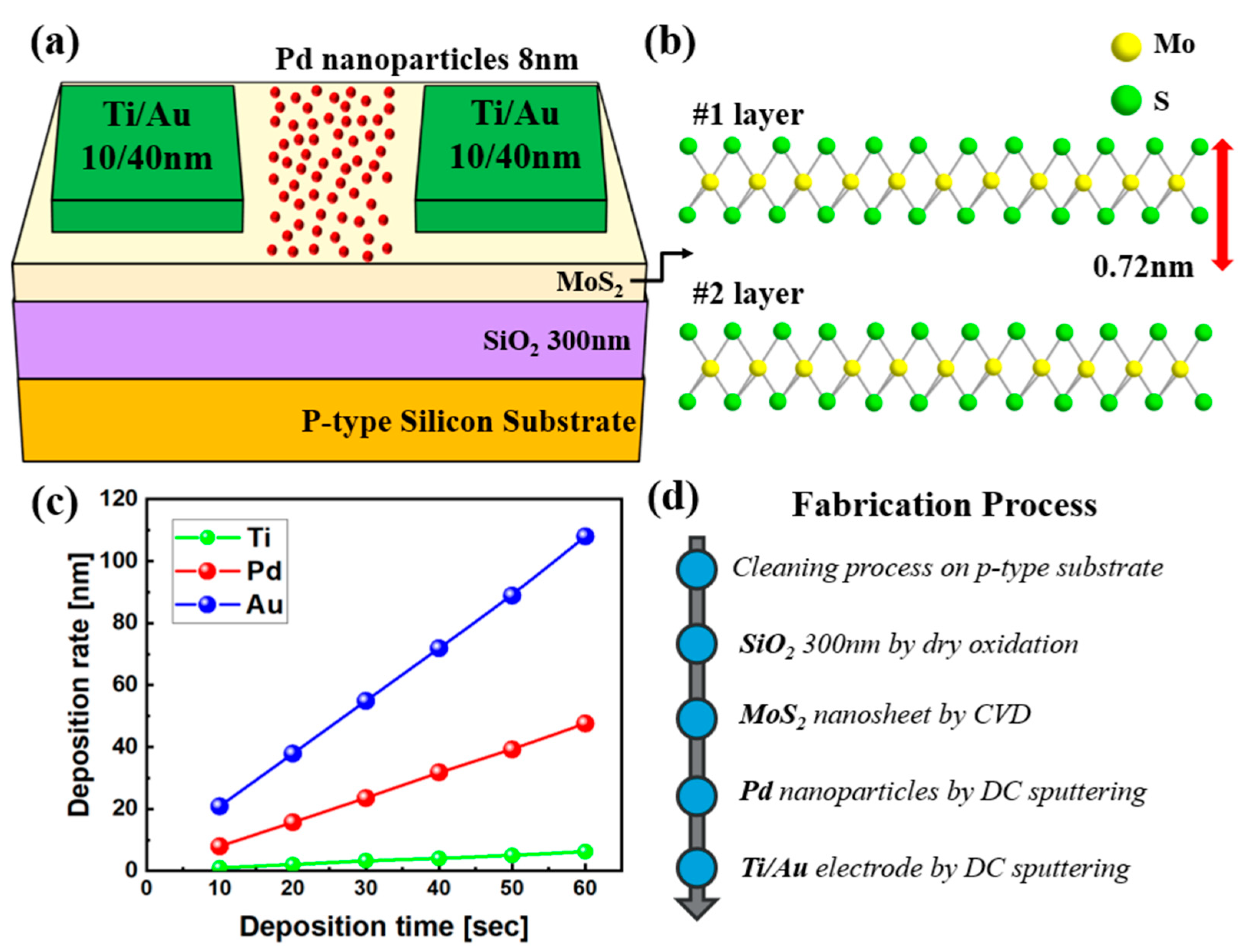
The memristor based on Pd-MoS2 nanocomposites was fabricated as shown in Figure 2a. Initially, a sequence of cleaning steps was performed using acetone, isopropyl alcohol, and deionized water to remove organic solvents present on the p-type silicon substrate. After drying with N2 gas, SiO2 of 300 nm was formed on the p-type substrate by dry oxidation. For the synthesis of the MoS2 switching layer, a CVD method was applied by introducing MoO3 power (18mg) and S powder (120mg) into a furnace. During the growth of MoS2, the argon (Ar)-gas flow rate, central heating zone temperature, and upstream S zone temperature were set at 25 SCCM, 750 °C, and 180 °C, respectively. Figure 2b illustrates the nanostructures of monolayer MoS2 (≈ 0.72 nm) and multilayer MoS2 (≈ 1.44 nm). Subsequently, a multilayer MoS2 film was fabricated on the SiO2. Figure 2c shows the deposition rate of the DC sputter equipment. Following photo-lithography pattering, Pd nanoparticles were mixed with MoS2 nanosheets to form the switching channel layer. Pd, titanium (Ti), and gold (Au) were fabricated using 99.99% pure targets. DC sputter deposition conditions were kept constant with an Ar-gas flow rate, DC power, chamber working pressure, and substrate temperature set at 30 SCCM, 100 W, 1.4 × 10⁻³ Torr, and a range of 0 to 60 °C, respectively. To apply the top electrode (TE) and bottom electrode (BE) as two-terminal electrodes, Ti/Au were deposited with thicknesses of 10 nm/40 nm to complete the fabrication of the RRAM device.

3.2. Raman Spectroscopy

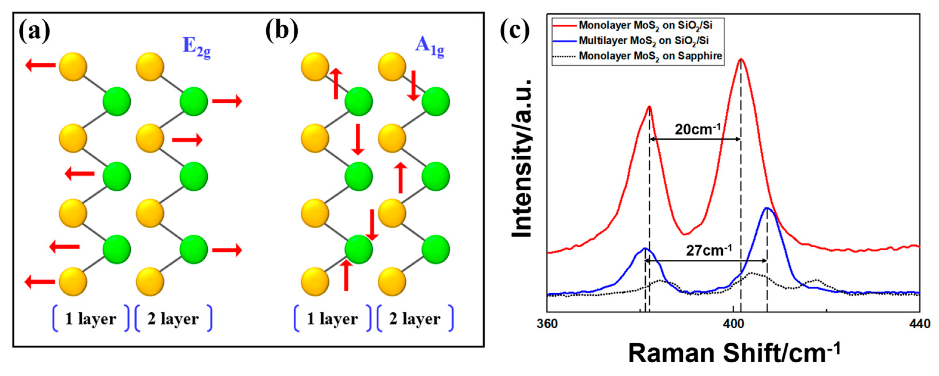
Raman data spectroscopy precisely analyzes the exact number of layers, structural properties, and energy of vibration modes, which provides important insights into nanomaterials [20]. In Raman data measurements, Figure 3a,b focus on the crucial peaks associated with two vibrational modes (E2g and A1g) of MoS2. The E2g peak of MoS2 is significantly influenced by its crystalline structure, particle size, and thickness during growth. Additionally, the A1g peak vibration is related to the crystalline structure and thickness of MoS2, serving as an indicator of material quality. Figure 3c describes the Raman spectrum, an important indicator for understanding the physical properties and structure of monolayer & multilayer MoS2 on SiO2/Si substrate. For monolayer MoS2, the E2g and A1g peaks were observed at 382 cm-1 and 402 cm-1, respectively. In contrast, for multilayer MoS2, these peaks were appeared at 380 cm-1 and 407 cm-1, respectively. The E2g peak (in-plane vibrational mode) involves parallel vibrations of Mo and S atoms within MoS2. Also, the A1g peak (out-of-plane vibrational mode) encompasses the vertical vibrations of S atoms [21]. The distance between the two peaks acts as an indicator that directly represents the number of layers of MoS2. It has been confirmed that the distance between the peaks increases due to high-intensity vibrations as the number of layers increases.

3.3. Photoluminescence Mapping

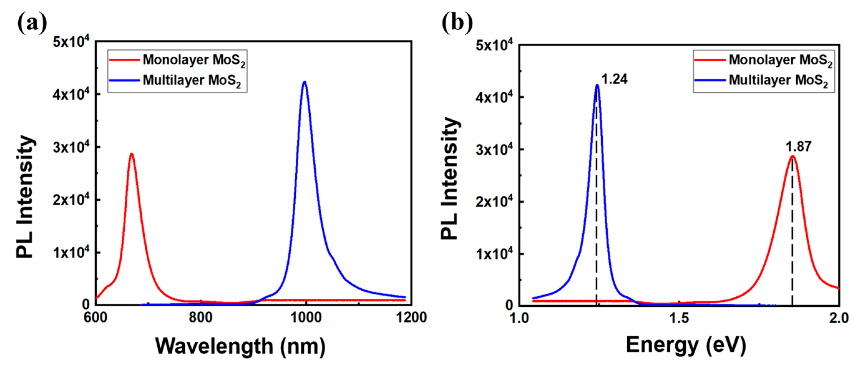
Photoluminescence (PL) spectroscopy is applied to determine the material’s electronic states, structural characteristics, and bandgap based on the energy of emitted photons. In Figure 4a, PL signals were observed at room temperature using a 532nm laser. For monolayer MoS2 samples, it can be observed that the PL intensity exhibits a lower peak compared to multilayer MoS2. Through PL Mapping, MoS2 synthesized by CVD techniques exhibits high-quality crystalline growth. Planck’s constant (6.62 × 10⁻³⁴ J·s), the speed of light (2.99 × 10⁸ m/s), and wavelength are denoted as h, c, and λ, respectively, and equation (1) is used to calculate the energy of emitted photons.
E = h × c λ   1240 λ   ( e V )
Figure 4a shows that the PL peak of monolayer MoS2 appears at 660 nm, while that of multilayer MoS2 is located at 995 nm. Applying the conversion relationship between wavelength and photon energy, Figure 4b reveals that the bandgap of monolayer MoS2 is extracted as 1.87 eV, while that of multilayer MoS2 is observed to be 1.24 eV. Consequently, this aligns with the bandgap range typically known through research [22]. The intensity of the PL peak represents the efficiency of the light emission process occurring in MoS2 [23].

4. Results and Discussions

The resistive switching (RS) model within RRAM devices has typically been applied by the application of two main theoretical mechanisms. Specifically, the electrochemical metallization (ECM) model is known for the formation of conductive bridges by metal ions within the channel, while the valence change mechanism (VCM) model regulates the conductive filaments (CFs) through the creation and recombination of oxygen vacancies induced by an electric field. Recently, new concept models have been proposed to control the current paths by generating ions or vacancies by various channel materials or nanomaterials applied to RRAM cells [24,25].

4.1. Resistive Switching Mechanisms

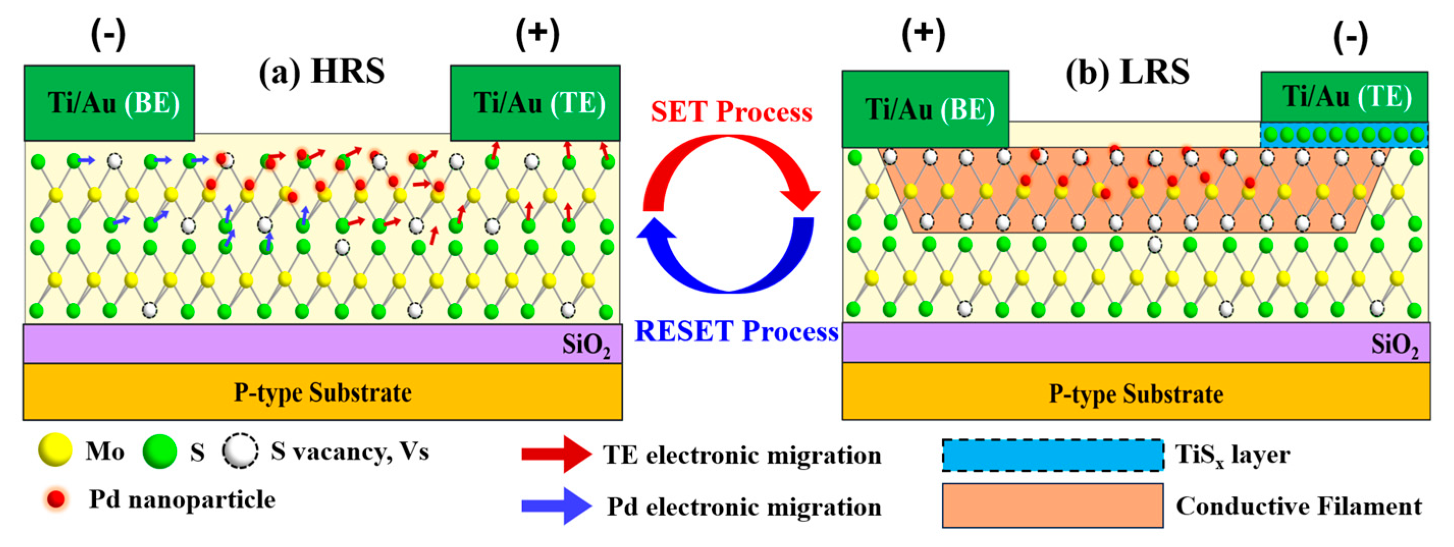
The RS mechanism for Pd coated multilayer MoS2 RRAM device is illustrated in Figure 5. An electrical RS operation (electronic by TE & electronic by Pd) has been conceived to form the S vacancies (Vs) filaments in the current paths [26]. Figure 5a shows the initial high resistance state (HRS) with low concentrations of Vs distributed in the switching layer. When a forward voltage bias is applied to the TE, the switching layer collapses and negatively charged S ions are accumulated under the TE. By the SET process, the TiSx layer is formed by reacting with Ti as shown in Figure 5b [27]. Additionally, S ions, which are far from TE, form Vs filaments due to an electrical field caught in Pd nanoparticles. When a conductive filament connects the TE and BE, the RRAM cells cause a low resistance state (LRS). The migration of S ions in the active channel layer occurs as follows. S ions that are far from TE are not subject to the electronic by TE effect. However, S ions are formed by the electric field effect of Pd nanoparticles [28]. When the TE and BE are connected by the CFs, the RRAM devices cause the LRS. When a negative voltage bias is applied to the TE, S ions migrate into the MoS2 layer. As a result, the TiSx layer decreases in size, and the CFs rupture, causing a transition to an HRS (RESET process).

4.2. I-V Measurement

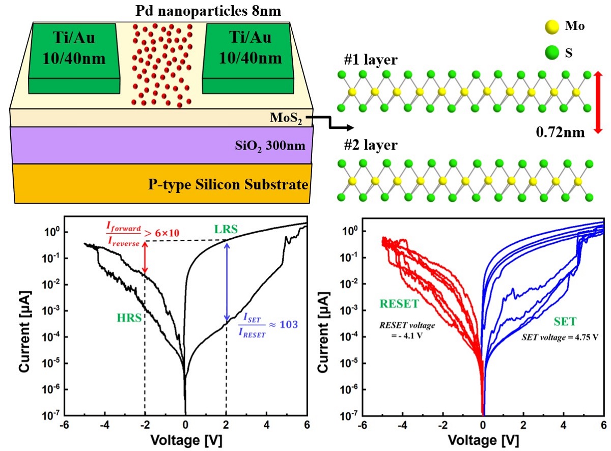
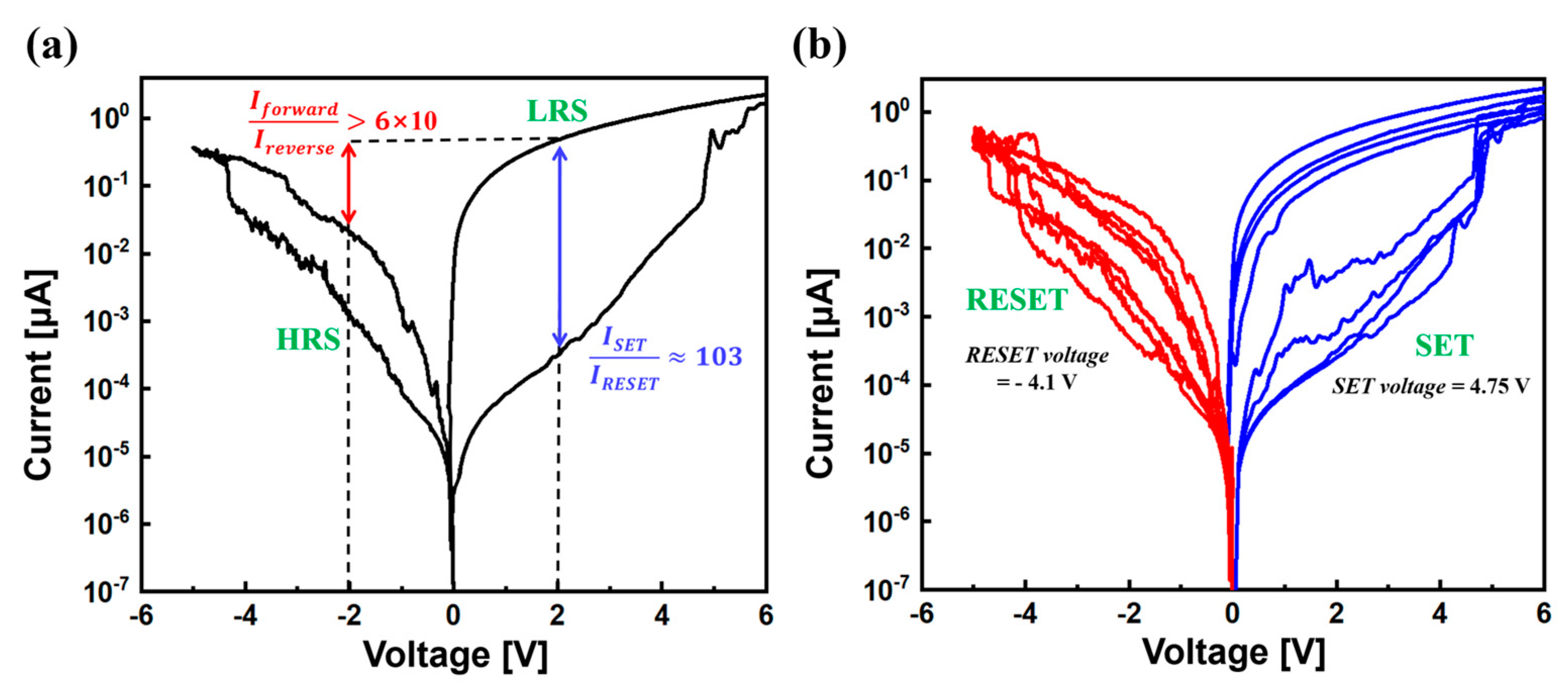
The fabricated Pd-MoS2 nanocomposites RRAM were measured by a vacuum probe station and semiconductor parameter analyzer (HP4156A). Bias was applied to the TE with the BE grounded throughout the measurement process. Compliance current was set to a value of 20 μA to suppress overcurrent through the device. Figure 6a displays the measured current-voltage (I-V) characteristics of the RRAM device consisting of an ideal switching layer with multilayer MoS2 (= 2 layers) and Pd nanoparticles (= 8 nm). Asymmetrical bipolar switching behavior was observed due to the Schottky barrier at the interface of multilayer MoS2 and the electrode. The Schottky contact at the MoS2/Ti interface prevented reverse current and allowed forward current to flow. In both the forward and reverse LRS, the rectifying current ratio (> 6 × 10) was assessed by comparing the forward current (Iforward) of 0.612 μA at a forward voltage of +2V with the reverse current (Ireverse) of 0.012 μA at a reverse voltage of -2V. Selector-integrated RRAM controlled leakage current and exhibited self-rectifying operation. The RRAM with Pd decorated MoS2 channel structure demonstrated a bipolar switching with continuous and stable RS behavior (VSET = +4.75 V, VRESET = -4.1 V), as shown in Figure 6b. When extracting SET and RESET currents, ISET and IRESET were found to be less than 1 μA, indicating excellent memory performance, such as low-power operation, a high memory window on/off ratio (≈ 103), and nanoscale device fabrication. Furthermore, it appears that the issue of leakage current due to cross-talk in RRAM array cells has been addressed, and high-density memory array stacking is feasible. Table 1 summarizes the comparison of device stack structure, nanocomposites-based MoS2, on/off ratio, and other parameters for MoS2 switching layer RRAM.

5. Conclusions

This research work demonstrates a memristive RRAM based on Pd decorated multilayer MoS2 nanocomposites solution. By optimizing Pd nanoparticles deposition (DC sputter) and MoS2 nanosheets synthesis (CVD), we contributed to the electrical migration of Vs and TiSx formation in the switching layer. MoS2/Ti contact forms sufficient Schottky barriers to perform nonlinear I-V switching characteristics. Pd-MoS2 RRAM, which consists of self-integration without a selector device, derives a high memory window (≈ 103) and the rectifying current ratio (> 6 × 10) of asymmetric LRS. Nanocomposites-based RRAM should discuss leakage current by cross-talk in nanoscale cell fabrication and high-density 3D stack arrays. Finally, the application of a 2D nanomaterial memristor platform presents a direction for emerging memory devices and intelligent memristor fields.

Acknowledgments

This research was supported by the National R&D Program through the National Research Foundation of Korea (NRF) funded by the Ministry of Science and ICT (NRF-2022M3I7A1078936) and this research was supported by “Regional Innovation Strategy (RIS)” through the National Research Foundation of Korea (NRF) funded by the Ministry of Education (MOE)(2022RIS-005).

References

  1. Zhou, Jiantao, Kuk-Hwan Kim, and Wei Lu. “Crossbar RRAM arrays: Selector device requirements during read operation.” IEEE Transactions on Electron Devices 61.5 (2014): 1369-1376.
  2. Zhang, Leqi, et al. “On the optimal ON/OFF resistance ratio for resistive switching element in one-selector one-resistor crosspoint arrays.” IEEE Electron Device Letters 36.6 (2015): 570-572.
  3. Wang, Xue-Feng, et al. “Interface engineering with MoS2–Pd nanoparticles hybrid structure for a low voltage resistive switching memory.” Small 14.2 (2018): 1702525.
  4. Govoreanu, Bogdan, et al. “A-VMCO: A novel forming-free, self-rectifying, analog memory cell with low-current operation, nonfilamentary switching and excellent variability.” 2015 Symposium on VLSI Technology (VLSI Technology). IEEE, 2015.
  5. Luo, Qing, et al. “Self-rectifying and forming-free resistive-switching device for embedded memory application.” IEEE Electron Device Letters 39.5 (2018): 664-667.
  6. Chen, Ying-Chen, et al. “Analog synaptic behaviors in carbon-based self-selective RRAM for in-memory supervised learning.” 2021 IEEE 71st Electronic Components and Technology Conference (ECTC). IEEE, 2021.
  7. Bai, Yue, et al. “Stacked 3D RRAM array with graphene/CNT as edge electrodes.” Scientific reports 5.1 (2015): 13785.
  8. Ye, Cong, et al. “Physical mechanism and performance factors of metal oxide based resistive switching memory: a review.” Journal of Materials Science & Technology 32.1 (2016): 1-11.
  9. Mullani, Navaj, et al. “Improved resistive switching behavior of multiwalled carbon nanotube/TiO2 nanorods composite film by increased oxygen vacancy reservoir.” Materials Science in Semiconductor Processing 108 (2020): 104907.
  10. Ryu, Ji-Ho, and Sungjun Kim. “Artificial synaptic characteristics of TiO2/HfO2 memristor with self-rectifying switching for brain-inspired computing.” Chaos, Solitons & Fractals 140 (2020): 110236.
  11. Rodriguez-Fernandez, Alberto, et al. “Resistive switching with self-rectifying tunability and influence of the oxide layer thickness in Ni/HfO2/n+-Si RRAM devices.” IEEE Transactions on Electron Devices 64.8 (2017): 3159-3166.
  12. Ryu, Hojeong, and Sungjun Kim. “Self-Rectifying Resistive Switching and Short-Term Memory Characteristics in Pt/HfO2/TaO x/TiN Artificial Synaptic Device.” Nanomaterials 10.11 (2020): 2159.
  13. Chand, Umesh, et al. “Mechanism of nonlinear switching in HfO2-based crossbar RRAM with inserting large bandgap tunneling barrier layer.” IEEE Transactions on Electron Devices 62.11 (2015): 3665-3670.
  14. Kim, Hee-Dong, Sungho Kim, and Min Ju Yun. “Self-rectifying resistive switching behavior observed in Al2O3-based resistive switching memory devices with p-AlGaN semiconductor bottom electrode.” Journal of Alloys and Compounds 742 (2018): 822-827.
  15. K. Young Lae, et al. “Voltage-switchable photocurrents in single-walled carbon nanotube silicon junctions for analog and digital optoelectronics,” Nature Photonics, Vol. 8, No. 3, pp. 239-243, 2014.
  16. Luo, Yifan, and Chao Zhang. “Pt-activated TiO2-MoS2 nanocomposites for H2 detection at low temperature.” Journal of Alloys and Compounds 747 (2018): 550-557.
  17. Bhattacharjee, Shubhadeep, et al. “Insights into multilevel resistive switching in monolayer MoS2.” ACS applied materials & interfaces 12.5 (2020): 6022-6029.
  18. Shi, Y. et al. Van der Waals epitaxy of MoS2 layers using graphene as growth templates. Nano letters 12, 2784–2791 (2012).
  19. Ma, X. & Shi, M. Thermal Evaporation Deposition of Few-layer MoS2 Films. Nano-Micro Letters 5 (2013).
  20. Lee, Changgu, et al. “Anomalous lattice vibrations of single-and few-layer MoS2.” ACS nano 4.5 (2010): 2695-2700.
  21. Han, Tao, et al. “Probing the optical properties of MoS2 on SiO2/Si and sapphire substrates.” Nanomaterials 9.5 (2019): 740.
  22. Chow, Philippe K., et al. “Wetting of mono and few-layered WS2 and MoS2 films supported on Si/SiO2 substrates.” ACS nano 9.3 (2015): 3023-3031.
  23. Han, Tao, et al. “Probing the optical properties of MoS2 on SiO2/Si and sapphire substrates.” Nanomaterials 9.5 (2019): 740.
  24. Rehman, Muhammad Muqeet, et al. “Decade of 2D-materials-based RRAM devices: a review.” Science and technology of advanced materials 21.1 (2020): 147-186.
  25. Ryu, Hojeong, and Sungjun Kim. “Self-Rectifying Resistive Switching and Short-Term Memory Characteristics in Pt/HfO2/TaO x/TiN Artificial Synaptic Device.” Nanomaterials 10.11 (2020): 2159.
  26. Li, Da, et al. “MoS2 memristors exhibiting variable switching characteristics toward biorealistic synaptic emulation.” ACS nano 12.9 (2018): 9240-9252.
  27. Liu, Lifu, et al. “Robust resistive switching in MoS2-based memristor with Ti top electrode.” Applied Surface Science 605 (2022): 154698.
  28. Monama, Nkwe Oscar. Electronic structure studies of pallandium sulphide (PdS) and platinum (pt) ternaries. Diss. University of Limpopo (Turfloop Campus), 2008.
  29. Bessonov, Alexander A., et al. “Layered memristive and memcapacitive switches for printable electronics.” Nature materials 14.2 (2015): 199-204.
  30. Sangwan, Vinod K., et al. “Gate-tunable memristive phenomena mediated by grain boundaries in single-layer MoS2.” Nature nanotechnology 10.5 (2015): 403-406.
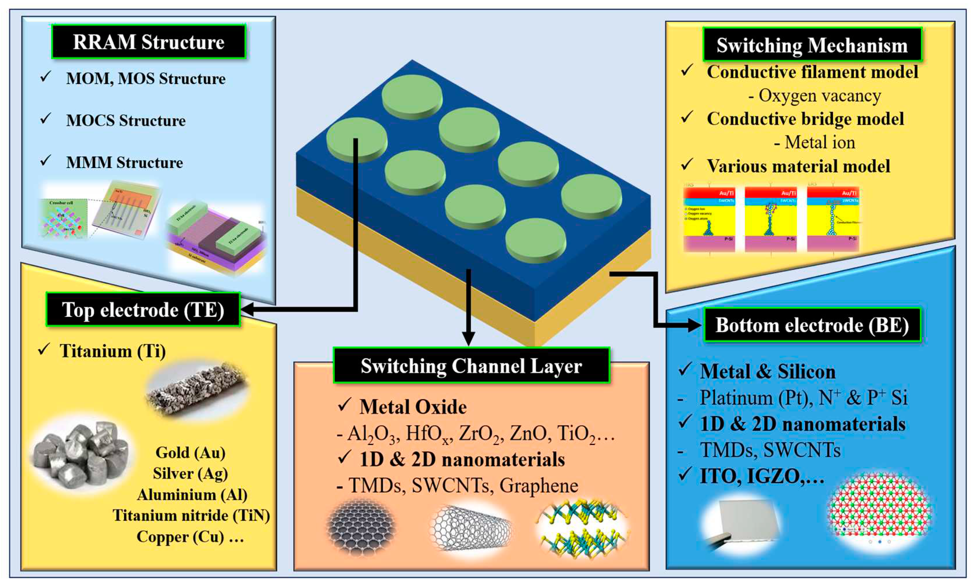
Figure 1. Illustration of various materials for RRAM device applications.
Preprints 87736 g001
Figure 2. (a) The schematic of Pd-MoS2 RRAM device; (b) The structure of monolayer or multilayer MoS2 lattice layer; (c) Deposition rates of various metals (Ti, Pd, and Au) by DC sputter; (d) Fabrication process flow chart of the proposed RRAM architecture.
Preprints 87736 g002
Figure 3. (a) E2g band in-plane vibration of MoS2; (b) A1g band out-of-plane vibration of MoS2; (c) Raman spectrum of monolayer MoS2 and multilayer MoS2 on the SiO2/Si.
Preprints 87736 g003
Figure 4. Scanning PL spectrum of monolayer MoS2 and multilayer MoS2; (a) wavelength; (b) Energy bandgap of the emitted photon.
Preprints 87736 g004
Figure 5. RS behavior of the Pd decorated multilayer MoS2 RRAM device. (a) HRS (initial state); (b) LRS (after the SET process). The red and blue lines arrows show the S ion migration direction (electronic by TE & electronic by Pd).
Preprints 87736 g005
Figure 6. I-V characteristics of Pd-MoS2 RRAM. (a) Self-rectifying RS operation. Rectifying current ratio was observed Iforward (@ V = +2 V) and Ireverse (@ V = -2 V). Memory window (≈ 103) was extracted; (b) I-V characteristics of Pd-MoS2 RRAM for repeated voltage (-6V to 6V) sweeps.
Preprints 87736 g006
Table 1. This is a table. Tables should be placed in the main text near to the first time they are cited.
TE & BE Switching layer On/Off ratio Rectifying ratio Ref
ITO & ITO HfOx/Pd-MoS2 ≈ 102 - [3]
Au & Au MoS2 ≈ 105 - [17]
Au/Ti & Au/Ti MoS2 ≈ 101 - [26]
Ti & Pt MoS2 ≈ 102 - [27]
Ag & Ag MoS2/MoOx ≈ 106 - [29]
Au & TiN HfOx/MoS2/TiOx ≈ 106 - [30]
Au/Ti & Au/Ti Pd-MoS2 ≈ 103 > 6 × 10 This work.
Disclaimer/Publisher’s Note: The statements, opinions and data contained in all publications are solely those of the individual author(s) and contributor(s) and not of MDPI and/or the editor(s). MDPI and/or the editor(s) disclaim responsibility for any injury to people or property resulting from any ideas, methods, instructions or products referred to in the content.
Copyright: This open access article is published under a Creative Commons CC BY 4.0 license, which permit the free download, distribution, and reuse, provided that the author and preprint are cited in any reuse.
Prerpints.org logo

Preprints.org is a free preprint server supported by MDPI in Basel, Switzerland.

Subscribe

© 2024 MDPI (Basel, Switzerland) unless otherwise stated