1. Introduction
Hafnium, a transition metal known for its high melting point and good electronic properties, has attracted significant attention from scientists in the fields of material science and nanotechnology. Its unique characteristics make it a promising candidate for a variety of applications, including superconducting nanoelectronics. To unleash the potential of hafnium, an investigation at ultra-low temperatures is required. It is also critical to understand how its properties will change upon contact with thin films of other metals.
This article will describe ultra-low temperature measurements of hafnium thin films and their combinations with normal metal films, exploring the problems and insights generated by such experiments.
The purpose of this work is to study the properties of hafnium thin films, from which it is planned to create a microcalorimeter based on a Transition-Edge Sensor (TES). The material for TES requires a critical temperature below 100 mK and a narrow width of the superconducting transition. Also, for the successful operation of this detector, the properties of thin film of its material must be stable over time.
While the superconducting temperature of materials for TES tends to become lower in order to increase its sensitivity, see, for example, [
1,
2,
3,
4], hafnium has been poorly studied for this application. Also, the possibility to turn the transition temperature below 100 mK makes hafnium a suitable superconductor for use in single photon counters [
5,
6,
7]. The critical temperature of bulk hafnium is close enough to the required one [
4,
8,
9]. It is possible to achieve its suppression within the necessary limits by depositing layers of normal metals on films of pure hafnium. Commonly used materials are silver and gold.
By now there are just a few works investigating the properties of hafnium films. Moreover, the data on the transition temperature vary greatly in the ranges from ~50–350 to 100–450 mK [
4,
9], and presumably depends on a material contamination, specific for each case.
Thus, in [
9], the dependence of the critical temperature on the argon pressure in the chamber is given, while the critical temperature varies from 250 to 450 mK.
At the same time, in [
8], for bulk hafnium, the critical temperature is 137–205 mK with a transition width of 2 mK.
It [
3] the superconducting transition temperature of hafnium thin films is about 200 mK. The authors of this work carried out experiments with a TES detector 25 by 25 µm in size and approximately 30 nm thick, made of hafnium. In the same paper, a conventional hafnium film with a thickness of 30 nm absorbs infrared radiation with a wavelength of 850 nm (352.7 THz) with an efficiency of 40%. This value was increased to 85% by formation of special optical cavities.
A superconductor such as iridium can also be used to accomplish the tasks set [
10,
11,
12]. Iridium has superconducting properties close to hafnium; its critical temperature is 112 mK [
10]. It also allows changing its critical temperature by using the proximity effect [
2,
11,
13,
14]. But there are difficulties with depositing iridium to the substrate; it is a more refractory and dense metal than hafnium. Therefore, it requires a magnetron sputtering machine and a heating of a substrate [
10,
12]. In addition, iridium is much more expensive compared to hafnium.
It is also shown [
15] that it is possible to use tungsten in order to obtain the critical temperature in the required range. However, tungsten has its own drawbacks, as several crystal modifications, which can turn into each other during thermocycling [
3]. In contrast, hafnium has a hexagonal close-packed crystallographic structure, which is not as susceptible to temperature loads as tungsten with its A15 crystallographic structure [
15].
During our measurements, we encountered changes in the properties of the films, composed of one and two layers, over time. This change of properties was analyzed in the last section of this publication. The presence of a normal metal layer can be a reason for a long-term diffusion or other effects at the border between layers, which change the structure of the films and as a result its superconducting properties.
2. Measuring Setup and Holder
Measurements were carried out in a standard dilution cryostat Triton 200 from Oxford Instruments with a minimal temperature of 10 mK. Film samples were mounted on the lower plate of the cryostat under the dilution chamber.
A holder, designed for 10 samples, with clamping contacts (made of brass and plated with 3 µm of gold) was made. The sample holder is designed for films with sizes from 4 by 4 mm to 12 by 20 mm. The distance between the contacts is 2.54 or 5.08 mm depending on the film size.
These contacts have a number of advantages:
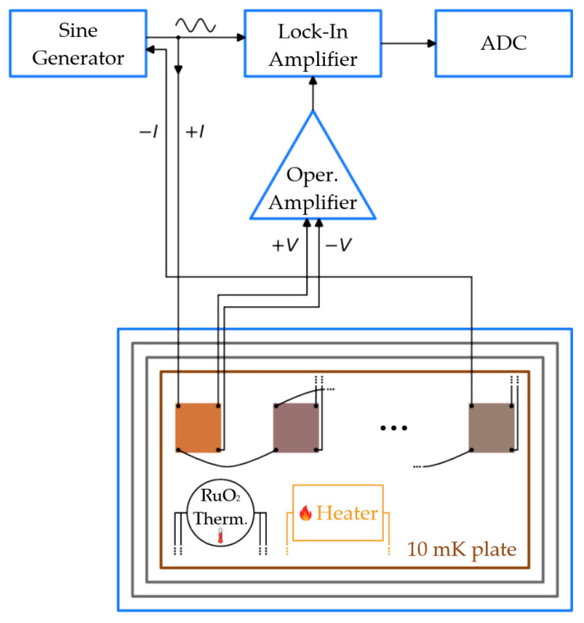
To set the current, only two contacts are used, because all samples can be connected in series. This leaves more contacts for voltage measurement (the current and voltage supply diagram is shown in
Figure 1).
The scheme of the measuring setup is shown in
Figure 1. A set of films was placed in the designed holder, which was screwed to the 10-mK cryostat plate. The films were interconnected in such a way that the current passed through all the films simultaneously. The current source was a Sine Generator in SR 830 Lock-In Amplifier. The voltage generated on the film was amplified by a factor of 1000 using an AD745 operational amplifier circuit and fed into a lock-in amplifier, which extracted its value at the chosen frequency (315 GHz). The Lock-In Amplifier generated a DC voltage corresponding to this value, which we measured using the ADC.
By dividing the voltage by the current and taking into account the gain of the Lock-In Amplifier, the film resistance can be calculated. We slowly changed the temperature of the plate to get the temperature dependence of the film resistance.
The temperature was measured with a commercial RuO2 thermometer supplied with the cryostat, calibrated with Magnicon SQUID thermometer. One temperature measurement with this thermometer takes at least 15 seconds, depending on the settings. The films were heated using a built-in heater on the 10 mK plate of the cryostat.
3. Measurement Results
In this work, hafnium films with different thicknesses in the range from 60 to 115 nm, deposited on substrates by electron beam evaporation, are investigated. Their combinations with thin layers of silver and gold are analyzed, and their effect on the critical temperature of superconducting hafnium films was studied.
The achievement of controlled low superconducting transition temperatures expands the functionality and increases the range of applicability of superconducting devices. Namely, for our research task it is necessary to reduce the critical temperature of hafnium films in order to increase the energy resolution of microcalorimeters.
All films, investigated here, were deposited using electron beam evaporation, since it was shown in [
16] that an amorphous hafnium film with a smooth surface can be obtained by this method. Also hafnium can be deposited by a magnetron sputtering, however the sputtered films appear to have less suitable properties for our goal.
We have tested three different hafnium sources with purity 99.5%, 99.9% and 99.95%. The contamination of the first source (99.5%) was investigated using a secondary-ion mass spectrometer and was found to be composed by such nonmagnetic elements as C, O and H. The films evaporated from this source were never superconducting. Two other sources (99.9% and 99.95%) gave superconducting films in most cases. Below the results of measurements are presented for films made from the most pure source 99.95% (named here as “old” for convenience) and from the source 99.9% (named as “new”). In general we did not find any noticeable difference in superconducting properties between films from ”old” and ”new” hafnium.
3.1. Resistivity Measurements of Hafnium Films
The normal state resistance is obtained as a slope in the current-voltage characteristics (IV) of samples of hafnium films. These data were used to calculate the resistivity
ρ for each sample (
Table 1).
At the room temperature the resistivity of old hafnium films (Hf ”old”) is closer to the standard value of bulk resistivity of 4 * 10
-7 Ohm*m than in the films from new hafnium. At 20 mK “new” hafnium resistivity becomes equal to the bulk value, while “old” hafnium values are one order of magnitude below it. The resistance of all measured hafnium films decreases at cooling down. This implies that there is little influence of the impurities on the electronic transport for both hafnium sources. Therefore, taking into account the temperature decrease of the resistivity and its convergence to the bulk value we can expect that the critical temperature of the films will be comparable with the values of the critical temperature of bulk hafnium indicated in [
8].
3.2. Film-by-Film Results for Old Hafnium
3.2.1. Hf Old 97 nm
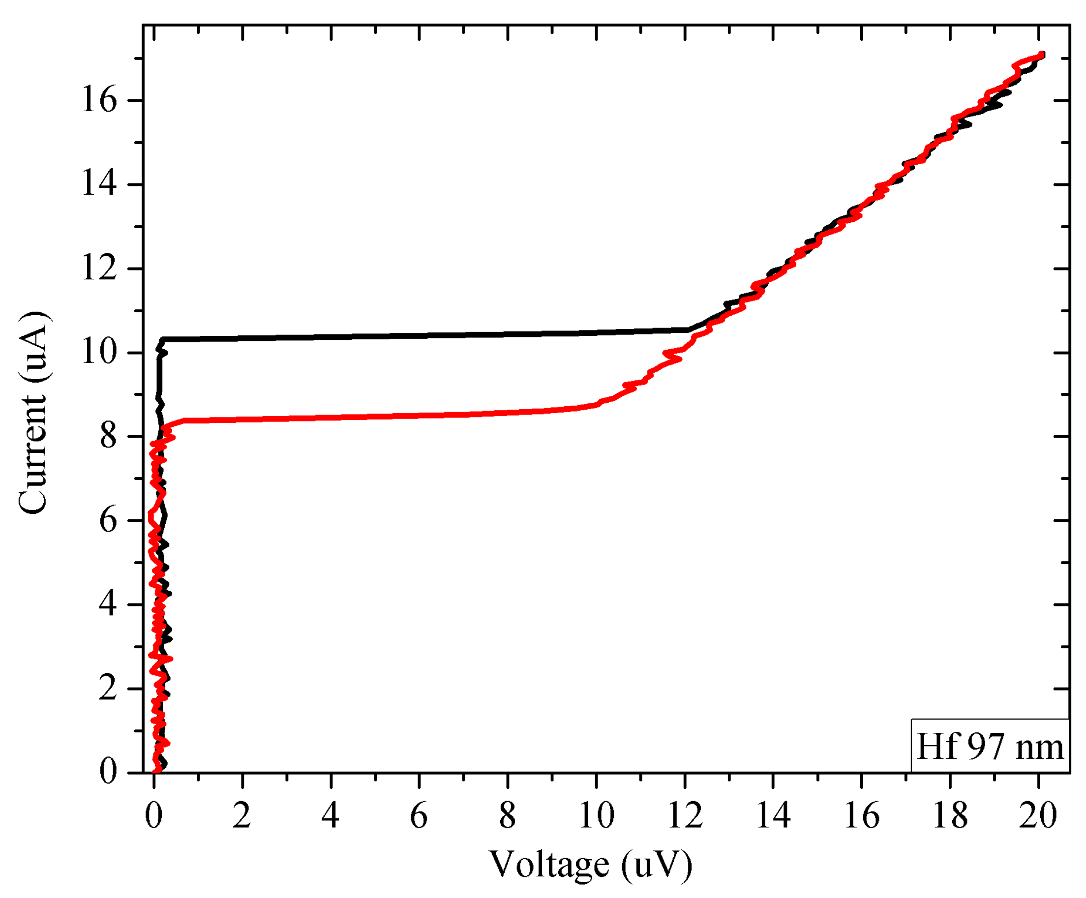
The 97 nm thick hafnium film deposited on Si substrate was measured at the temperature of 15 mK and demonstrated the typical current-voltage characteristic of a film in the superconducting state (
Figure 2). The critical current is 10.4 µA, the normal resistance after the transition to the normal state is 1.1 Ohms.
When the current increases above 10.4 µA, the film jumps into the resistive state. Such a sharp transition suggests that the observed critical current is not the true critical current of a given film, and the transition to the resistive state occurs due to the heating of the supply wires by the current, from which heat is also transferred to the film.
The hysteresis on the reverse branch is clearly visible, the return current is 8.2 µA. This indicates that the film has warmed up after the transition to the resistive state.
After measuring the IV curve, the critical temperature and the transition width were examined (
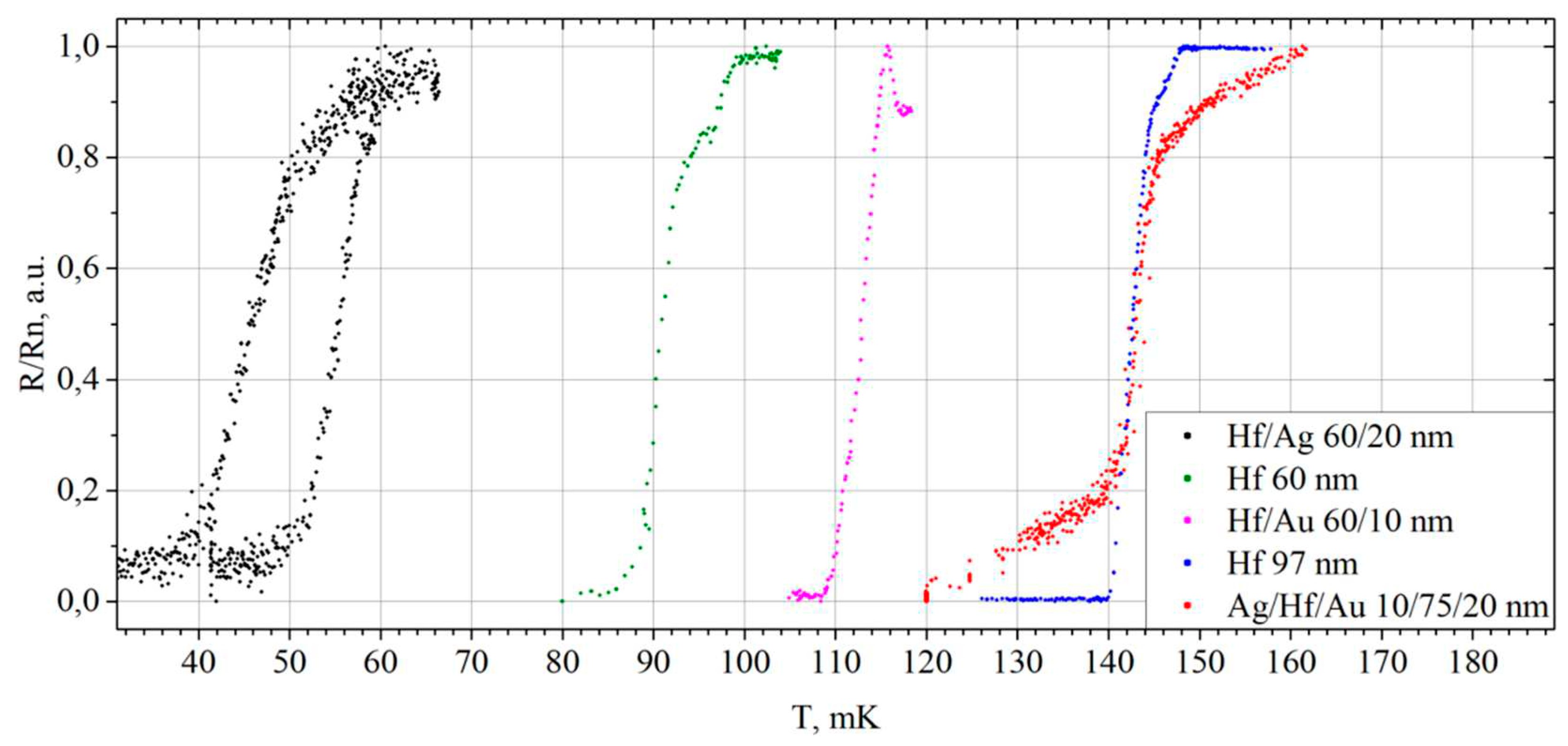
Figure 3, blue curve) from the dependence of the film resistance on the phonon temperature. A bias current of 2 µA was applied to the film, and the voltage was read using SR-830 Lock-In Amplifier. The temperature of the cryostat plate was smoothly increased using built-in heaters. Further measurements of the temperature dependence of the resistance were carried out in a similar way.
The transition from the superconducting to the resistive state started at a temperature of 140 mK, the resistance reached a plateau at a temperature of 148 mK. At this moment, the film completely returned to its normal state with a constant resistance of 1.1 Ohms. The transition turned out to be smooth and repeatable; only a small inflection was noticeable in the region of 145 mK. The main part of the transition from the superconducting to the normal state turned out to be narrow, its width was about 4 mK, indicating rather good film uniformity.
3.2.2. Hf Old 60 nm
The current-voltage characteristic of a 60 nm thick hafnium film was measured at the temperature of the cryostat of 20 mK. On the IV curve a clear non-linearity with a zero resistance branch was visible. The critical current turned out to be 8 µA, the normal resistance at 20 mK was 1.8 Ohm and the return current was 5 µA.
The dependence of the sample resistance on the phonon temperature is shown in
Figure 3 by green dots. The transition from the superconducting to the normal state began at the temperature of 87 mK and stopped changing at the temperature of 99 mK, when the film completely turned into the normal state. The transition turned out to be stepwise, inflections are noticeable in the region of 92 and 96 mK, but in the main section the width of the transition is 5 mK.
3.2.3. Hf/Au Old 60/10 nm
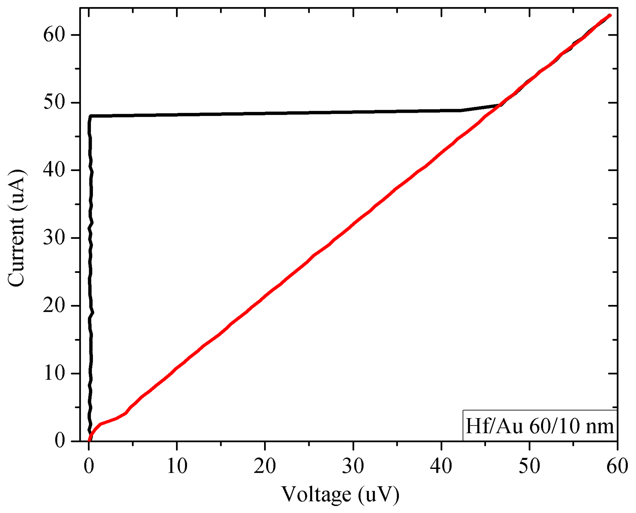
60 nm thick hafnium film with 10 nm thick layer of gold deposited on top without vacuum break was fabricated and measured at the temperature of the cryostat of 17 mK (
Figure 4). This measurement showed that the film is in the superconducting state. The critical current was 48 µA, the normal resistance in the resistive state was 0.98 Ohm.
There is a large thermal hysteresis on the reverse branch of the IV curve, the return current drops almost to zero here. This indicates a strong overheating of the film after the transition to the resistive state. At the same time, such a strong hysteresis on IV characteristics can be used to create microwave single-photon detectors based on Hf microbridges [
4,
5,
6].
Also measurements of the critical temperature and the width of the superconducting transition were performed at bias current of 0.2 µA. The transition from the superconducting to the normal state began at a temperature of 109 mK and finished at 117 mK (
Figure 3, magenta curve). The transition was relatively narrow and smooth.
It should be noted that before the complete transition to the normal state, the film resistance in a certain temperature range turned out to be higher than the normal film resistance of 0.98 Ohm. The reasons for this are not yet understood.
3.2.4. Ag/Hf/Au Old 10/75/20 nm
A three-layer film of 10 nm silver, 75 nm hafnium, and 20 nm gold was deposited. The critical current at a temperature of 20 mK was 22 µA, the normal resistance after the transition to the resistive state was 0.13 Ohm. A small thermal hysteresis was observed on the reverse branch, the return current decreased to 20 µA.
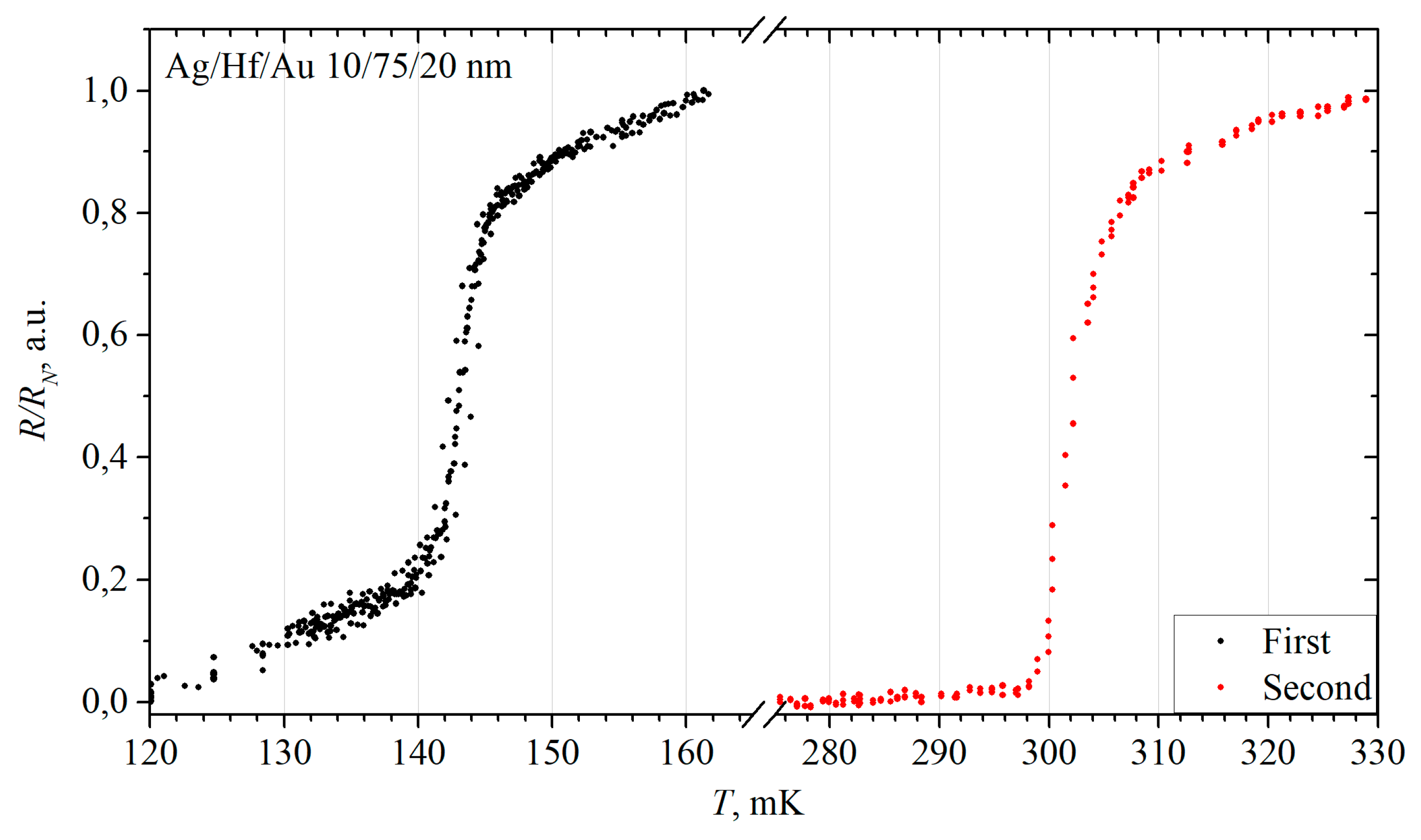
The critical temperature and transition width were measured at the bias current of 5 µA. The transition from the superconducting to the normal state began at a temperature of 142 mK and continued until the temperature of 146 mK (
Figure 3, red curve). At this point, the film has completely switched to the normal state. Although the beginning and end of the transition process were smooth, the transition itself was narrow enough.
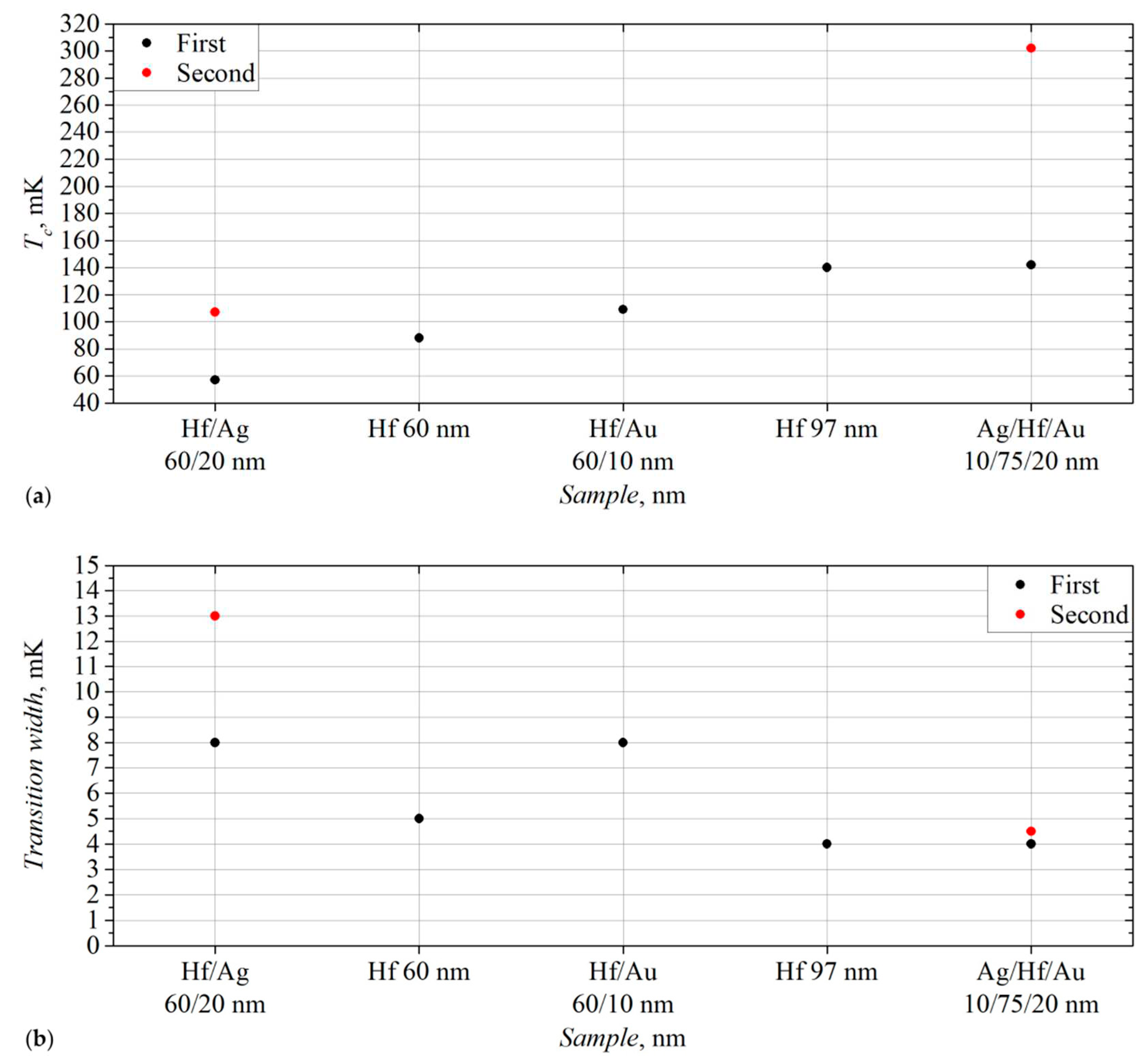
This film in the first measurement showed very good results in terms of the width of the superconducting transition. In the linear section with a constant slope, it was only 4 mK, which coincides with the width of the pure hafnium film 97 nm. Several months after deposition, this film was measured again and showed the critical temperature rise to 302 mK (
Figure 5a, red dot). The width of the transition has changed slightly (
Figure 5b, red dot).
This measurement is described in more detail in
Section 3.5 related to changes of film properties over time.
3.2.5. Hf/Ag Old 60/20 nm
60 nm hafnium film with 20 nm silver layer on top was measured in the cryostat literally immediately after electron beam deposition. From its IV curve, the critical current was found to be about 21 µA, and the normal resistance of 0.2 Ohm. On the reverse branch of the IV characteristics, the return current was 11 µA due to film heating.
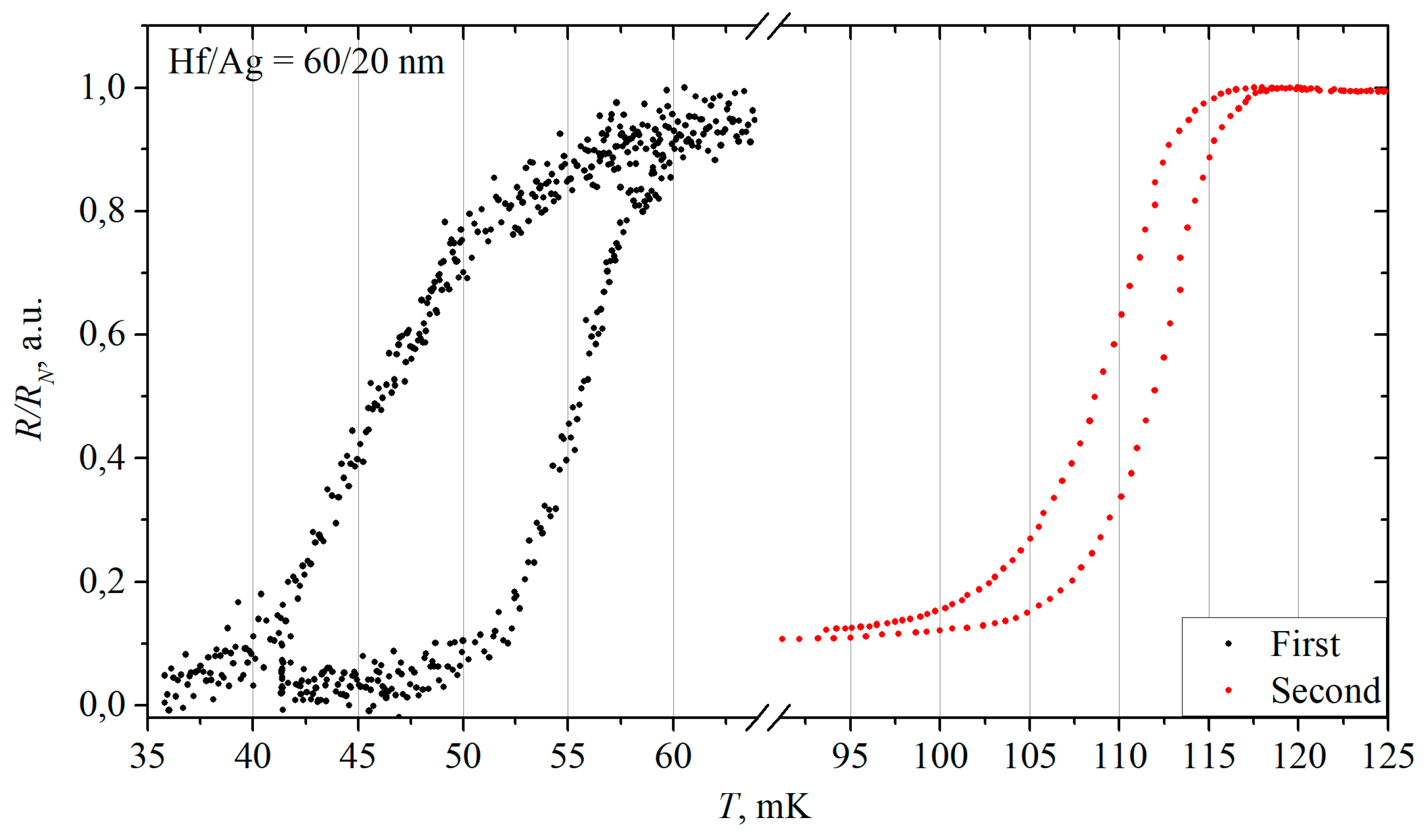
The critical temperature and transition width in the first measurement can be seen in
Figure 3 (black points). During heating, the transition from the superconducting state started at 56 mK, and the film switched to the normal state at 64 mK. On cooling, the film resistance began to drop at 52 mK, and it completely disappeared at 36 mK only.
It can be noted that the transition temperatures during heating and cooling do not coincide with each other. This effect is due to overheating of the film and it can be reduced by lowering the bias current.
Subsequently, the measurements of this film were repeated with several bias currents. Also this film, measured after a while, changed its characteristics, the critical temperature increased to 105 mK (
Figure 5a, red dot). It will be described in more detail below.
3.3. Conclusions on Measurements of Old Hafnium Films
Considering the measurement data for films containing hafnium from the old sputtering target, some dependencies can be distinguished.
Firstly, the hafnium films thinner than 60 nm are not superconducting down to 15 mK.
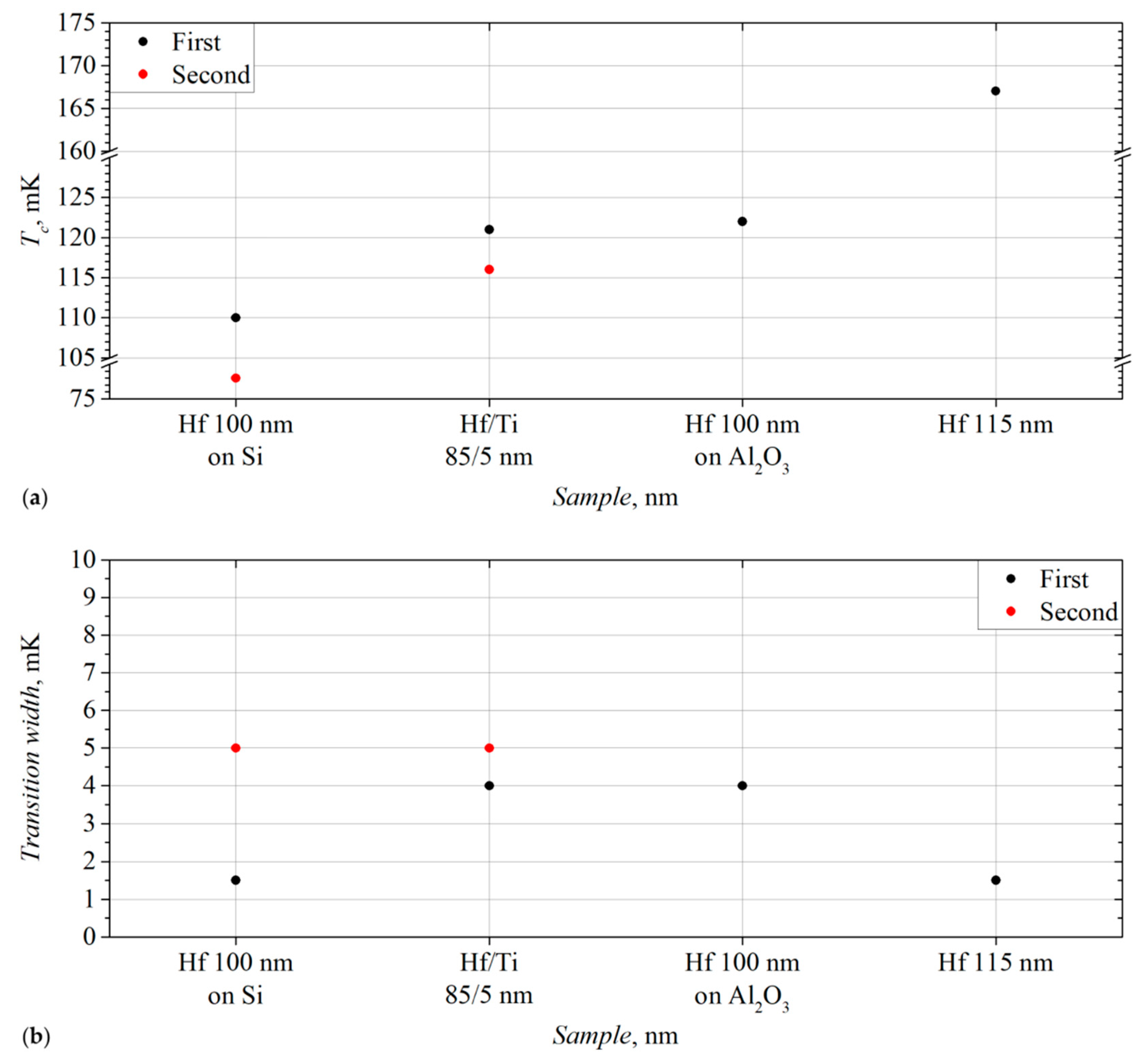
Secondly, there is a direct dependence of the hafnium superconducting transition temperature on the film thickness (
Figure 5a). The thicker the hafnium layer, the higher its critical temperature. And at the same time, the use of films of normal metals can significantly reduce the critical temperature, an example of this is the Hf/Ag 60/20 nm sample. But it should be noted that for a hafnium film with an upper layer of gold, the critical temperature turned out to be higher than for a pure hafnium film 60 nm thick.
Thirdly, there is a significant change in the characteristics (marked with red dots in
Figure 5a,b) with time in samples with silver layers, both at bottom or top. The Ag/Hf/Au 10/75/20 nm film showed a more than two times increase of the critical temperature, but at the same time retained almost the same width of the superconducting transition in the second measurement. For Hf/Ag 60/20 nm film, the second measurement cycle also demonstrated almost 100% increase in the transition temperature, and the increase in its width was more than 50%.
3.4. Films from the New Hafnium
3.4.1. Hf New 115 nm
A new hafnium source for deposition was purchased from another supplier with a declared purity of 99.9%.
The first investigated film with a thickness of 115 nm, deposited from this new source, showed an unusual IV curve and a narrow width of the superconducting transition.
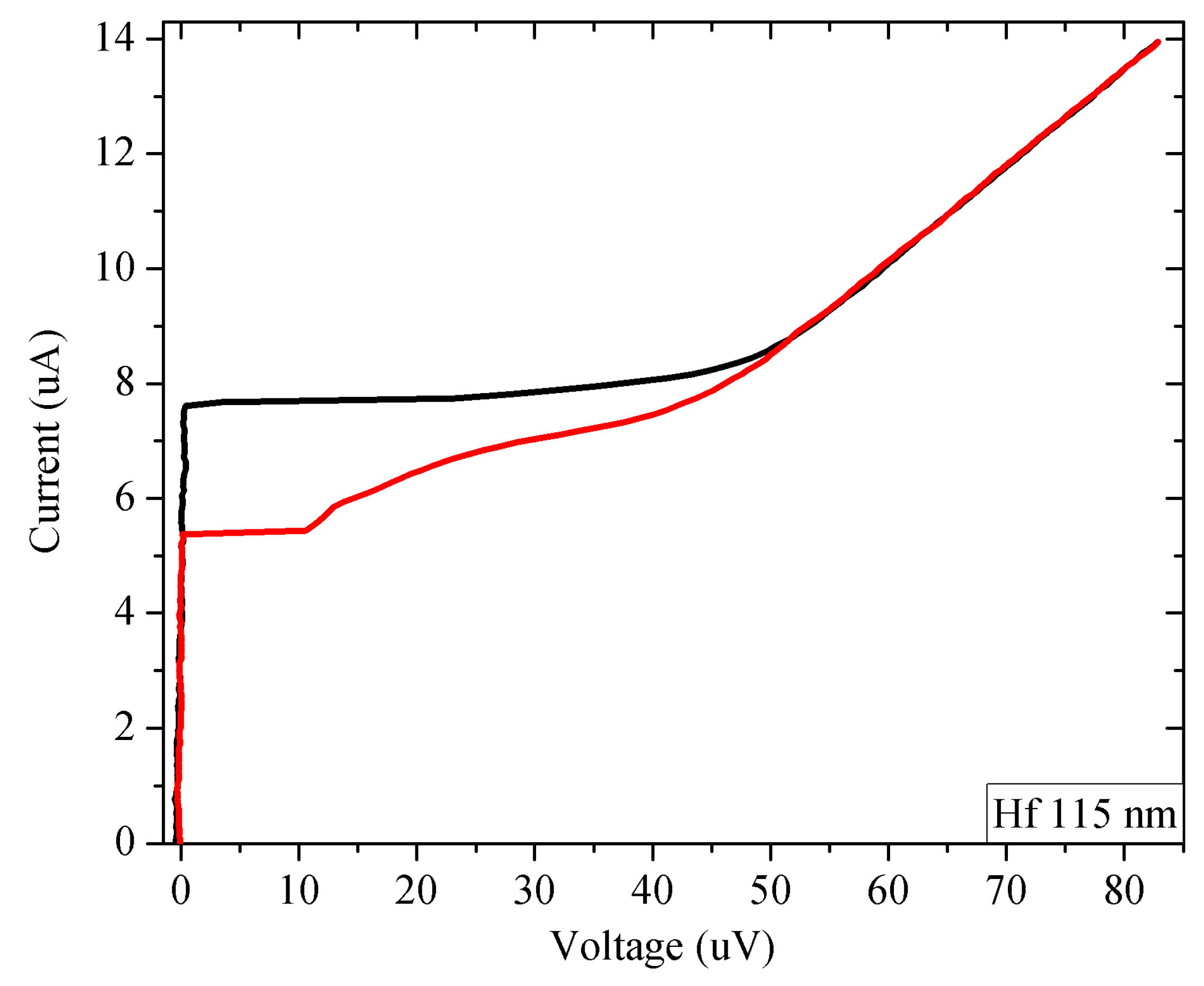
At the cryostat temperature of 17 mK, the current-voltage characteristic showed a critical current of 7.5 µA. But on the reverse branch, a strange behavior of the transition from the normal to the superconducting state was noticed, expressed by a bulge in the inclined section (
Figure 6). This feature was reproducible in all further measurements of this film.
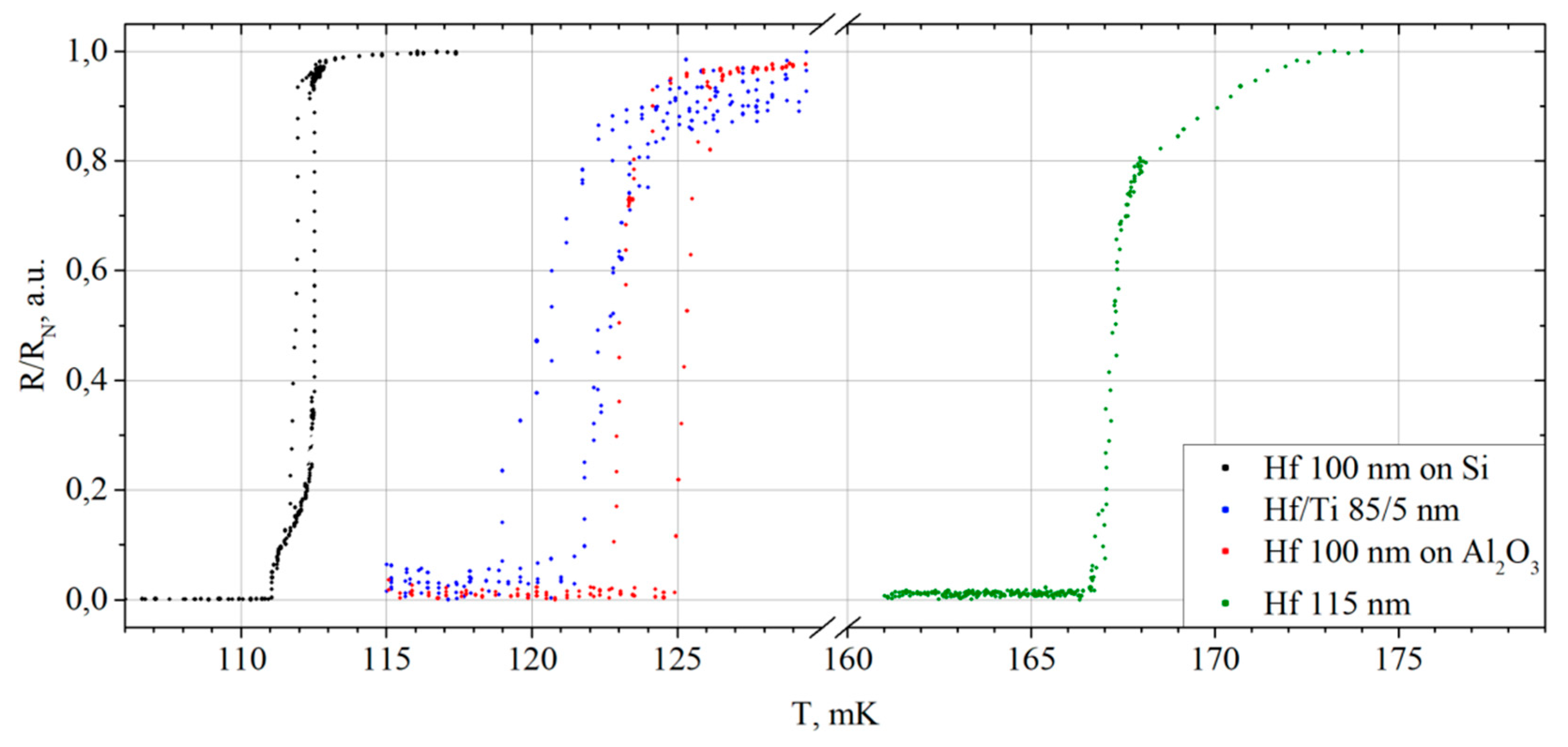
The critical temperature of the film was 166.5 mK. The transition from the superconducting to the normal state appeared as a very sharp jump, which required very careful measurement of this transition by slowly increasing the heating temperature of the plate (
Figure 7, green curve). The transition width was about 1.5 mK. Also, after a sharp transition, a region with another slope in temperature dependence of the resistance was observed.
3.4.2. Hf New 100 nm on Si and Sapphire, Hf/Ti New 85/5 nm on Si
In this section we compare the properties of 100 nm hafnium films deposited on a silicon substrate with [100] orientation of thickness 480 μm and on a sapphire substrate with [111] orientation of thickness 410 μm.
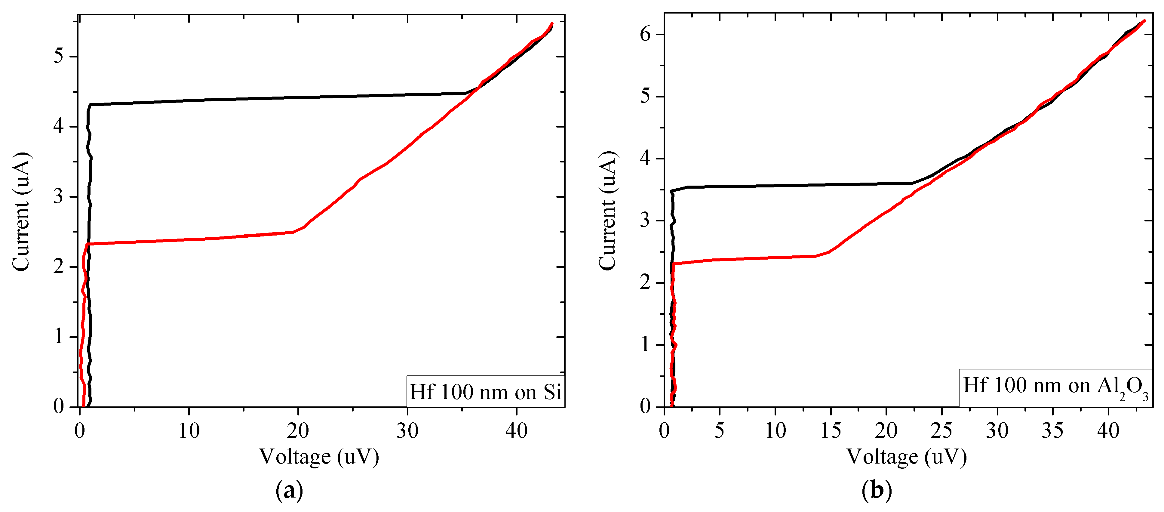
The IV curves of both films were measured at the temperature of 17 mK. The measurement showed that they both turned into the superconducting state (
Figure 8). The critical current of the film deposited on silicon was 4.4 µA, the normal resistance after the transition to the resistive state was 7.8 Ohm (
Figure 8a).
For the film on the sapphire substrate, these figures are 3.5 µA and 7.4 Ohm, respectively (
Figure 8b). It is noteworthy that the return current on the reverse branches is almost the same for both films, despite the higher critical current of the film on silicon. This confirms the expectation of better thermal conductance of sapphire which reduces thermal hysteresis.
After measuring the IV curve, the dependences of the resistance on the phonon temperature were measured for the bias current 1 µA. The resulting graphs are shown in
Figure 7. The hafnium film on silicon showed the resistance increase at 111 mK, going completely to the normal state at 113 mK. During cooling, its resistance began to decrease at 113 mK, and it turned back into the superconducting state at 110 mK (
Figure 7, black curve).
For the hafnium film on sapphire, the resistance began to increase at a temperature of 125 mK, and it completely passed to the normal state at 127 mK. Upon cooling, the transition to the superconducting state started at 125 mK, the resistance dropped to zero at 122 mK (
Figure 7, red curve). Surprisingly, the thermal hysteresis between cooling and heating was slightly stronger for the film on the sapphire substrate, while in both cases a rather sharp transition is observed.
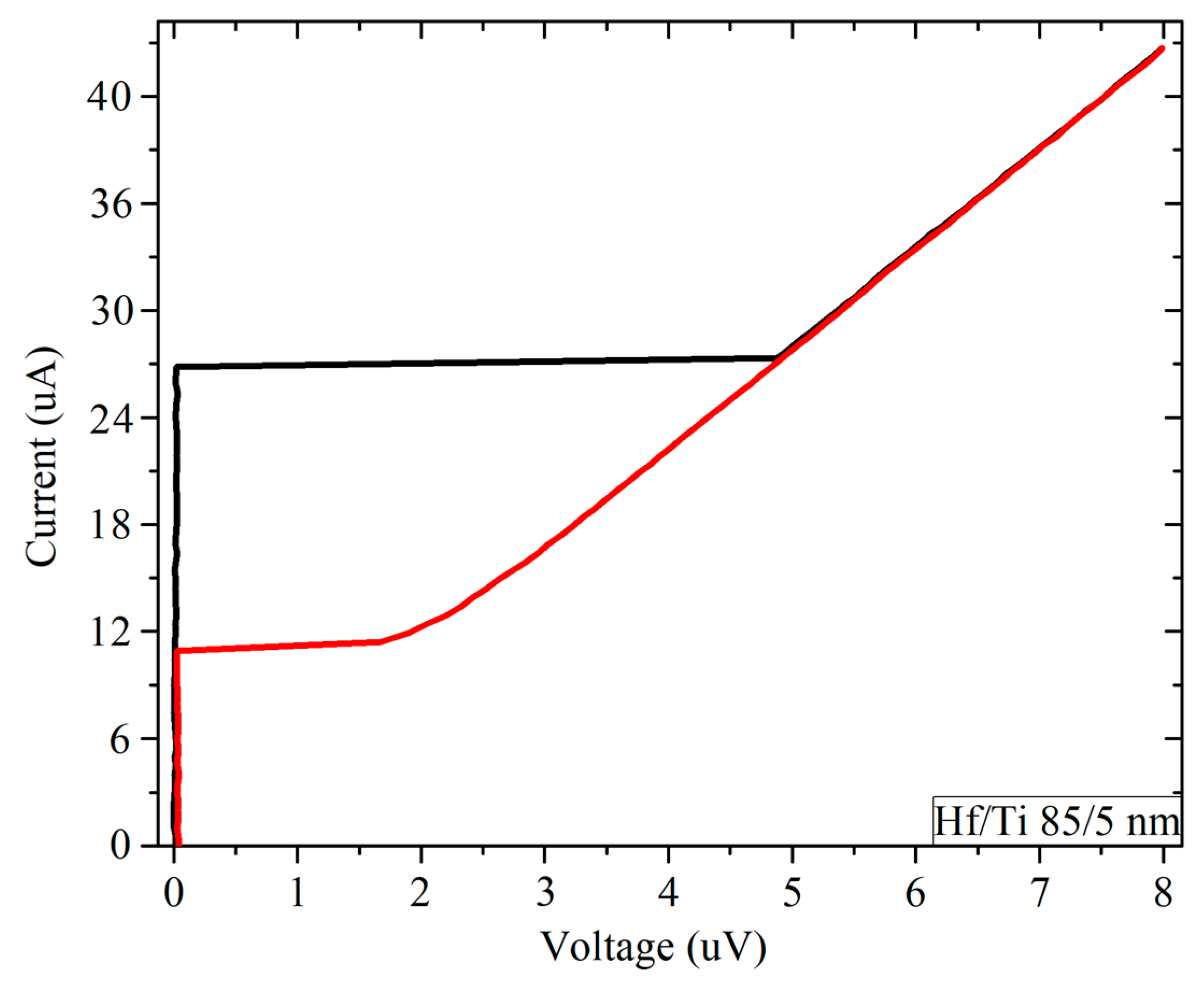
Also, along with these two films, a 85 nm thick hafnium film with a 5 nm thick titanium layer deposited on a silicon substrate was measured. The titanium layer was used to prevent the interaction of the upper hafnium border with the atmosphere, since the titanium is known for its very thin but stable oxide. The critical current of this film at temperature of 17 mK was 27 µA, and the normal resistance was about 0.2 Ohm (
Figure 9) with noticeable thermal hysteresis on the current-voltage characteristic despite the low resistance. It should be noted that the 5 nm titanium layer almost did not affect the critical temperature in comparison with pure Hf. The resistance of this film began to rise at 121 mK, at 125 mK it was already in the resistive state. On cooling, the film began to lose resistance at 124 mK, it became zero at 119 mK (
Figure 7, blue curve).
All these films showed prominent results both in terms of the superconducting transition temperatures, which are close to the goal of 100 mK, and in terms of the transition width. The obtained data for these films are presented for comparison in
Figure 10a,b.
Judging by the similarity of the obtained data, the fairly close critical temperatures and small transition widths are due to the characteristics of the hafnium used for deposition. At the same time, the results for the hafnium film with a thin layer of titanium on top are very close to the results for a hafnium film on a sapphire substrate. And these both are also close to the critical temperature of the bulk hafnium [
8].
It should be noted that the thinnest hafnium layer with superconducting transition was 80 nm for the new source in contrast to 60 nm for the old source. Below we consider how the properties of films made from new hafnium change over time.
3.5. Changes in Film Properties over Time
It is known that superconducting films can undergo changes in properties over time due to various factors. The most common causes of this phenomenon include:
Oxidation. Superconducting materials are often prone to oxidation, especially at high temperatures or just in the presence of oxygen. Oxidation can lead to the formation of insulating oxide layers on the surface of the thin film. Normal metals that come into contact with superconductors can also interact with atmospheric gasses. For example, in air, silver forms a compound with nitrogen, forming an insulating layer, with time dependent thickness, resulting in the unstable film properties [
17];
Pollution. Contamination with impurities or foreign particles can also downgrade the performance of superconducting films. Even a small number of impurities can significantly change the superconducting properties until its complete disappearance;
Aging and thermal cycling. Over time, superconducting films can undergo aging effects, which can lead to a gradual deterioration in their superconducting properties. In addition, repeated thermal cycles, especially between cryogenic temperatures and room temperature, can lead to thermal ”fatigue” and film destruction.
To prevent the change of superconducting film properties, careful control of the conditions and processes of their production, storage and operation is required. It is also important to develop methods for protecting superconducting films from external factors, for example, by creating protective coatings.
We also had to face the effect of property change. Some films, which will be discussed below, showed unexpected and at the same time very important for detector development results.
3.5.1. Ag/Hf/Au Old 10/75/20 nm
Film Ag/Hf/Au 10/75/20 nm was measured again 6 months later. Both the critical current and the transition temperature rose up to 115 µA and above 302 mK correspondingly. Also the hysteresis between the direct and reverse branches of the IV characteristics increased noticeably. Most likely, this is due to overheating of the film by the high current. The normal film resistance has also increased, now it is 0.4 Ohm.
As can be seen from the comparative graph (see
Figure 11) of the dependence of the resistance on the phonon temperature, the critical temperature increased by more than twice, reaching 302 mK. At the same time, the transition width was preserved; at 306.5 mK the film had turned into the normal state.
Such an increase in the critical temperature clearly indicates a change in the properties of the film, which can be explained by the storage time and the effect of external factors on it. For example, thermal cycling can cause the change of the crystal structure in the film [
15], see below. The interaction with air can be excluded from possible external factors, since it was covered with a golden layer.
3.5.2. Hf/Ag Old 60/20 nm
As noted earlier, the properties of thin films can change over time. This effect was also present in the Hf/Ag 60/20 nm film, measured again after three months (
Figure 12). During this time, the critical current increased from 21 µA to 41 µA. Normal resistance also increased to 0.5 Ohm. The IV curve shape has become more typical. At the same time, the difference between the critical and the return currents was slightly reduced, meaning that the overheating of the film has decreased.
As can be seen from the comparative plots of the dependence of resistance on temperature in
Figure 12, the width of the transition itself remained approximately the same, but the thermal hysteresis between heating and cooling curves became much smaller.
The critical temperature, as for the previous sample, increased more than twice. Now, when heated, the resistance starts to increase at 105 mK, and a complete transition to the normal state is at 118 mK. When cooled, the resistance decreases from 116 mK till 100 mK.
3.5.3. Hf New 115 nm
This film has been measured several times and the measurements clearly show the change of properties over time.
The first measurement is described above at the beginning of the previous section.
In the second measurement, a week after the first measurement, the critical current dropped from 7.5 µA to 3.2 µA. But at the same time, the critical temperature decreased from 166.5 mK to only 162.5 mK, and the sharp jump of resistance with a further smooth inclined increase did not go away.
3.5.4. Hf/Ti New 85/5 nm
The film Hf/Ti 85/5 was measured for the second time after two months since the first measurement. Its IV characteristics remained completely the same, the critical current of 27 μA and the resistance of 0.2 Ohm did not change, and the same hysteresis was also present due to overheating.
Then the dependence of resistance on temperature was measured (
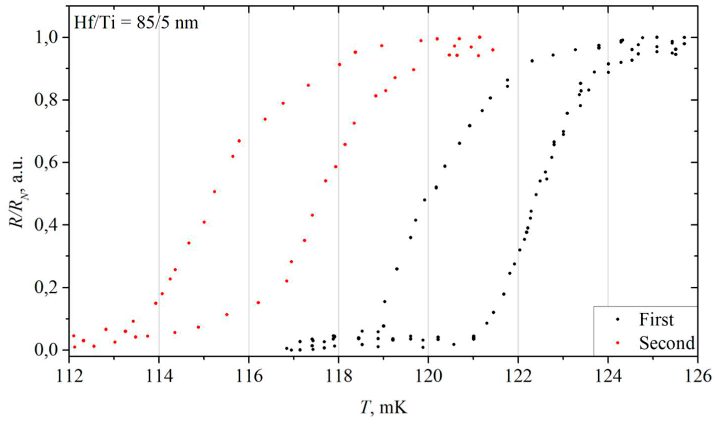
Figure 13). R(T) for this time was very similar to R(T) measured previously. The transition was from 115 mK till 120 mK. On cooling the resistance decreased to zero from 118 mK to 113 mK. Thus this film almost maintained all characteristics during two months.
The changes are very minor compared to some other films’ repeated measurements. One can see that the critical temperature of the film only slightly decreased (
Figure 10, red dots), and the other properties did not change. This signals that the top layer made of very thin titanium film protects hafnium from oxidation and other processes over time.
This preservation can also be explained by peculiar properties of titanium oxide film, which is formed on the entire surface of the sample, and it is very hard to damage it under some random circumstances. Therefore, the investigations of hafnium films with titanium top layers will be continued.
3.5.5. Hf New 100 nm on Si
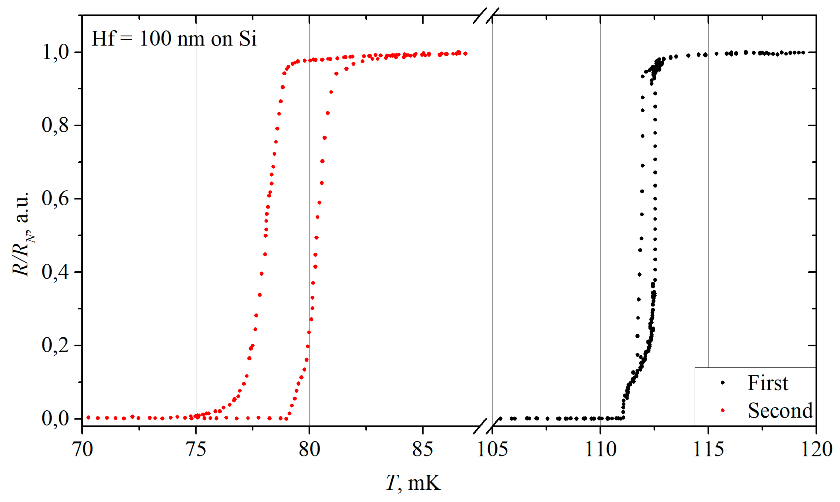
The measurements were repeated for Hf film 100 nm thick on silicon substrate. The IV curve had the same shape, but the critical current fell from 4.4 μA to 2.9 μA, while normal resistance remained the same 7.8 Ohm. Then R(T) was measured (
Figure 14).
In this measurement the film resistance started to increase at 78 mK, and the film turned to normal state at 83 mK. On cooling the resistance fell down in the (78-75) mK range. This divergence increase between heating and cooling can be explained by higher film overheating in normal state despite very low measuring current.
These results differ significantly from the first measurements of this film, both the critical current and the critical temperature (
Figure 10, red dots) decreased by more than 30%. The exact reasons for such changes in these characteristics are yet to be determined.
4. The Possible Reasons for Changes in the Critical Temperature of Hf Films
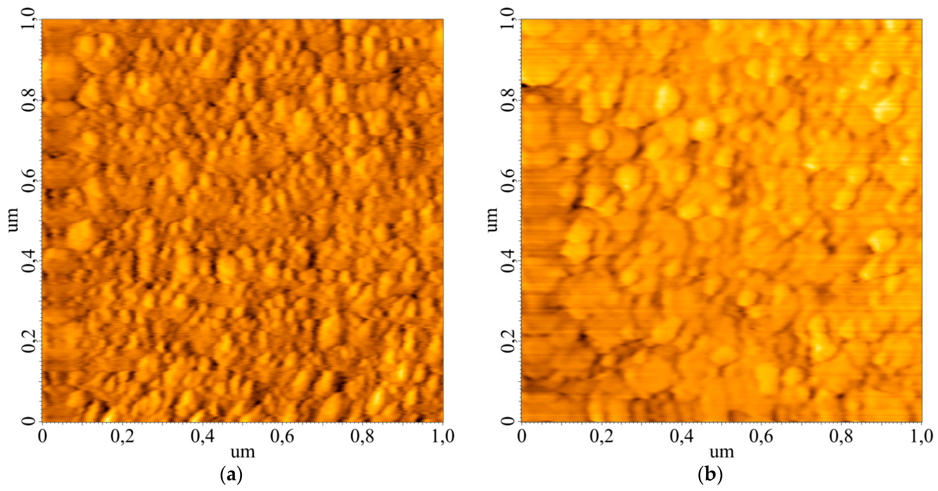
Our data suggest that the variation of the critical temperature of the films over time may happen due to different reasons for a single layer Hf and for Hf with normal metal layers. Different mechanisms for changing the transition temperature also follow from AFM images taken on pure hafnium and hafnium coated with silver (
Figure 15).
The film of 100 nm “new” Hf was studied on Si [100] substrate using an atomic force microscope (AFM), right after the deposition. AFM image of the surface is shown in
Figure 15a. The surface looks rather smooth with randomly distributed grains. The average lateral size of the grains is several tens of nm.
Figure 15b shows an AFM image of a hafnium film covered by silver with thicknesses of 85 and 30 nm, respectively. In contrast to the “fresh” Hf film, shown in
Figure 15a, this Hf/Ag film was analyzed after several measurements in the fridge. It is clearly visible that the silver coating has changed the structure of the surface. An obvious cluster structure is visible. The lateral sizes of the clusters are noticeably larger than the sizes of the granules in
Figure 15a.
For a single hafnium we suggested that the properties may drift due to a change in the effective thickness of the hafnium film due to the growth of a HfO2 layer on the film surface. According to data from the Bruker diffractometer, the thickness of the oxide in the atmosphere grows to 2.6 nm over a month and then remains virtually unchanged.
As for the films with layers of normal metals there is another hypothesis that the change in the critical temperature may be associated with the recrystallization of the film over time due to thermal cycling. In this case, larger crystallites can form in a film after cooling and warming. We examined several Hf/Ag films with different thicknesses of silver from 10 to 30 nm on AFM and the surfaces look similar for all investigated silver thicknesses. It is known that silver has a great ability to diffuse into other metals. In our case, this can create defects in the hafnium crystal lattice, which in turn contributes to the formation of crystallization centers. Over a short period of time, this leads to the formation of larger crystallites, leading to relaxation of the film, changing its superconducting properties. Also this hypothesis can be confirmed by the observation of Ref. [
16] that hafnium films with larger crystallites have larger critical temperature.
We also investigated the roughness of hafnium films. First, a Talysurf 2000 white light interferometer was used, the results showed an RMS roughness of 1.67 nm in a field of 0.5x0.6 mm for a 60 nm film (using a Talysurf data). Second, data from an X-ray diffractometer showed a roughness of 1 nm for this film, while the actual film thickness was 57 nm. We have found that a quartz sensor in the vacuum chamber of an e-beam evaporator systematically showed smaller thicknesses of deposited hafnium films than actual values determined by Talysurf or X-ray diffractometer. Such a difference in thickness may indicate that the film creates stress on the quartz sensor, which increases the sensor error. Therefore, we can presume that the stressed film would relax over time, including changes in its crystal structure.
More characteristic changes in the crystal structure of films can be determined by TEM analysis. In the future, it is planned to conduct a series of experiments with artificial aging of films, with analysis using available equipment, including TEM.
5. Conclusion
Hafnium metal has very convenient properties for low temperature applications, namely, a critical temperature close to 100 mK and a narrow width of the superconducting transition, required for the development of a TES detector.
We have shown that e-beam deposition of hafnium allows obtaining superconducting films of thickness about 100 nm and with roughness just 1-2 nm. These results are in agreement with literature data.
We have managed to decrease the critical temperature of hafnium films, deposited on substrate by electron beam evaporation method, below 100 mK, keeping the transition widths within a few millikelvin. The suppression of the critical temperature is realized by using the proximity effect with layers of normal metals such as silver and gold.
We have observed the instability of transition temperatures in some films. In single layer Hf films the critical temperature tends to decrease with time while in bi- and three-layer samples with normal metals (silver and gold) the transition temperature significantly increases. In the latter case the critical temperature for some of the films increased twofold since the first measurement. It can be explained by recrystallization caused by silver after thermal cycling.
We have proposed and tested a solution of how to preserve superconducting properties of hafnium films from changing. For this we have used thin titanium top layers with thickness of about 5 nm. The layer with this thickness is enough to keep the critical temperature and critical current of the film stable in the course of time and after thermocycling. The combination of hafnium and titanium films appears to be promising for further development of a TES microcalorimeter based on hafnium films.
Author Contributions
Conceptualization, A.V.G.; methodology, A.V.G., A.L.P. and V.Y.S.; software, D.A.P. and A.A.Y.; validation, A.V.G., A.L.P. and V.Y.S.; formal analysis, A.V.G.; investigation, V.Y.S.; resources, A.V.B., V.Y.S and O.L.E.; data curation, A.V.G., A.L.P. and V.Y.S.; writing—original draft preparation, V.Y.S. and D.A.P.; writing—review and editing, A.L.P., A.V.G. and V.Y.S.; visualization, V.Y.S. and A.V.G.; supervision, A.V.G. and A.L.P.; project administration, A.V.G.; funding acquisition, A.V.G. All authors have read and agreed to the published version of the manuscript.
Funding
This study was conducted within the scientific program of the National Center for Physics and Mathematics, section #8. Stage 2023-2025.
Institutional Review Board Statement
Not applicable.
Informed Consent Statement
Not applicable.
Data Availability Statement
The data that support the findings of this work are available from the corresponding author upon reasonable request.
Acknowledgments
The facilities of the Center of Quantum Technologies of NNSTU and Common Research Center “Physics and technology of micro- and nanostructures” of IPM RAS were used.
Conflicts of Interest
The authors declare no conflict of interest. The funders had no role in the design of the study; in the collection, analyses, or interpretation of data; in the writing of the manuscript; or in the decision to publish the results.
References
- Ullom, J.N.; Bennett, D.A. Review of superconducting transition-edge sensors for x-ray and gamma-ray spectroscopy. Supercond. Sci. Technol. 2015, 28, 084003. [Google Scholar]
- Kunieda, Y.; Fukuda, D.; Ohno, M.; Takahashi, H.; Ataka, M.; Ohkubo, M.; Hirayama, F.; Nakazawa, M. Development of Ir/Au-TES Microcalorimeter. J. Nucl. Sci. Technol. 2004, 41(4), 144–147. [Google Scholar]
- Lita, A.E.; Calkins, B.; Pellochoud, L.A.; Miller, A.J.; Nam, S. High-Efficiency Photon-Number-Resolving Detectors based on Hafnium Transition-Edge Sensors. AIP Conference Proceedings, 16 December 2009, 1185(1), 351–354. 16 December.
- Merenkov, A.V.; Shitov, S.V.; Chichkov, V.I.; et al. A Superconducting Resonator with a Hafnium Microbridge at Temperatures of 50–350 mK. Tech. Phys. Lett. 2018, 44, 581–584. [Google Scholar] [CrossRef]
- Lubsanov, V.; et al. Materials for a broadband microwave superconducting single photon detector. Supercond. Sci. Technol. 2022, 35, 105013. [Google Scholar] [CrossRef]
- Zhang, H.; et al. The potential and challenges of time-resolved single-photon detection based on current-carrying superconducting nanowires. J. Phys. D: Appl. Phys. 2020, 53, 013001. [Google Scholar] [CrossRef]
- Kim, S.H.; Jeong, H.S.; Kiuchi, K.; et al. Development of Superconducting Tunnel Junction Photon Detector using Hafnium. Phys. Procedia 2012, 37, 667–674. [Google Scholar] [CrossRef]
- Kraft, S.; Peacock, A.J.; Bavdaz, M.; Castelletto, B.; Collaudin, B.; Perez, D.; Venn, R.; Harper, T.E. Use of hafnium-based superconducting tunnel junctions as high-resolution spectrometers for x-ray astronomy. In EUV, X-Ray, and Gamma-Ray Instrumentation for Astronomy IX. Proc. SPIE, 10 November 1998, 3445, 226–235.
- Hunacek, J.; Bock, J.; Bradford, C.M.; et al. Hafnium Films and Magnetic Shielding for TIME, A mm-Wavelength Spectrometer Array. J. Low Temp. Phys. 2018, 193, 893–900. [Google Scholar] [CrossRef]
- Bogorin, D.F.; Galeazzi, M. Characterization of Iridium Thin Films for TES Microcalorimeters. J. Low Temp. Phys. 2008, 151, 167–172. [Google Scholar] [CrossRef]
- Kunieda, Y.; et al. Comparison of Superconducting Transition Characteristics of Two Iridium/Gold Bilayer Transition Edge Sensor Devices. Jpn. J. Appl. Phys. 2004, 43, 2742. [Google Scholar] [CrossRef]
- Mitsuya, Y.; Konno, T.; Takasu, S.; et al. Photon Number Resolution with an Iridium Optical Transition Edge Sensor at a Telecommunication Wavelength. J. Low Temp. Phys. 2023, 210, 498–505. [Google Scholar] [CrossRef]
- Nagel, U.; Nowak, A.; Kellner, E.; et al. Use of Proximity Effect in Iridium-Gold Superconducting Phase Transition Thermometers. J. Low Temp. Phys. 1993, 93, 543–548. [Google Scholar] [CrossRef]
- Hennings-Yeomans, R.; Chang, C.L.; Ding, J.; et al. Controlling Tc of iridium films using the proximity effect. J. Appl. Phys. 2020, 128(15), 154501. [Google Scholar] [CrossRef]
- Lita, A.E.; et al. Tuning of tungsten thin film superconducting transition temperature for fabrication of photon number resolving detectors. IEEE Trans. Appl. Supercond. 2005, 15(2), 3528–3531. [Google Scholar] [CrossRef]
- Mardare, A.; Siket, C.; Gavrilovic-Wohlmuther, A.; Kleber, C.; Bauer, S.; Hassel, A.W. Anodization Behavior of Glassy Metallic Hafnium Thin Films. J. Electrochem. Soc. 2015, 162, E30–E36. [Google Scholar] [CrossRef]
- Keast, V.J. Atmospheric Corrosion of Silver and Silver Nanoparticles. Corros. Mater. Degrad. 2022, 3, 221–234. [Google Scholar] [CrossRef]
|
Disclaimer/Publisher’s Note: The statements, opinions and data contained in all publications are solely those of the individual author(s) and contributor(s) and not of MDPI and/or the editor(s). MDPI and/or the editor(s) disclaim responsibility for any injury to people or property resulting from any ideas, methods, instructions or products referred to in the content. |
© 2023 by the authors. Licensee MDPI, Basel, Switzerland. This article is an open access article distributed under the terms and conditions of the Creative Commons Attribution (CC BY) license (http://creativecommons.org/licenses/by/4.0/).
