Preprint
Article

Power Receiving Unit for High Power Resonant Wireless Power Transfer

Altmetrics

Downloads

88

Views

29

Comments

0

A peer-reviewed article of this preprint also exists.

Submitted:

23 October 2023

Posted:

23 October 2023

You are already at the latest version

Alerts
Abstract
A new power receiving unit (PRU) is proposed in this paper for the resonant wireless power transfer (WPT), which is characterized by the capability of attracting high power from the power transmitting unit (PTU). The resonant WPT is designed for delivering the electrical power to the PRU attached on an electrical vehicle (EV) chassis 50cm away from a PTU installed on the ground. The proposed PRU uses only the passive elements such as inductors, diodes and the capacitors, which needs no initial power from the EV. It is then applicable for charging a battery to several hundred volts for even a first-time charging battery. At a switching frequency of the resonant WPT in the experiment being 4MHz, the proposed PRU behaves itself as a negative impedance converter (NIC) in the subharmonics of 4MHz. The NIC effect plus the subharmonic oscillation causes an instability current charging the battery connected to the PRU. In this paper, we simulated the PRU and performed the experiment. The experiment demonstrates a battery charging of 150W from 50cm away using three D-mode GaN HEMT transistors via the instability current ramp. The power transfer efficiency (PTE) improved as the power delivered to load (PDL) goes higher. The best power transfer efficiency (PTE) is 65% in the present findings. The simulation analysis shows that the circuit allows itself be used to much higher power transfer when it is implemented with more GaN HEMT transistors connected in parallel. The theoretical derivation of the PRU circuit is also used to support both the experimental and simulation results.
Keywords: 
Subject: Engineering  -   Mechanical Engineering

1. Introduction

Wireless power transfer (WPT) technologies are becoming promising in various application areas due to the crucial problems of range anxiety and bulky battery [1,2]. The wide bandgap semiconductor devices, such as GaN HEMTs and SiC, boost the performance of wireless power applications due to their unique material characteristic: low capacitance and high switching [3,4]. Most of the results have shown that using WBG devices as switching devices, results in higher transfer efficiency and density [5,6].
Among WPT technique, resonant WPT has attracted more attention, because it can not only require serious precise coil alignment and tight coupling but also extend the power transfer range. Namely, the resonant WPT has excellent endurance on the position offset and angular misalignment between the transmitting and receiving coils [7,8]. However, the resonance mechanism for high wireless power transfer required an extremely low resistance coil for long distance [9], which is hardly achievable in practice when the copper has non-zero resistance until the resonance frequency reaches 20 kHz.
Therefore, the negative impedance converter (NIC) was proposed to generate negative resistance for reducing the resistance of the coil [10]. Some study has shown the power transmission efficiency was improved at a long distance with the NIC [11]. Moreover, using negative impedance converter can also maximize the system efficiency [12]. Besides, the output electricity should be regulated no matter how varied it becomes. Previous works have investigated several power-regulation methods, which can be classified into three types: 1) passive regulation, 2) active rectification, and 3) post-stage regulation (by LDO or DC-DC) [13,14]. Some literatures, such as hybrid multi-level buck post-regulator has been exploited for improving spatial freedom [13].
Basically subharmonic oscillation [15,16] is not a small signal instability, it's a large signal phenomenon in peak current mode control that occurs when the duty cycle is greater than 50% typically, under certain circumstances it can occur below 50% duty cycle as well. By adding a ramp signal to the output of the error amp it is possible to stabilize a peak current mode converter for all duty cycles, but the control loop no longer behaves exactly like a current mode converter [15].
In this study, we proposed a PRU topology, which behave as NIC effect as well as the subharmonic oscillation causes an instability current for charging the battery. First, the main components of resonant WPT including PTU, PRU, Transformer model, GaN HEMT module, and subharmonic oscillation, are introduced in section 2. Then, the PRU module comprising AC-DC converter circuit and resonant capacitive voltage divider output load was presented to achieve battery charging. Moreover, flat-band band-pass filter and magnetic coupling coefficient are also discussed in section 3. Finally, the experimental and simulation results are presented to support the theoretical derivation of the PRU circuit.

2. GaN HEMT Based Class E Resonant Wireless Power Transfer

2.1. Power Transmitting Unit (PTU)

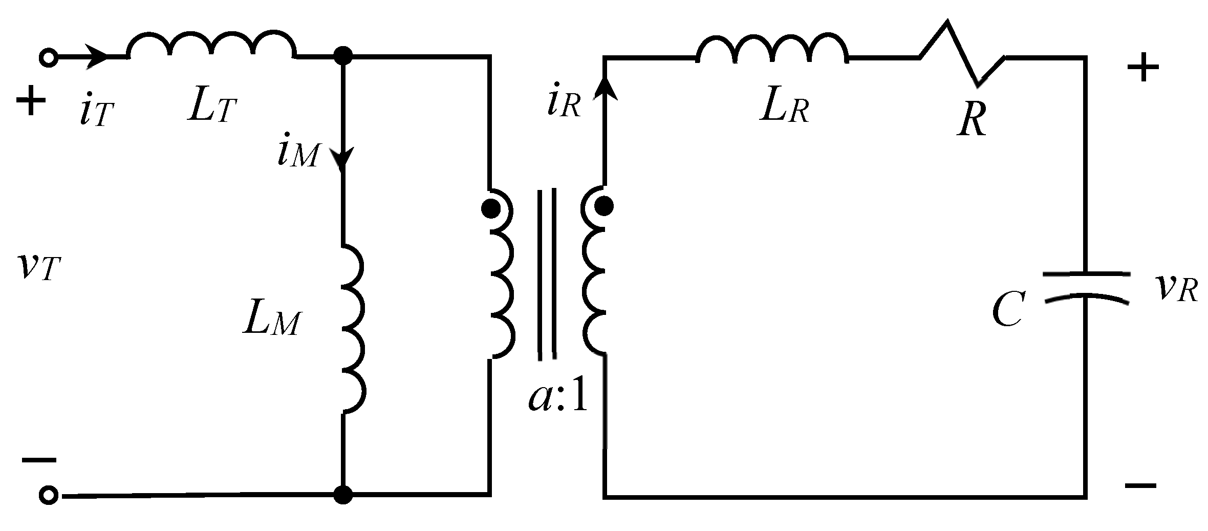
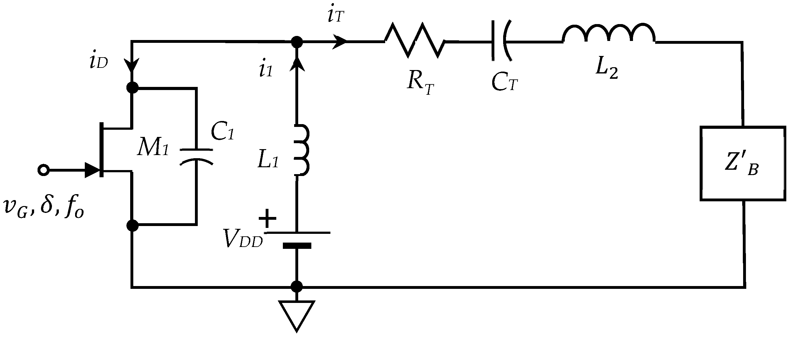
Since the wireless power transfer does not have a magnetic core, the equivalent circuit of the wireless transformer can be obtained by removing the core-loss resistance which was in parallel with the magnetization inductance Lm from the general version of transformer, the Steinmetz equivalent circuit, and shown in Figure 1.
d i 1 d t = V D D v x ( t ) L 1
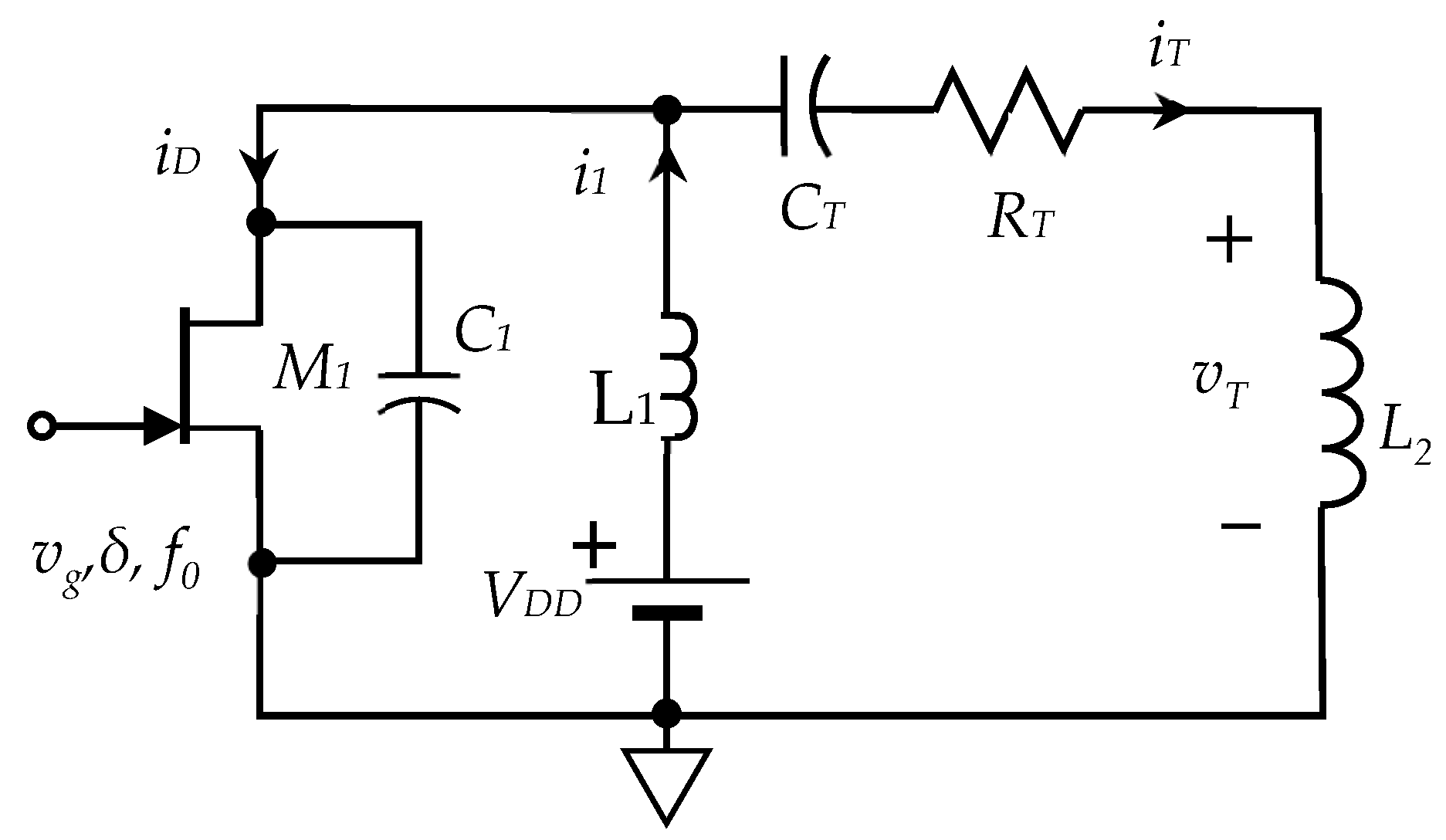
The increased current i 1 converted the electrical energy from the DC source V D D to the energy in the magnetic field using the electrical current. The magnetic energy is then transferred to the impedance load side when the switch M 1 turns off. Therefore, the power delivered to load (PDL) is proportional to the amount of the magnetic energy absorbed into the inductor which is a function of the current i 1 increment. For achieving higher PDL, we need to obtain the lowest v x ( t ) possible at the instance when the switch M 1 turns on and the switch M 1 turns off when v x ( t ) rises back to V D D . The resistance R T denoting the coil resistance is preferred to be as small as possible to increase the power efficiency during wireless power transfer.
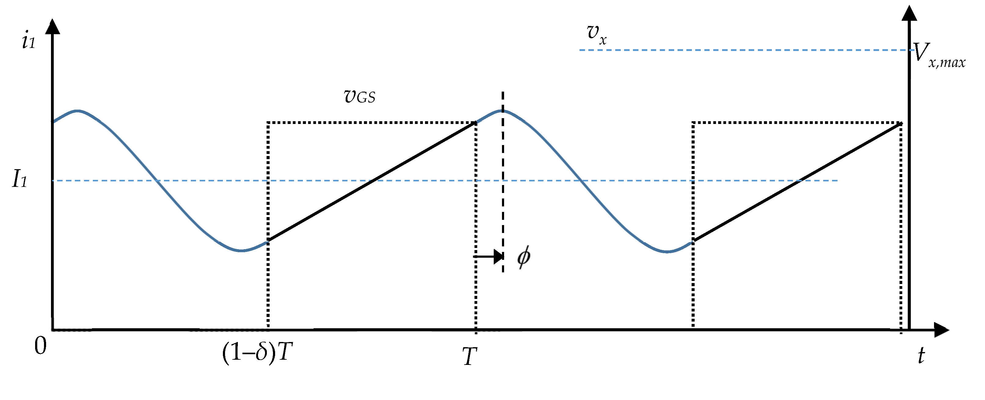
It was derived in [17] that the maximum value of the nodal voltage is a function of the current phase angle ϕ , as shown in Figure 2, as follows.
V x , m a x = V D D ( 1 + 1 c o s ϕ )
where t a n ϕ π ϕ = δ 1 δ
The above equation is valid only for the ZVS control of the switch M 1 in steady state response, which may not hold for the transition states. The corresponding current phase angle ϕ is 64 0 and the corresponding voltage magnification V x , m a x / V D D is 3.28 at steady state [1].

2.2. Power Receiving Unit (PRU)

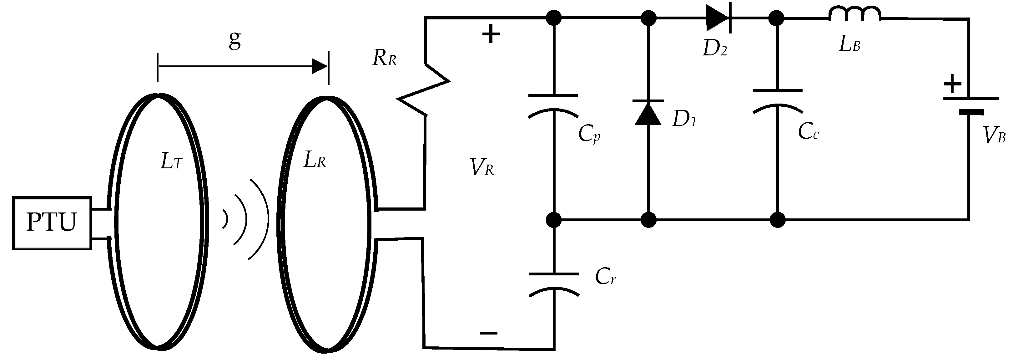
A specific kind of PRU is proposed in this paper, as shown in Figure 3. The impedance load is connected via the magnetic linkage between the PTU and the PRU. The receiving voltage swing on the PRU side is a function of the distance from the PTU coil and the condition of resonance determined by the PRU capacitance.
v R = v R ( f 0 , g , C R )
The receiving voltage amplitude on the PRU coil is a function of distance g away from the PTU coil and the condition of the resonance to the signal switching frequency f 0 . Among these parameters, the wireless signal switching frequency f 0 is determined by the PTU which has to provide service to multiple users. The distance g of the specific PRU away from the PTU is a degree of freedom for the user. The PRU is allowed only to adjust the capacitance C R to achieve the best power transfer condition referred to as the minimum power input control.

2.3. Transformer Model for WPT

The parallel quality factor Q_P is defined as follows.
Q P = R R C R L R
When the PTU and PRU are with similar windings, i.e. L T = L R , the magnitude voltage gain G v , 1 is derived under the perfect resonance matching condition, i.e. the switching frequency 2 π f 0 = 1 / L R C R as follows [9].
G v , 1 = V R V T = k k 2 + j Q P
The above equation had ignored both effects of the magnetization current flowing through L M   and the coil loss through the coil resistance R T . k denotes the coupling coefficient between the transmitting and receiving winding coils. The coupling coefficient k is larger than Q P when the distance between the coils are small and is much smaller than Q P in the long distance WPT. The magnitude and the phase of the voltage gain are expressed individually as follows.
| G v , 1 | = k k 4 + Q P 2 G v , 1 = t a n 1 Q P k = { 0 o p u r e   i n d u c t i v e   W P T 90 o p u r e   R e s o n a n t   W P T
The resulting equivalent circuit for the resonant wireless power transfer is equivalent to the class-E circuit as shown in Figure 5. The resonance WPT transformer circuit model shown in Figure 4 acts as an impedance inverter that invert the capacitor C R into an inductor L 2 . The equivalent impedance L 2 mapped from the PRU to the PTU is derived as follow.
j ω 0 L 2 = 1 G v , 1 2 1 j ω 0 C R
where ω0=2πf0
The above equation is analogous to the transformer of turn ratio 1 : G v , 1 . Due to the turn ratio is a complex number, hence the capacitor became a negative capacitor which is equivalent to an inductor with the inductance derived as follows.
L 2 = Q p 2 k 2 1 ω 0 2 C R = R R 2 k 2 C R
We let the undamped natural frequency of PTU be denoted by ω 2 as follows.
ω 2 = 1 L 2 C T = k R R 1 C R C T

2.4. GaN HEMT Module

The study employed a D-mode GaN HEMT, which was manufactured at the Compound Semiconductor Laboratory, National Yang-Ming Chiao-Tung University, Taiwan. This device boasts a total gate width of 20 mm, offering a current density of 500 mA/mm and an on-resistance of 50 mΩ/mm. Notably, it possesses a breakdown voltage of 600 V and a gate threshold voltage of −9V. The accompanying parasitic capacitances and other pertinent characteristics are comprehensively outlined in Table 1.
To address packaging concerns, the 20 mm D-Mode GaN HEMT is encased in a Transistor Outline 220 (TO220). While the Dual Flat No-Lead (DFN) package which can effectively minimize the impact of stray inductance, the TO220 packaging exhibits a better thermal resistance. The reduction in the width of the GaN HEMT device represents a significant improvement over our previous version, which had a total gate width of 120 mm and was encapsulated in a TO220 package. The 20 mm D-mode GaN HEMT presents a six times smaller parasitic capacitance compared to 120 mm version. The utilization of the 20 mm D-mode GaN is particularly advantageous for high-frequency operations within the MHz range, rendering it an optimal choice for resonant wireless power transfer.

2.5. Subharmonic Oscillation

Subharmonic oscillations, whose frequency is a fraction 1/ n (n= 2, 3, 4, ...) of that of the applied force term, may frequently occur in nonlinear systems [18], which were found in both theoretical results and experiments conducted for an electrical oscillatory circuit containing a saturable iron-core inductance and a capacitance. The PRU proposed in this paper used the diodes whose current output is nonlinear with respect to the input voltage across the diodes. The diodes turn on and off in accordance with not only the voltage but also the current itself in a practical model of the high frequency, high voltage SiC diode. The nonlinear differential equation can produce the subharmonic responses whose frequency is a fraction of the input, fixed frequency. The individual terms in the nonlinear differential equation must include the instantaneous states of voltage and current. In our experiments, the subharmonic response occurs when the DC supply voltage V D D on the PTU site is higher than some voltage level when the voltage-gain between the PRU coil and PTU coil is higher than the conducting threshold voltage of the diodes in the PRU. In this paper, we can only show the existence of subharmonic responses instead of providing complete theoretical results as the comparison.

3. PRU Module for Battery Charging

3.1. AC-DC Converter

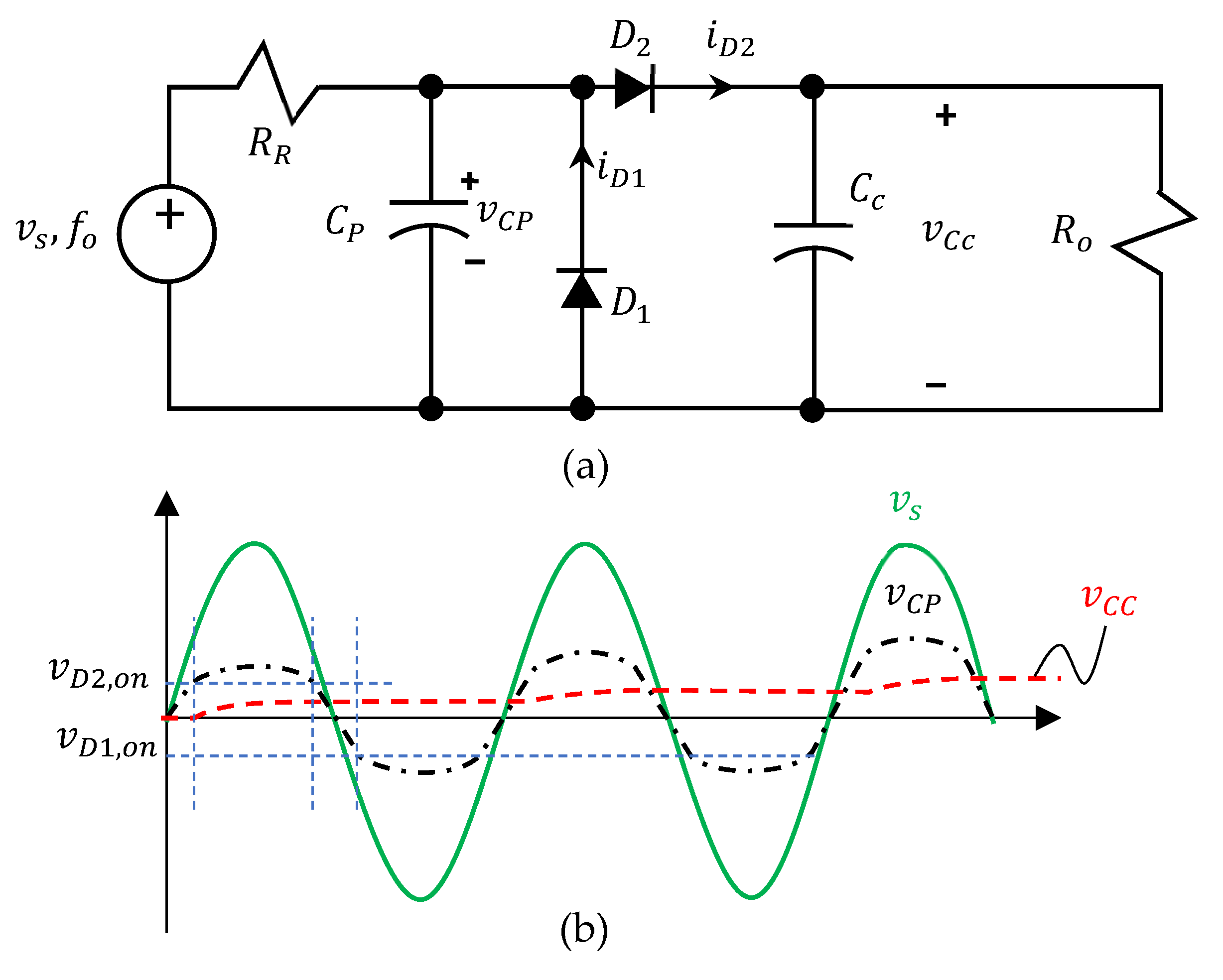
A AC-DC converter circuit using diode rectifier is shown in Figure 6, which has the advantage on converting the high voltage AC source into a low voltage DC storage. The diode D 1 is used to prevent the negative charging into the capacitor C P . The diode D 2 works together with the capacitor C c is the peak detector circuit. The two diodes turn on alternatively to limit the voltage in the capacitor C P , thus the capacitor voltage on C P is derived for low current as follows.
V D 1 , o n v C P v D 2 , o n + V C c , m i n
The charging time of the capacitor C P must be smaller than the period time of the input source V s , however the smaller the resistance of R R is, the larger the resistive loss of the converter is when the voltage goes to negative cycle. It is in practice that the high frequency diode resistance is 0.2 Ohm, thus the capacitor voltage v C P can be increased by the actual voltage across the diodes as follows.
( V D 1 , o n + I D 1 , m a x R D 1 , o n ) v C P V D 2 , o n + I D 2 , m a x R D 2 , o n + V C c , m i n
The peak detector capacitor voltage v C C is a function of charging through the resistor R R up to V s V D 2 , o n and discharging from the load R o . Assuming the R R is very small, we then have the steady state result of the minimum value of capacitor voltage C C c , m i n as follows.
V C c , m i n = ( V s V D 2 , o n ) 1 e 1 / ( 2 f 0 R R C c ) e 1 / ( 2 f 0 R o C c ) e 1 / ( 2 f 0 R R C c ) ( V s v D 2 , o n ) e 1 2 f 0 R 0 C c
The maximum current of diode D 1 and D 2 respectively may be obtained as follows.
I D 1 , m a x = V s V D 1 , o n R R I D 2 , m a x = V s V D 2 , o n V C c , m i n R R
Subjected to heavy load R o , the two diodes have the same maximum current, i.e. I D 1 , m a x I D 2 , m a x .

3.2. Resonant Capacitive Voltage Divider

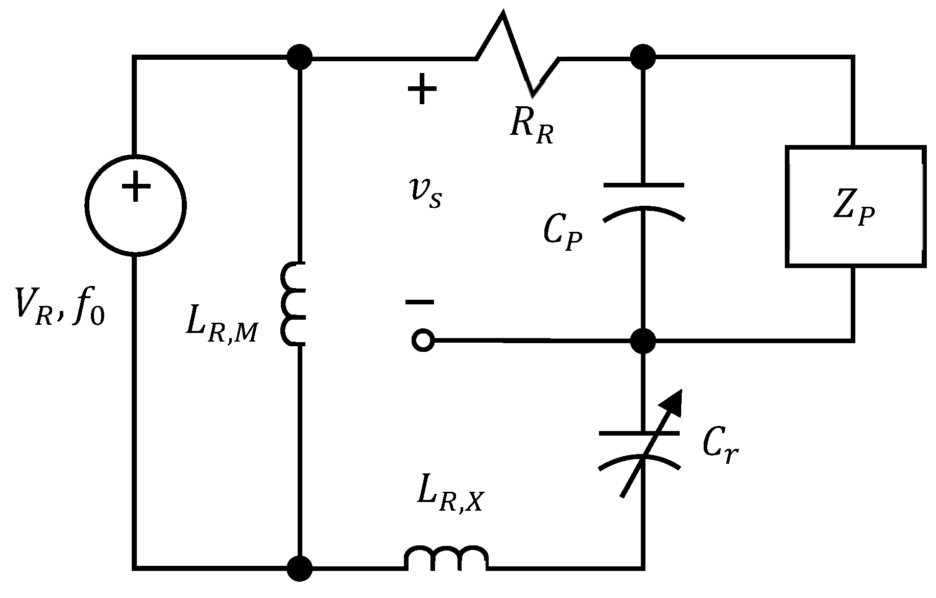
The input source to the AC-DC converter is a resonant capacitive voltage divider which is modeled as shown in Figure 7. The capacitor C R is adjustable to tune the series resonance between itself and the processing capacitor C P with the inductor L R . It is assumed that a very small part of the inductor L R acts as the magnetization inductor L R , M as a secondary coil of the transformer and the rest of the inductance L R , X into the leakage inductor. The resonant voltage is typically higher than hundreds of watts. For achieving the voltage reduction as well as maintain the resonance phenomenon, the capacitor   C P inserted in series with the resonance capacitor C r in the LC tank integrates a new total capacitance.
C R = C r C P C r + C P
The voltage resonance occurs when the resonant frequency of the series LC tank f L C matches the input frequency f o providing the leakage inductance is much larger than the magnetization inductance, i.e. L R L R , X , as follows.
V s = C r C r + C P V R
The voltage resonance occurs when the resonant frequency of the series LC tank f L C matches the input frequency f o providing the leakage inductance is much larger than the magnetization inductance, i.e. L R L R , X , as follows.
f 0 = f L C = 1 2 π L R , R C R 1 2 π L R C R
Adjusting the capacitance of C r which subsequently changes C R , we can tune the resonant frequency of the series LC tank with the equation as follows.
Δ f L C = 1 4 π ( L R C R ) 3 2 L R C R C r Δ C r = C R 2 f L C C r 2 Δ C r
Since the exact f L C is unknown when doing the adjustment however the transmitting frequency f 0 is known, the following equation may be used in the tuning providing that C P >> C r .
Δ f L C f 0 = K f Δ C r C r
where K f = C P 2 C r
The above equation is stated as the percentage change of the capacitance is proportional to the ratio of C P and C r . To allow a low sensitivity of capacitance adjustment which is preferable to the fine tune, the capacitance of C P shall be reduced. But on the other hand, the voltage does into the load is also increased to a very high voltage which is unfavorable to the heavy load Z P application that can take too much charge from the resonance LC tank and break the resonance mechanism.

3.3. Battery Charger Using a Flat-band Band-Pass Filter

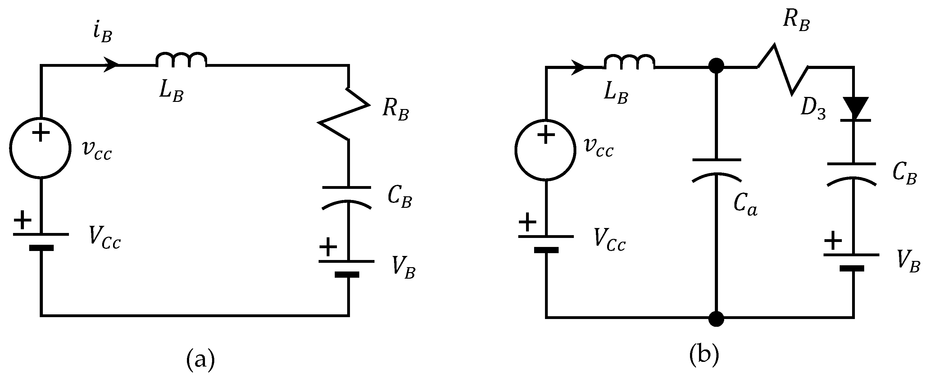
The output load of the AC-DC converter is a resonant capacitive voltage divider which is modeled as shown in Figure 8(a). The battery may be modeled using a resistor R B representing the electrodes and interlayer connection loss, a capacitor C B representing the instantaneous capacitive behavior for charge storage, and an ideal DC voltage source V B . The resistor R B is temperature dependent, which is typically around 0.1 Ω in room temperature for the Lithium-ion battery. The capacitor C B are typically thousands of Faraday each individual Lithium-ion battery. The input source of the battery charger is a DC voltage source v C c superimposed with an AC voltage source v C c . For reducing the energy loss of the low-pass filter, aside from a small resistance resistor R B we used an inductor to serve as a choke to absorb the voltage difference between the input voltage and the battery DC voltage V B . The governing equation for the current to charge the battery capacitor C B of the circuit in Figure 8(a) is formulated as follows.
L B d i B d t + R B i B + i B d t = v c c + ( V C c V B )
Providing the assumption of steady state when V B = V C c , we derived the Laplace transform between the AC voltage v c c and the output current i B as follows.
I B ( s ) V C C ( s ) = s L B s 2 + R B s + 1 C B
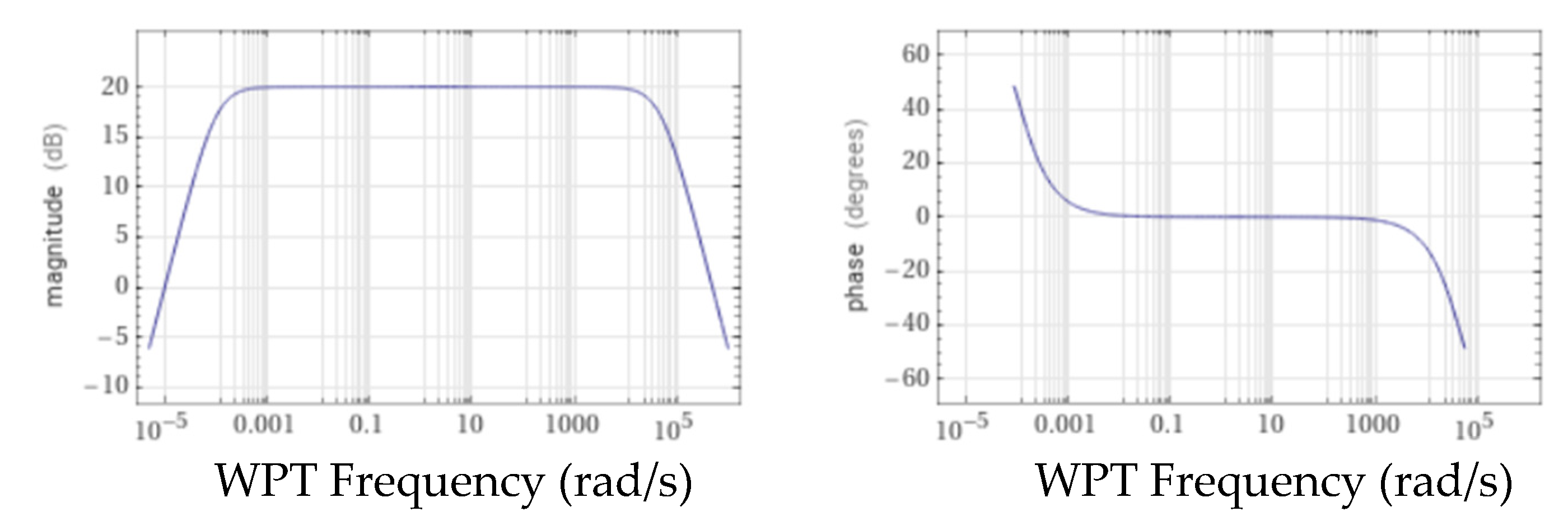
For the specific frequency f 0 of wireless power transfer in the range between 4 to 15 MHz, one may choose L B in uH which together with the large capacitance of C B and the zero at the origin form a flat-band band-pass filter that has low voltage gain on the high frequency component and has also low voltage gain on the ultra-low frequency component, i.e. the difference voltage between V B and V C c , to prevent the current surge from the battery during the initial charging. The alternative circuit to expedite the current surge from the battery during the connection of the battery to the circuit is to add a stabilization capacitor C a along with a diode as shown in Figure 8 (b). We can use a diode to protect the reverse current flow from the battery to the inductor L B or even the high frequency stabilization capacitor C a   on the AC-DC converter. Figure 9 demonstrates the Bode plot for the band-pass filter with L B = 2 uH, C B = 10,000 F and R B = 0.1 Ohm.
The equivalent impedance of battery charger is derived as follows when assuming that the AC-DC conversion is at its steady state.
Z B = V s I B
Using the same parameters L B = 2 uH, C B = 10,000 F and R B = 0.1 Ohm, we calculate the equivalent loading is a resistance 0.1 Ohm with zero phase in a frequency band between mHz to 10kHz. The resulting equivalent circuit for the resonant WPT subjected to PRU is shown in Figure 10.
R = ρ l w A
The above equation shows a negative resistance which may cancel out the resistance R T   from the PTU and even induce instability of the wireless power transfer. At the steady state of resonance, the PRU circuit is a negative impedance converter (NIC) which converts the positive resistance into a negative resistance within the bandwidth between sub-Hz to 30 kHz. For the resonant frequency component of the input signal, the PRU circuit converts the instantaneous capacitance of the battery into the inductance L 2 as indicated in Figure 10. When the absolute value of the negative resistance of the impedance Z B is much higher than that of the PTU coil resistance, the LC tank in the PRU becomes associated with a negative damping which can cause the instability of the circuit response. Therefore, we will need a closed loop current control to stabilize the circuit in the future.

3.4. Magnetic Coupling Coefficient

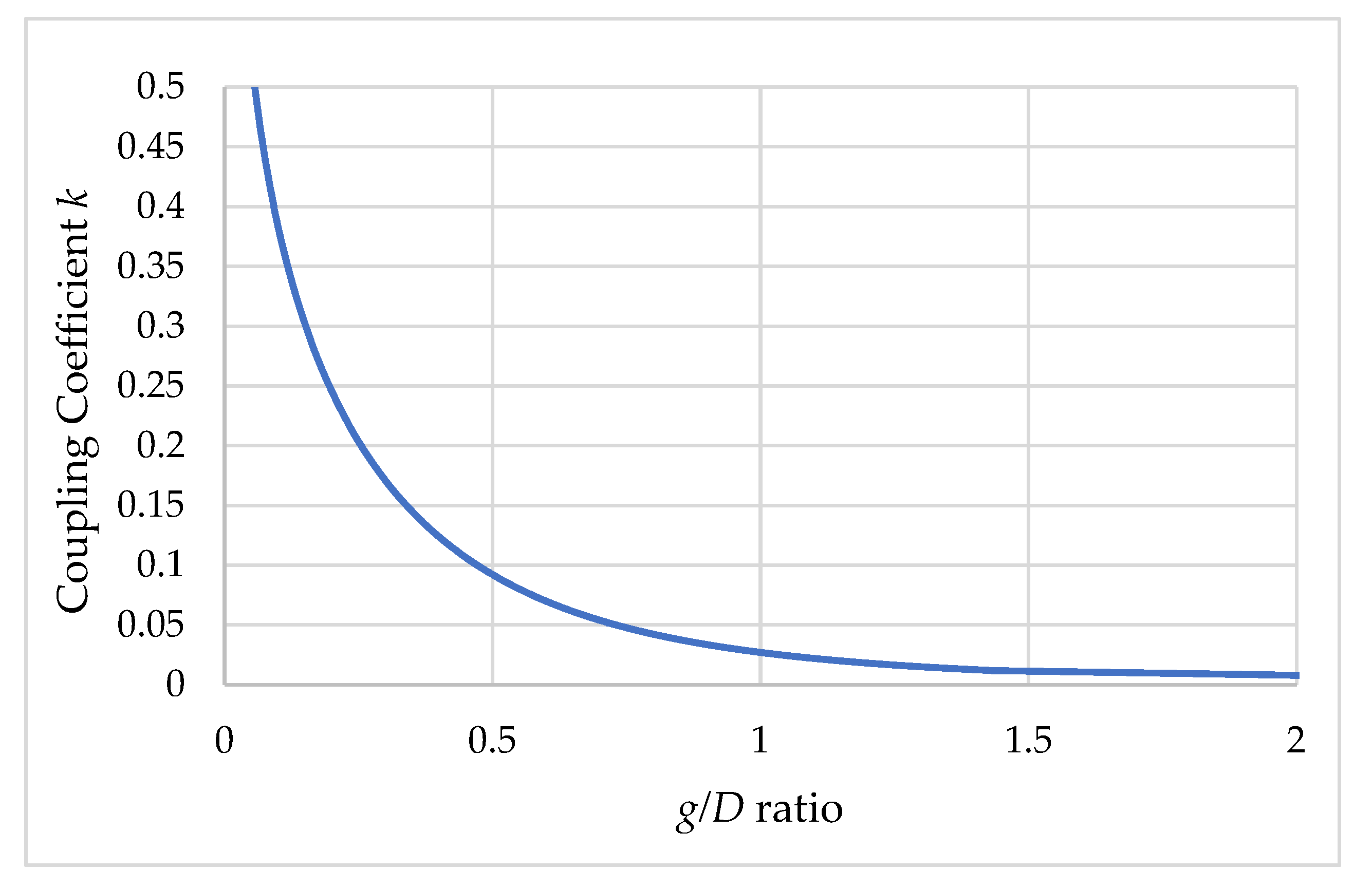
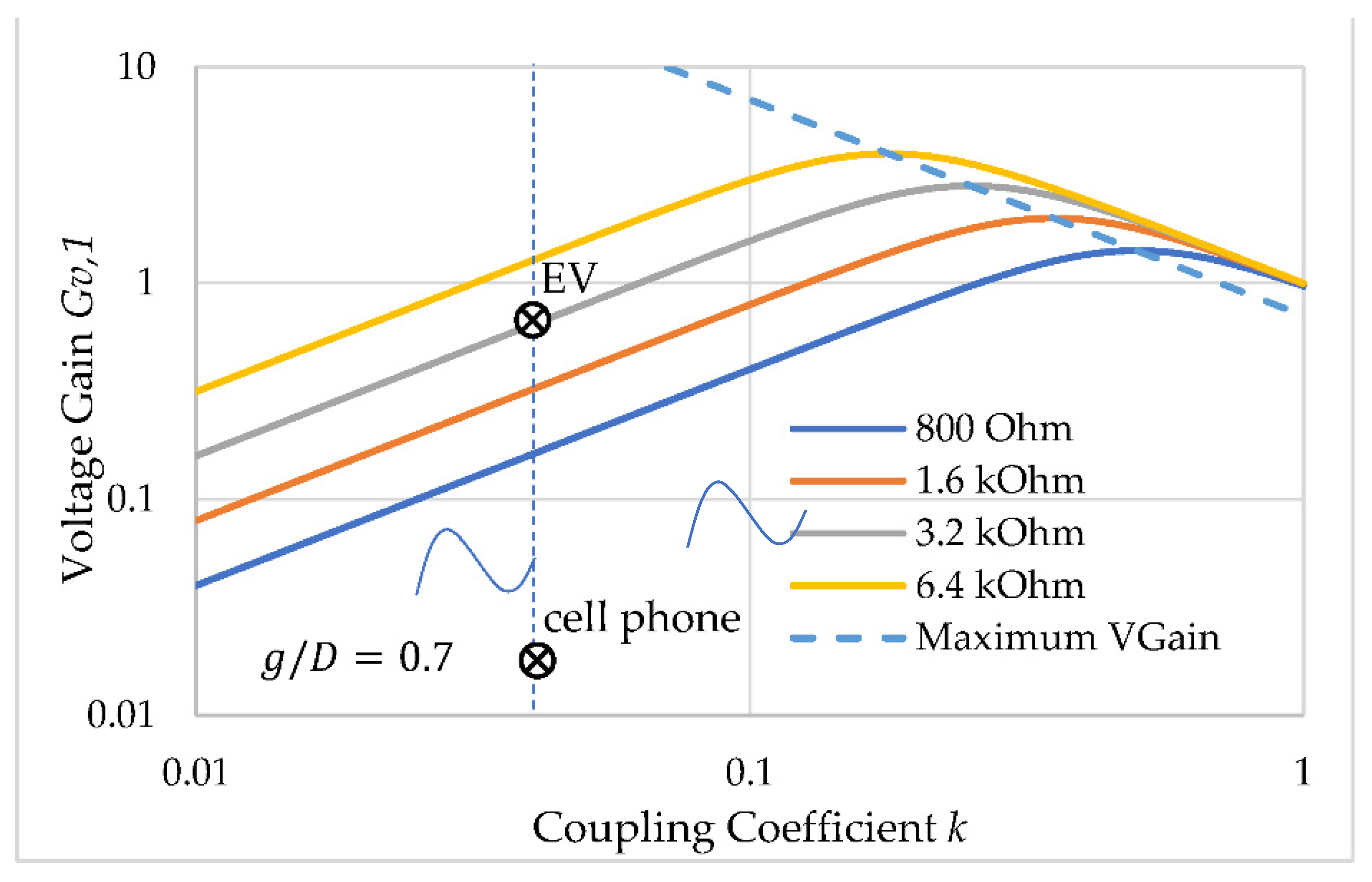
The coupling coefficient k is a function of distance gap g between the transmitting coil and the receiving coils used in the WPT. The factor of distance gap can be converted into the g / D ratio to simplify the actual effect to the coupling coefficient [9], where D denotes the coil diameter. The example which demonstrate the coupling coefficient decay with respect to different g / D ratio subjected to D = 70cm is shown in Figure 11. It can be seen the coupling coefficient k is 0.1 when the PRU coil is 35cm away from the PTU coil and the coupling coefficient k dropped into half of 0.1 when the PRU coil is 50cm away. It was also proposed in [9] that the maximum voltage gain G v , 1 as well as the maximum power transfer can be obtained when coupling coefficient k matches the parallel resonance quality factor Q P . It is then concluded that for the ultimately remote distance we have to use the zero resistance coils which might be easy to fulfill in the outer space but on the earth. The loading put in parallel with the LC tank can also affect the parallel resonance quality factor Q P as well, which causes the degradation of the voltage gain as shown in Figure 12. The battery voltage V B attached to the proposed PRU is a kind of loading which may be equivalent to the resistive loading when the charging current is flowing through the battery. For heavy load, i.e. smaller resistance equivalently, the voltage gain is smaller and thus a smaller equivalent resistance among the power transfer could be achieved when the battery is charged with large current. As for the same battery voltage V B the equivalent resistance becomes smaller when subjected to larger current. It also implies that it is preferable to charge a longer battery string with higher voltage in order to reduce the equivalent resistance. In an EV application, where the battery voltage can be as high as 300V could be an ideal application for the resonant WPT to transfer high power.
Different applications including the cell phone charging with voltage V B = 5 V under the charging current is 1A and the EV charging with V B = 132 V under the same charging current is 1A are used for comparison. Using C r = 200 pF and C P = 5nF , the voltage division is 25 times according to equation (15). For the case of cell phone battery charging the equivalent resistance is 5 Ω × 25 = 125 Ω , the voltage gain could be as small as 0.02 when g / D = 0.7 . For the case of EV battery charging the equivalent resistance is 132 Ω × 25 = 3.3 k Ω , the voltage gain could be as small as 0.8 for the same distance g / D = 0.7 . It has to be a higher V D D input in order to charge the cell phone than that of the EV application due to their equivalent loading differences as shown in Figure 12.

4. Simulation and Experiment

4.1. Simulation

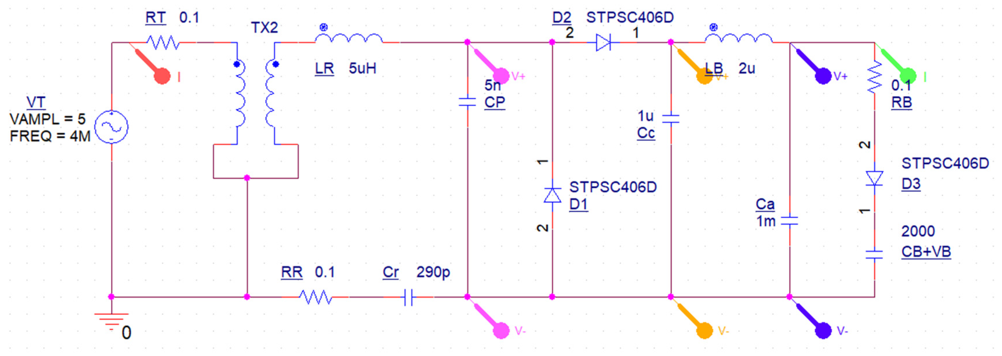
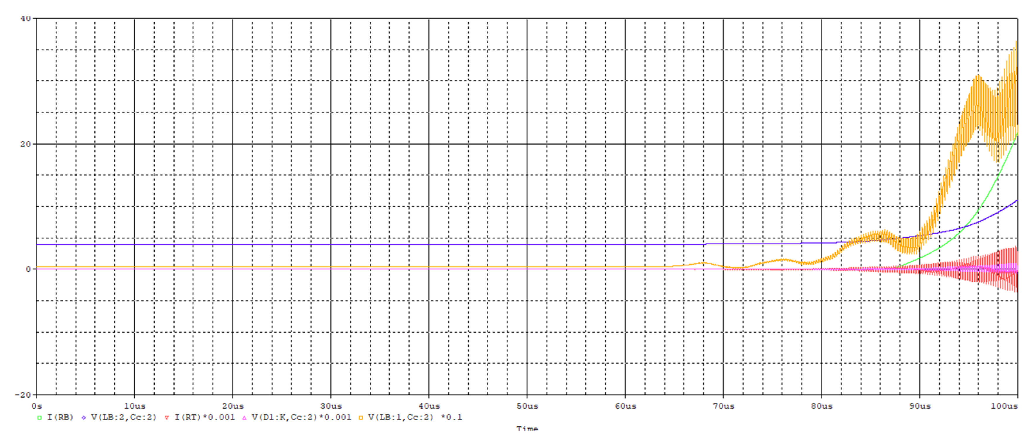
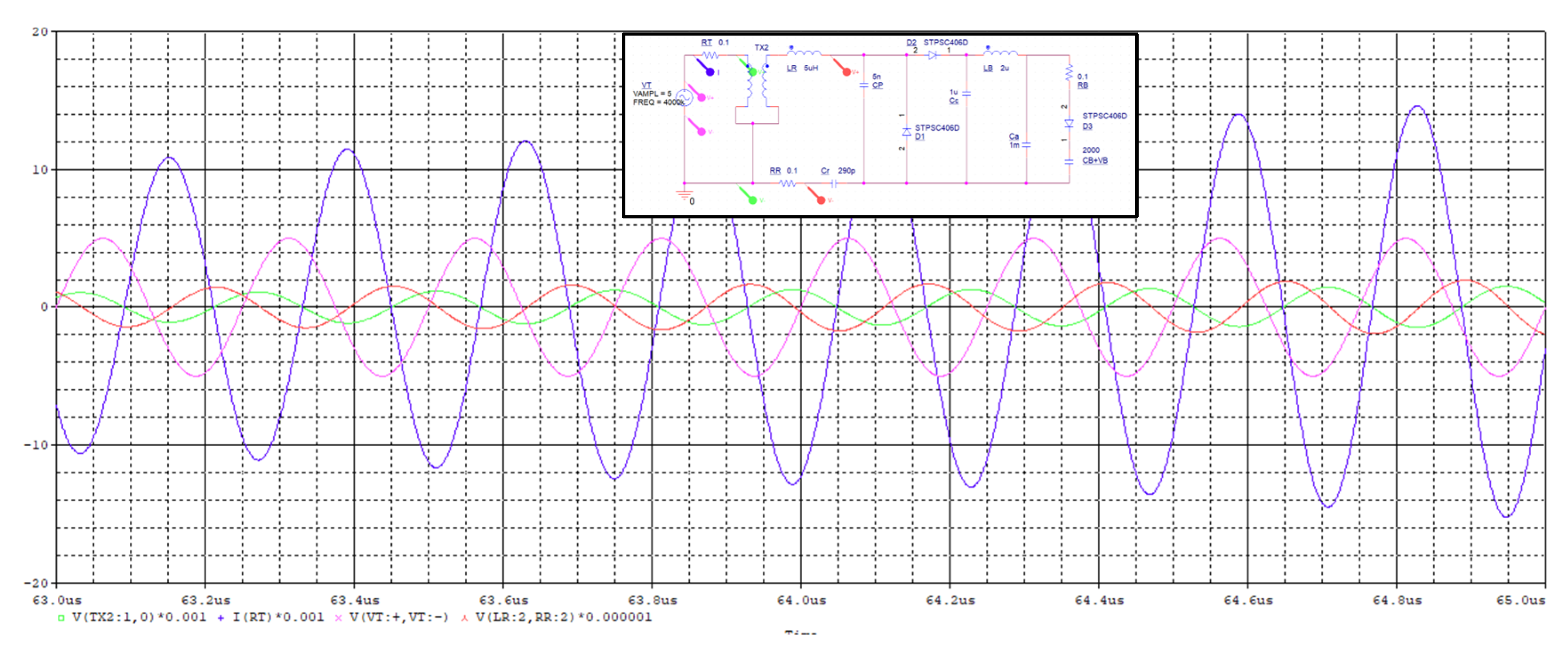
We adopted two simulations one is used to identify the effect of PRU alone and the other is to identify the PRU function inside of the resonant WPT with class E amplifier. The first simulation is shown in Figure 13, which applied the circuit parameters as shown in Table 2. Both the battery capacitor and the stabilization capacitor C a are initialized with the voltage 4V. The instability current can be observed in Figure 14 that the charging current toward he capacitor ramps up quickly after 100us simulation time. The circuit becomes unstable which goes to Mega-watt charging to the battery in 300us simulation time. It was due to the PRU AC-DC output capacitance C c (scale 10:1; in gold color line) is charged with high enough voltage to feed into the PRU stabilization capacitance C a (in blue color line). The battery charging current (in green line) dramatically rises when the voltage in C a reaches above the battery voltage plus the diode threshold voltage, which simultaneously brings up the input current (scale 1000:1; in red line). Both PRU resonant capacitor and the AC voltage divider capacitance voltages rises up due to the current resonance. Taking a closed examine on the phase change of the voltage and current with different color markers on the same circuit as shown in Figure 15, we zoom into the time duration between 63us to 65us before the power burst was happening. Compared to the time (phase) basis is on the input 5VAC (in purple line), the voltage v T (scale 1000:1; in green line) on the primary winding varies from a 20 0 phase lead at 63us to nearly 120 0 phase lead at 65us. The voltage v R (scale 10 6 :1; in red line) on the primary winding varies from a 220 0 phase lag at 63us to nearly 90 0 phase lag at 65us. It is also when the voltage v R and the voltage v T comes into a 90 0 phase, yielding a resonance condition satisfying equation (5) and (6) with the voltage gain | G v , 1 | nearly 1000 times.
Although this simulation is unreal in the wireless power transfer as the voltages cannot be as high as 1Mega-volt in real application when most of capacitor endures only thousands of volts, and also the voltage gain | G v , 1 | cannot be 1000 for long distance power transfer with low coupling coefficient k , it is still very valuable to understand the resonance mechanism as well as the proper function of the PRU circuit from this simulation example. It can be observed from Figure 14 that the voltage in the capacitor C c is oscillating in a subharmonic frequency around 10kHz. The current ramp is in a sense of exponential growth form which is known as the instability. The battery voltage V B is 4V in the simulation because it takes very long simulation time to reach the instability of the current when a larger battery voltage is applied. In the experiments we will use high battery voltage to attain the similar instability current effect.
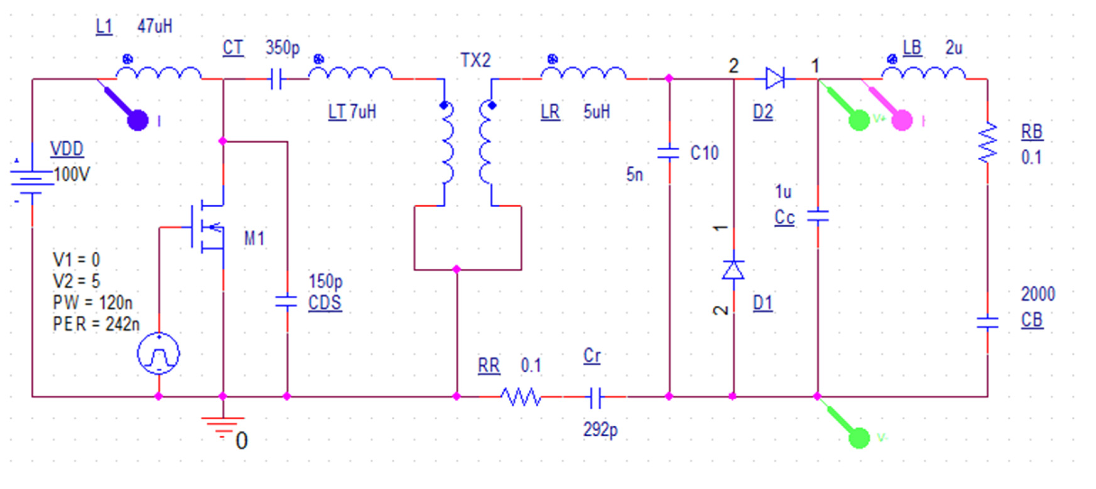
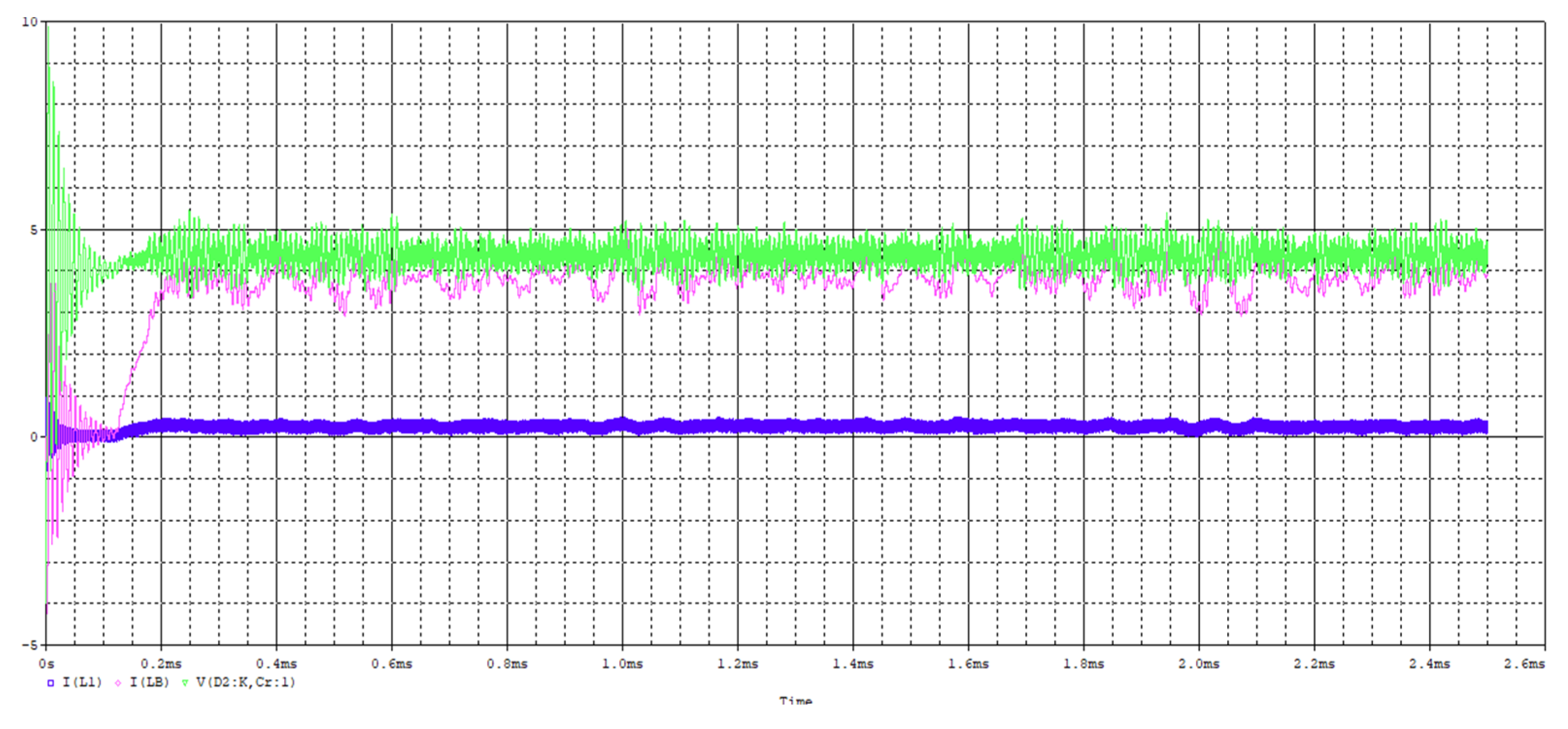
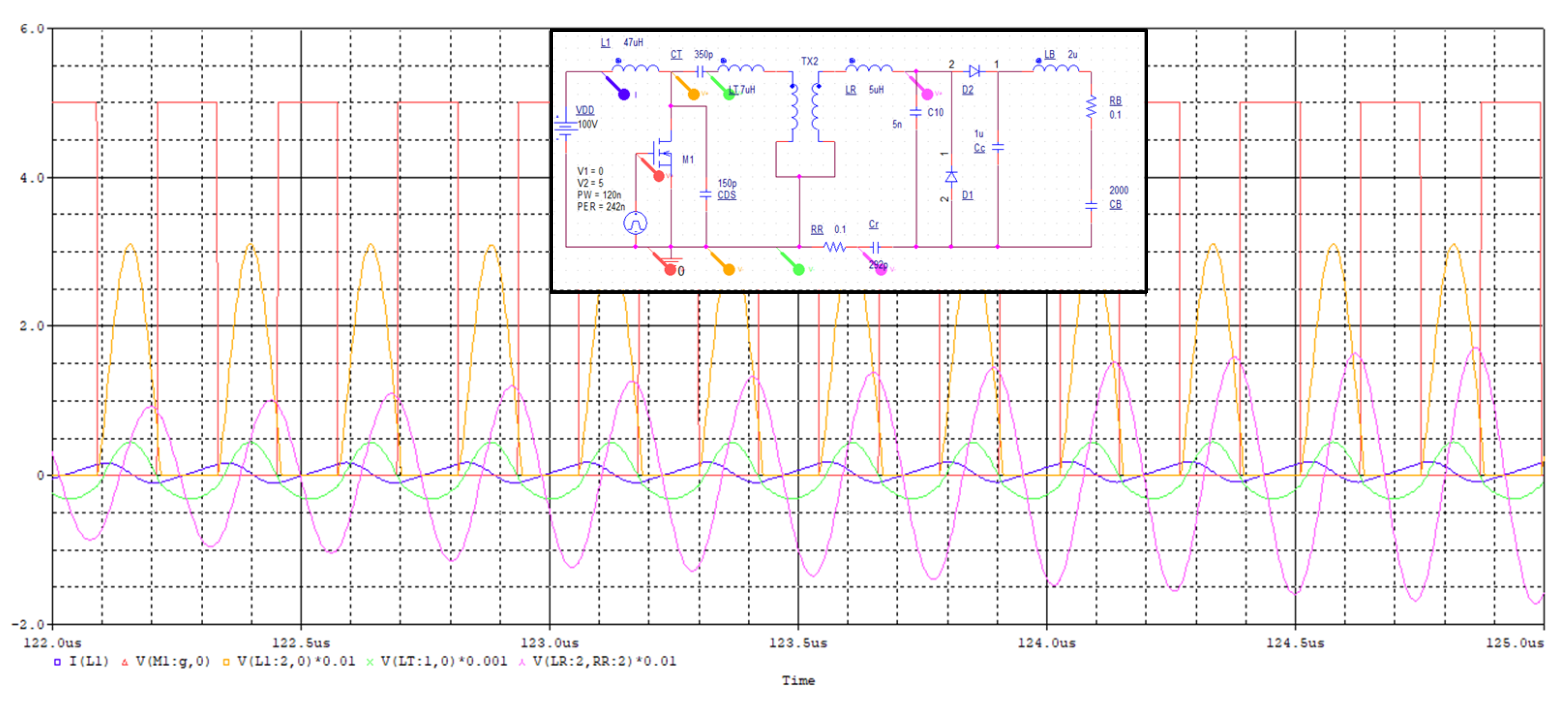
The second simulation is based on the class E amplifier instead of an AC voltage source, which can easily deliver high power with high voltage in high frequency around 4MHz. The class E amplifier was similar to the boost converter except the output is a LC tank as shown in Figure 16. In the circuit, all parameters used for PRU are identical to the previous simulation example except for the resonance capacitance C r is micro adjusted to 392pF for the resonance and also the stabilization capacitance is omitted from the circuit. The resonance occurs immediately after the circuit is turned on in the simulation, which does not need a stabilization capacitance to assist. The reason why the circuit can some into the resonance much faster than that of using the AC voltage source may be due to the precise matching of the resonant frequency or the class E amplifier is self-adjusting to the resonance. The corresponding results is shown in Figure 17. The AC-DC output capacitor C c first oscillates a while before reaching the voltage higher than the battery voltage, i.e. 4V and soon after the charging current rose up and reaches a 4A level. The charging current carries still some high frequency ripple same as indicated in the wide-band filter result of equation (20). The input current comes after the rising charging current. Since the battery voltage is set to 4V, the output power is calculated as 4A × 4V = 16W. There was no negative resistance effect of PRU occurred in previous example because of the steady state exists for the class E amplifier circuit. Taking a closer look in the time duration between 122us to 125 us before the charging current ramped up as shown in Figure 18, we observed that the ZVS is gradually forming from the wave form of transistor v D S (scale 100:1; in gold line) when it is compared to the v G S (in red line) turn-off time. It is also observed that the phase difference between the voltage v T (scale 1000: 1, in green line) of the primary winding and the voltage v R (scale 100: 1, in green line) of the secondary winding is becoming 90 0 which matches the resonance condition in equation (6). The current I 1   on inductor L 1 rises up during the transistor turn on time and the current phase angle ϕ is around 64 0 and the corresponding voltage magnification V x , m a x / V D D is also around 3.28 as expected in equation (2) of section 2.1 for the steady state. It shows that the class E amplifier can work just fine with the proposed PRU module. In this simulation, the switching frequency is 1000/242 = 4.1MHz and the duty is 120/242 = 49.6%. The voltage gain | G v , 1 | calculated from Figure 18 is 120V/500V = 0.24 which is achievable in the real resonant WPT application with quite a distance between PTU and PRU in the measure of diameter of the PYU coil.
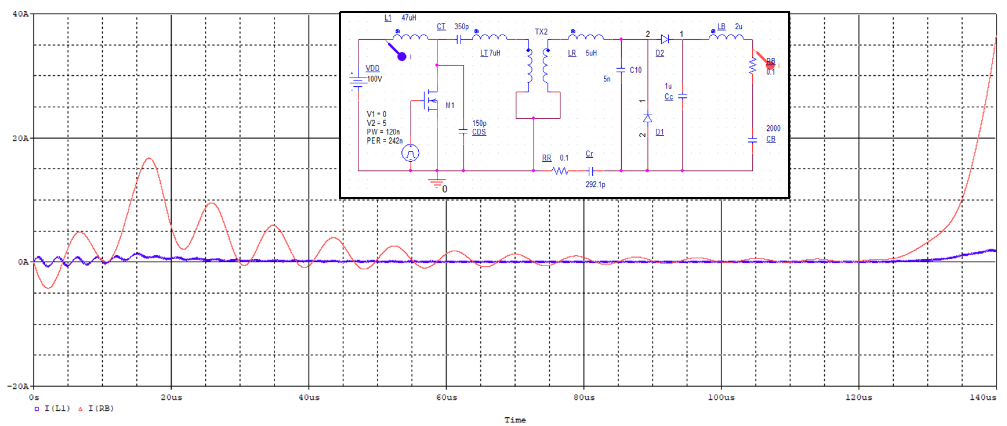
The control system will become unstable when the resonance with very high voltage gain | G v , 1 | can be achieved by adjusting the PRU resonance capacitance. Figure 19 shows the instability response when the resonance capacitance C r is micro adjusted to 292.1pF. With slight variation of the resonance capacitance C r , the LC tank changes from the stable circuit become an unstable circuit. An on-line monitoring of the PRU is therefore needed in practical application, the PTU may be controlled to avoid the instability. Both simulations above were using the same coupling coefficient k = 1 since the instability phenomenon will still happen with different coupling coefficients only the simulation time to reach instability will increase due to smaller value of coupling coefficient k . When we examine the output wave form (red curve trace) of the charging current flowing into the battery, we observe the subharmonics f s / n around 100kHz and other lower frequencies.

4.2. Experiment

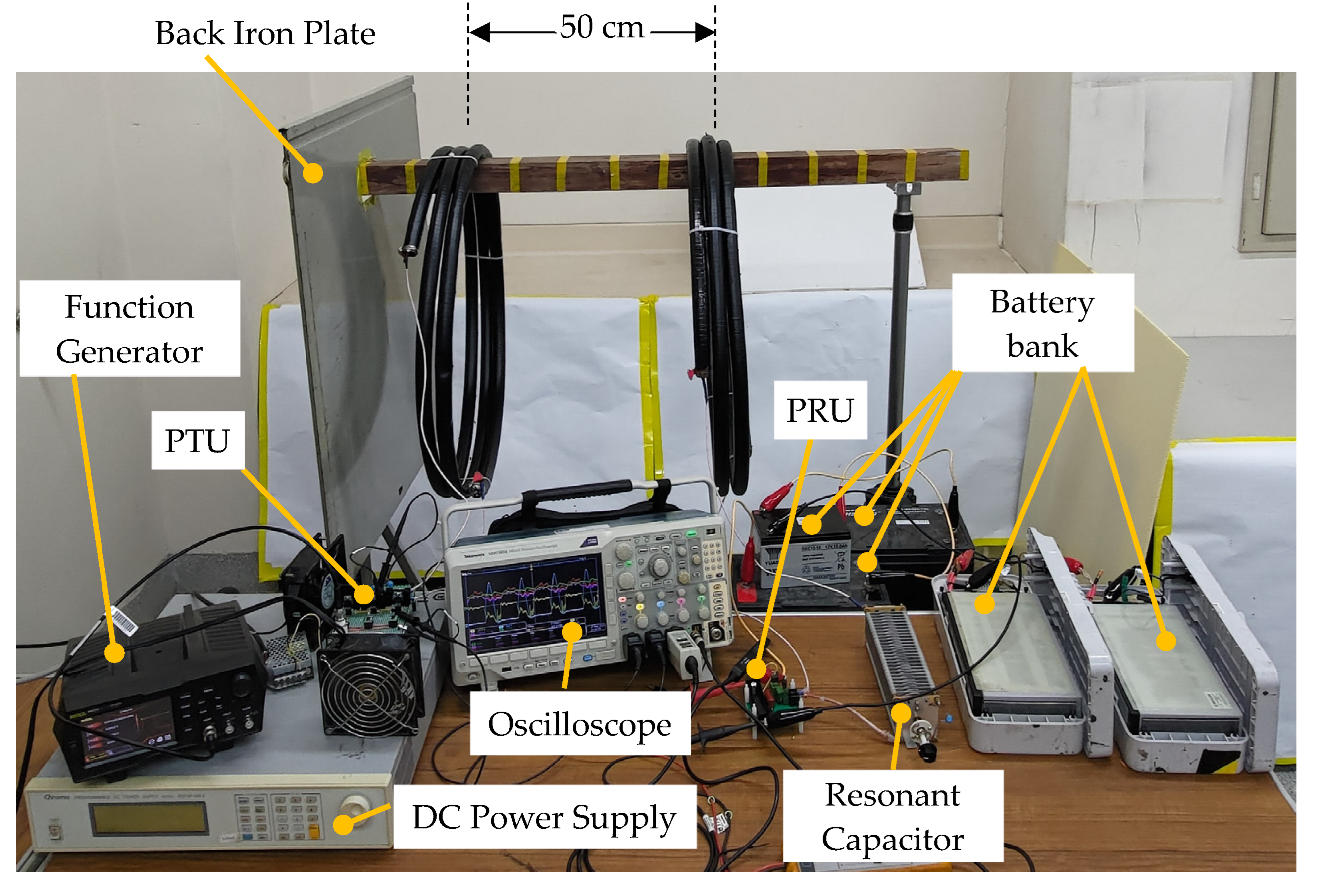
The experimental layout includes a PTU consisting of a class E amplifier and a transmitter coil, a PRU consisting of the PRU circuit and a receiving coil, a DC power supply, and a function generator to control the PTU switch as shown in Figure 20. The back-iron plate is isolated from all devices. The two coils are placed 50cm away from each other measured from the center of the coils. The PTU switch integrates three 20mm GaN devices connected in parallel which are all D-mode GaN HEMT driven by the charge pump gate drive. The resonant capacitor is in series of a ceramic capacitor with an adjustable capacitor which uses to tune the resonance capacitance to match with the switching frequency of the PTU switch. Each of the 20mm GaN device is able to conduct 6A DC current. In the class E amplifier, the maximum current flowing on the switch is 2.5 times as the DC current read from the power supply when the duty cycle of switching is 50%. Therefore, the maximum power allowed to deliver from the PTU under VDD = 90V input is 3 * 6 / 2.5 * 90 = 600W. Considering the switching loss among the GaN HEMT switches, we have to confine the experiment the maximum output power from the DC power supply within 350W by setting the maximum current output of the DC power supply into 3.5A. The battery string we used in the experiments, consists of two 48V Lithium battery packs and three 12V Lead-acid batteries which are all for different EV application. The batteries were connected in series, which together shows 132V as terminal voltage. The purpose of this experiment is demonstrating the EV battery charging with 1A current using the resonant WPT techniques with the PRU.
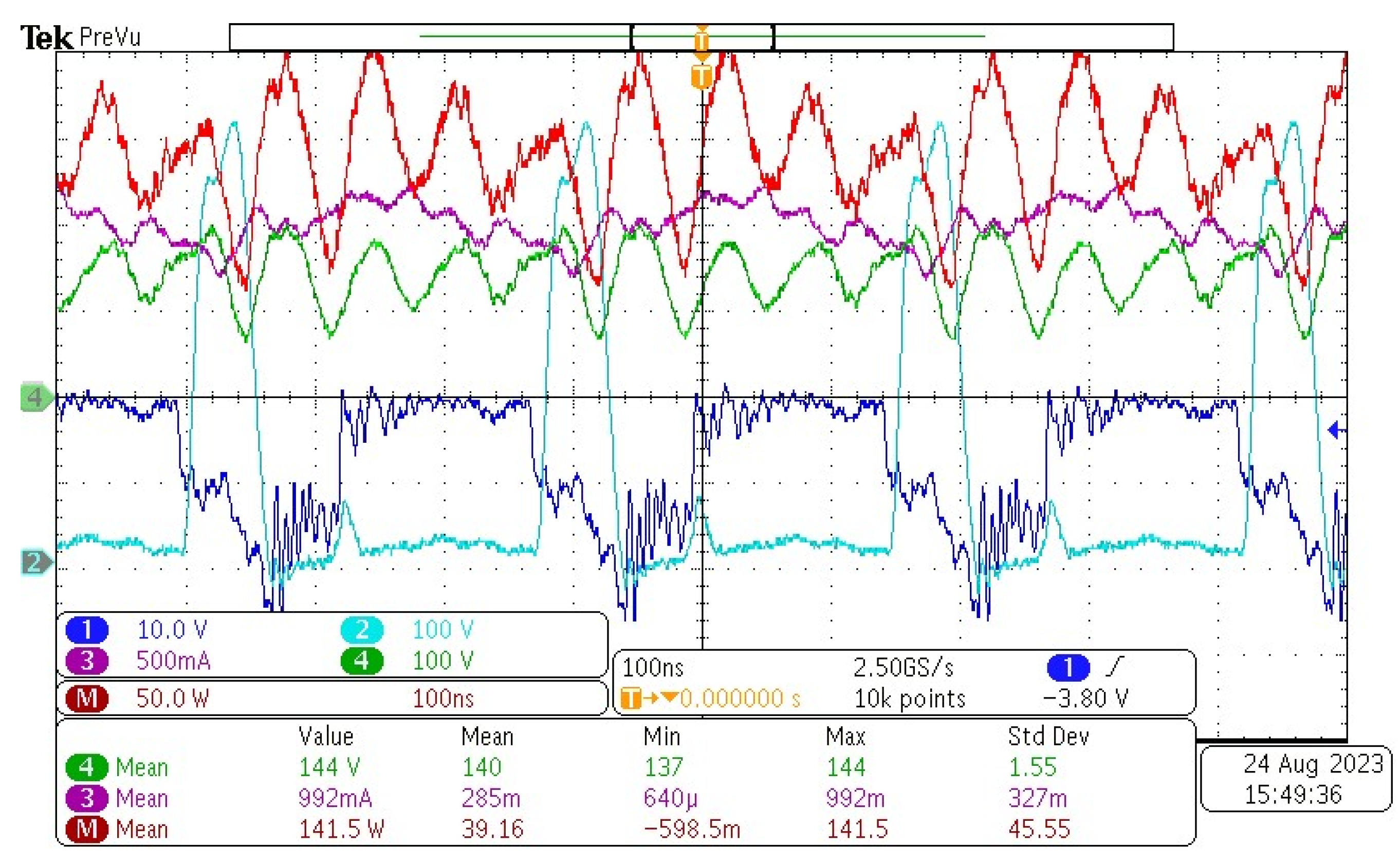
Figure 21 shows the oscilloscope screen dump at one instance during the battery charging. The dark blue color trace shows the V G S of one of the D-mode GaN HEMT switch which is with a threshold voltage of -7V for turning on the switch, which indicates also the duty of switching is 0.5, i.e. there is 50% of the time V G S is below -7V. The cyan color trace shows the V D S of one of the D-mode GaN HEMT switch which is with a maximum V D S as 500V, which is actually as high as 700V before the current limiting is reached. The green trace shows the battery voltage V B which is oscillating between 200V to 80V during the battery charging. The purple trace shows the battery current I B flowing through the battery string, which shows the average charging current of 992mA and no discharging current flowing through the battery even when the battery voltage is below 132V. From the positive charging current point of view, it may be concluded that the battery voltage oscillation may be due to the measurement of connection wire between the batteries via the high frequency magnetic flux. The red color trace shows the calculation done by the oscilloscope internally, which shows an average of 141.5W going into the battery charging.
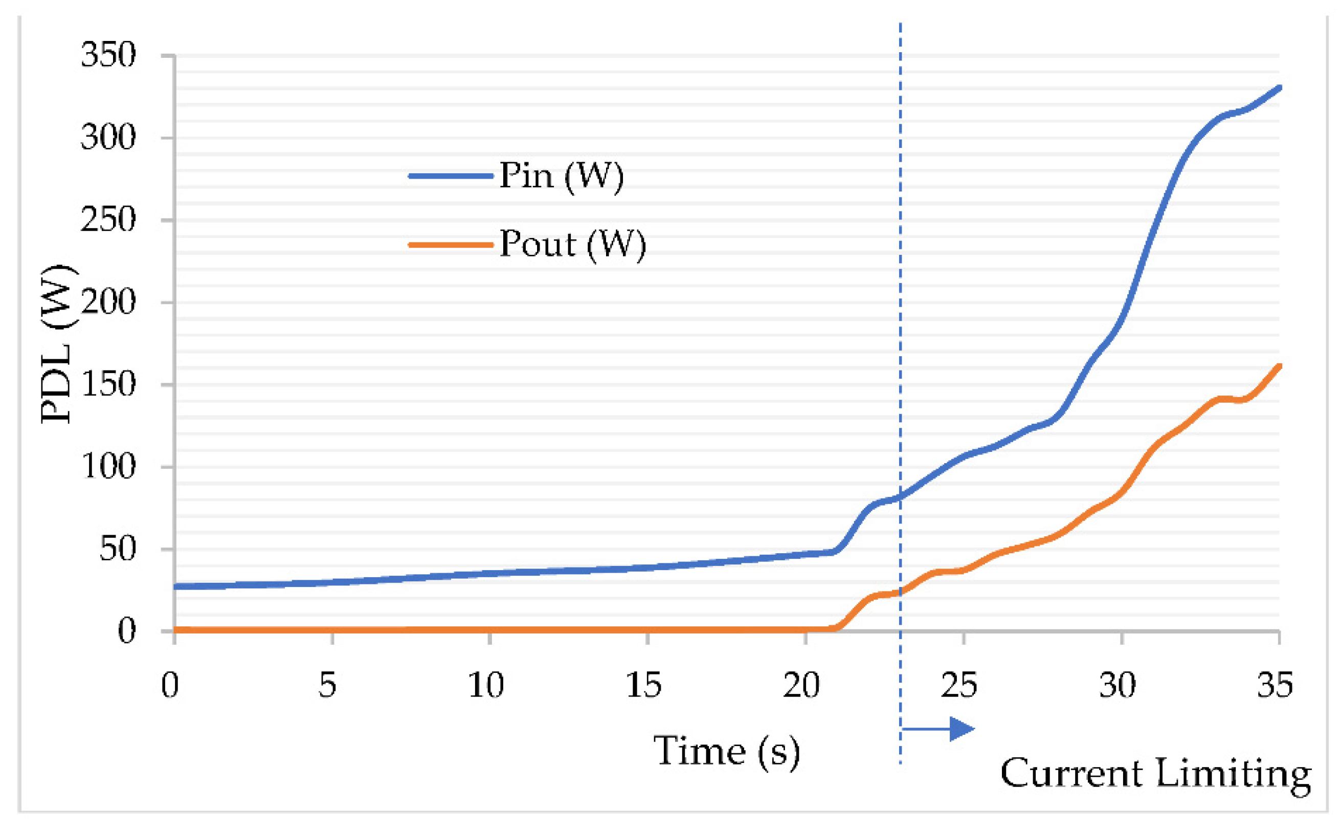
Figure 22 shows the power delivery to load (PDL) starting from the time we turn on the power supply until the time when the power supply reaches its current limit 3.5A. It took about 21 seconds for the PTU and PRU to form the perfect resonance. The PDL becomes unstable after 21 seconds, which ramps up until the current limit of the DC power supply is reached. The instability phenomenon agreed with both the simulation results as well as the theory of negative impedance converter via the sub-harmonic oscillation. The subharmonic oscillation had successfully converted the low frequency current back into the transmitting coil as a current feedback to the closed-loop of the resonant WPT. Although the detailed physics are still left behind to be explored, the experimental result matched the simulation results for instability current surge. The current limiting function is activated at the time of 34 seconds, after that the voltage of the DC power supply dropped and the power output will still be increasing for several seconds before it dropped down to 60% of the maximum PDL.
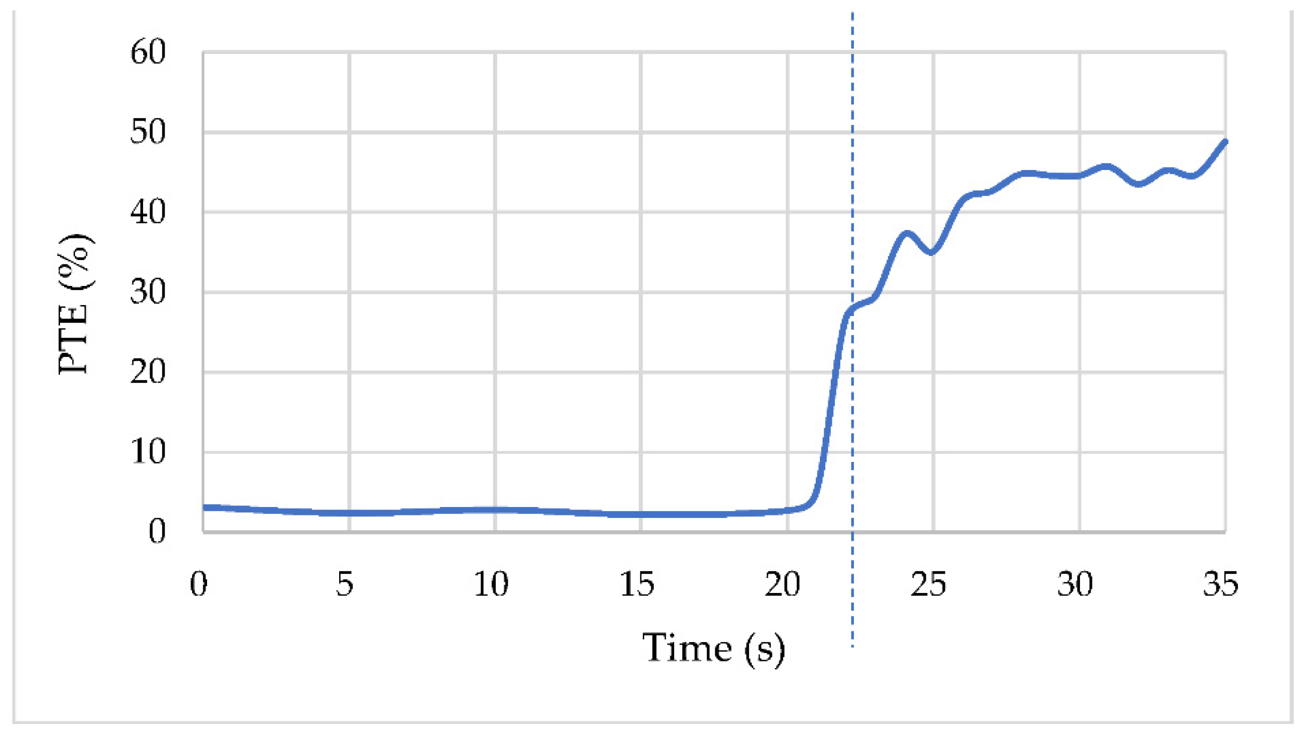
Figure 23 shows the power transfer efficiency (PTE) of the resonant WPT. The PTE grows simultaneously when the instability current shows, which is showing 50% of efficiency in this experiment. In other experiments, there is 65% PTE can be delivered with lower battery voltage which is with lower PDL that extends the time when the current limiting from the DC power supply. The PTE remained at 50% when the current limiting is reached. The PTE rises simultaneously with the PDL rising that is favorable to higher power transfer when more D-mode GaN HEMT transistors can be connected in parallel in the future.

5. Conclusions

This paper disclosed a specific circuit which is useful to be the power receiving unit (PRU) of the resonant WPT for acquiring high power from the power transmitting unit (PTU) automatically. The experiment is showing one ampere charging current is flowing into a 132V battery string with a 150W power transfer from 50cm away which is useful in the EV charging. The PTU consists of a voltage divider using the capacitors, an AC-DC converter using a pair of high voltage FRD diodes and a flat-band band-pass filter for the 4MHz resonant WPT. The capacitive voltage divider has its merit on separating the output loading from the LC tank for resonance. The PRU performed as a negative impedance converter uses only the diodes and the capacitors, which uses all passive elements and needs no power source from the equipment that is attached to the PRU. When the PTU switching frequency matches the PRU resonance frequency, the phases of the PTU output current as well as transmitting coil voltage and receiving coil voltage will be self-organizing to deliver a high power in a negative damping resonance which induces an instability current ramp and produces high power transfer. This instability current phenomenon is a nonlinear effect due to different harmonics of the current can yield different impedance features. With the flat-band feature, the PRU is able to present itself as a negative resistance behavior on the middle frequency band and an inductor behavior in the high frequency band. The nonlinear behavior in this paper interpreted as the subharmonic oscillation whose nonlinearity could be due to the nonlinearity of the rectification diodes used in the PRU. When the high frequency AC source is implemented using the GaN HEMT transistor and class E circuit, the nonlinear behavior still persisted. It will depend on the constant current control of the specific DC power supply is used when the current limiting of the DC power supply is reached. In our experiment, the voltage from the DC power dropped to a voltage without causing the PTE degeneration however the PDL dropped. The resonant WPT proposed in this paper with the PRU in its negative impedance converter nature is still an open-loop system, which may be improved with a closed-loop control when the instability is fully comprehended. We will continue to do research on the subharmonic oscillation theories to explore the possible control to regulate the PTU output current for sustaining the WPT in its high PDL when the PRU in this type is used. Furthermore, we are fabricating many more 20mm D-mode GaN HEMT devices and integrating them together into a higher current switch for the PTU in the future.

Funding

This research was funded by National Science and Technology Council, R.O.C., grant number NSTC 112-2622-8-a49-013-sb. In part, this work was also financially supported by the “Center for the Semiconductor Technology Research” from The Featured Areas Research Center Program within the framework of the Higher Education Sprout Project by the Ministry of Education (MOE) in Taiwan.

Institutional Review Board Statement

Not applicable.

Informed Consent Statement

Not applicable.

Data Availability Statement

Data sharing not applicable.

Acknowledgments

The authors also thank You-Chen Weng of the CSD Lab for fabricating the D-Mode MIS-HEMT chips and IMLab graduate students for their help in the experimental setup.

Conflicts of Interest

The authors declare no conflict of interest.

References

  1. Zhang, Z., Pang, H., Georgiadis, A., Cecati, C. Wireless power transfer—An overview. IEEE transactions on industrial electronics, 66(2), 2018, pp. 1044–1058. [CrossRef]
  2. Mahesh, A., Chokkalingam, B., Mihet-Popa, L. Inductive wireless power transfer charging for electric vehicles–a review. IEEE Access, 9, 2021, 137667-137713. [CrossRef]
  3. Green, P. B. Class-E power amplifier design for wireless power transfer. August 2018. Rev 1.2. Infineon, Appl. Note 1803, pp. 1–51. Available online: infineon.com (accessed on August 2018).
  4. Paolucci, M.; Green, P. B. Benefits of GaN e-mode HEMTs in wireless power transfer - GaN power devices in resonant class D and class E radio frequency power amplifiers. October 2018. Rev 1.0. Infineon, White Paper. Available online: infineon.com (accessed on October 2018).
  5. Choi, J., Tsukiyama, D., Tsuruda, Y., Davila, J. M. R. High-frequency, high-power resonant inverter with eGaN FET for wireless power transfer. IEEE Transactions on Power Electronics, 33(3), 2017, pp. 1890–1896. [CrossRef]
  6. Sinha, S., Regensburger, B., Kumar, A., Afridi, K. A very-high-power-transfer-density GaN-based capacitive wireless power transfer system. In 2017 IEEE 5th workshop on wide bandgap power devices and applications (WiPDA), 2017, pp. 360-365.
  7. Abou Houran, M.; Yang, X.; Chen, W. Free Angular-Positioning Wireless Power Transfer Using a Spherical Joint. Energies 2018, 11, 3488. [CrossRef]
  8. F. Jolani, Y. -q. Yu and Z. Chen, "A planar positioning-free magnetically-coupled resonant wireless power transfer," 2015 IEEE Wireless Power Transfer Conference (WPTC), Boulder, CO, USA, 2015, pp. 1-3. [CrossRef]
  9. Liu, C.-Y.; Wu, C.-C.; Tang, L.-C.; Shieh, Y.-T.; Chieng, W.-H.; Chang, E.-Y. Resonant Mechanism for a Long-Distance Wireless Power Transfer Using Class E PA and GaN HEMT. Energies 2023, 16, 3657. [CrossRef]
  10. Larky, A. Negative-impedance converters. IRE Transactions on Circuit Theory, 4(3), 1957, pp.124–131.
  11. Yoon, S. H., Kim, T. H., Yook, J. G., Yun, G. H., Lee, W. Y. High Q-factor WPT system with negative impedance converter. In 2017 IEEE Wireless Power Transfer Conference (WPTC), 2017, pp. 1–4).
  12. Kim, T. H., Yun, G. H., Lee, W., Yook, J. G. Highly efficient WPT system with negative impedance converter for Q-factor improvement. IEEE Access, 7, 2019, 108750–108760. [CrossRef]
  13. Liu, Y.; Li, B.; Huang, M.; Chen, Z.; Zhang, X. An Overview of Regulation Topologies in Resonant Wireless Power Transfer Systems for Consumer Electronics or Bio-Implants. Energies 2018, 11, 1737. [CrossRef]
  14. E. Abramov, Y. Schultz, M. Evzelman, and M. M. Peretz, “Analysis and design of post-regulation stages for resonant capacitively-coupled wireless power systems,” in Proc. IEEE Appl. Power Electron. Conf. Expo., 2022, pp. 492–499.
  15. Harmonic and Subharmonic Oscillations. Available online: https://phys.libretexts.org/Bookshelves/Classical_Mechanics/Essential_Graduate_Physics_-_Classical_Mechanics_(Likharev)/05%3A_Oscillations/5.08%3A_Harmonic_and_Subharmonic_Oscillations.
  16. Weng, Y.-C.; Wu, C.-C.; Chang, E.Y.; Chieng, W.-H. Minimum Power Input Control for Class-E Amplifier Using Depletion-Mode Gallium Nitride High Electron Mobility Transistor. Energies 2021, 14, 2302. [CrossRef]
  17. Liu, C.-Y.; Wang, G.-B.; Wu, C.-C.; Chang, E.Y.; Cheng, S.; Chieng, W.-H. Derivation of the Resonance Mechanism for Wireless Power Transfer Using Class-E Amplifier. Energies 2021, 14, 632. [CrossRef]
  18. Hayashi, C. Subharmonic oscillations in nonlinear systems. Journal of Applied Physics, 24(5), 1953, pp. 521–529.
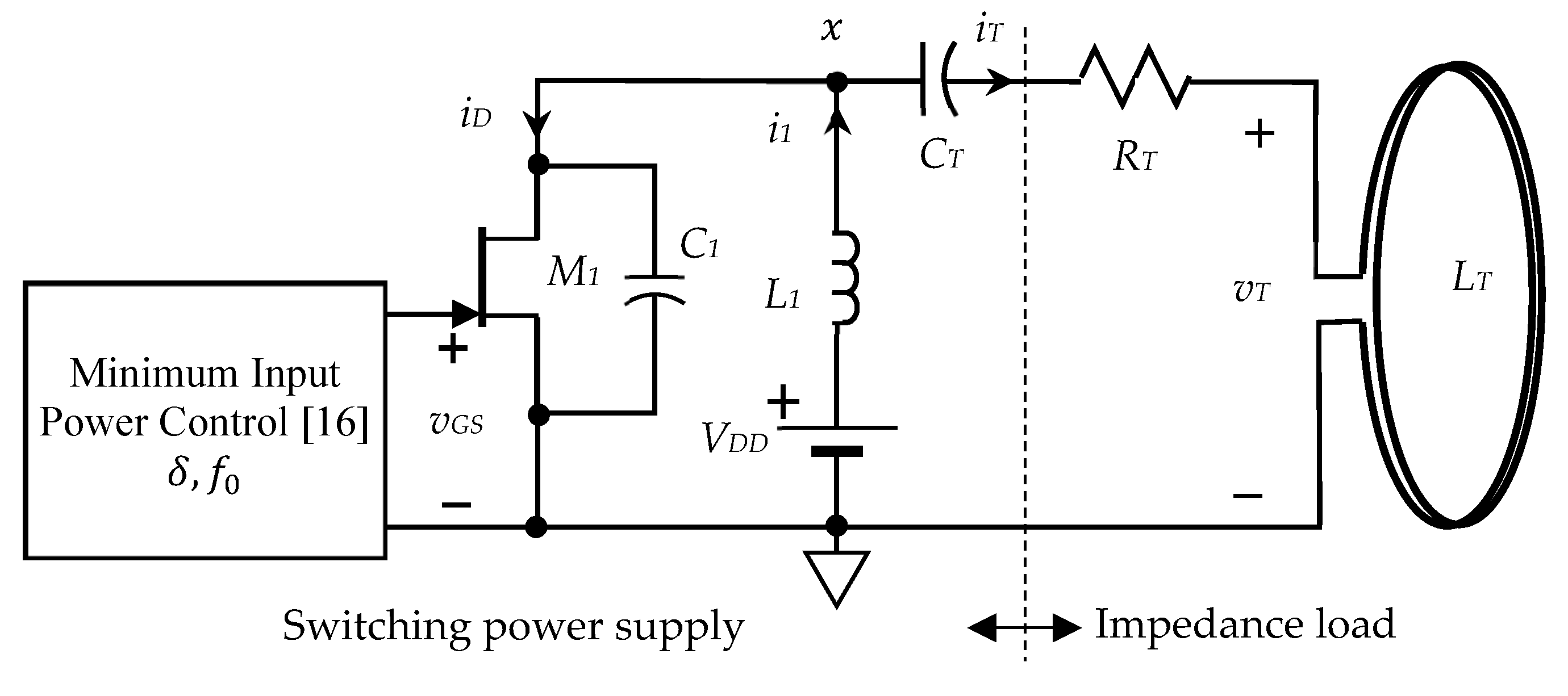
Figure 1. Power transmitting unit (PTU) using class E amplifier.
Preprints 88474 g001
Figure 2. The current wave form of PTU and the current phase angle ϕ .
Preprints 88474 g002
Figure 3. The proposed power receiving unit (PRU).
Preprints 88474 g003
Figure 4. Transformer circuit model for WPT.
Preprints 88474 g004
Figure 5. Power transmitting unit (PTU) using class E amplifier.
Preprints 88474 g005
Figure 6. The AC-DC Converter circuit.
Preprints 88474 g006
Figure 7. The capacitive voltage divider circuit.
Preprints 88474 g007
Figure 8. The flat-band band-pass filter circuit (a) without stabilization capacitor and (b) with stabilization capacitor C a .
Preprints 88474 g008
Figure 9. The admittance transfer function of flat-band band-pass filter.
Preprints 88474 g009
Figure 10. The equivalent circuit of resonant WPT for battery charging.
Preprints 88474 g010
Figure 11. Coupling coefficient vs. distance of power transfer.
Preprints 88474 g011
Figure 12. The voltage gain in terms of coupling coefficient for different load resistance Zo when CT = 200 pF and L2 = 7uH.
Preprints 88474 g012
Figure 13. Simulation circuit for understanding the PRU functions.
Preprints 88474 g013
Figure 14. Resonance results with a PRU in the WPT application.
Preprints 88474 g014
Figure 15. Phase changes during the resonance formation.
Preprints 88474 g015
Figure 16. Simulation circuit for resonant WPT using class E amplifier.
Preprints 88474 g016
Figure 17. Simulation result for resonant WPT using class E amplifier with stable currents, the input current of the PTU (blue color) and the output current to the battery (purple color).
Preprints 88474 g017
Figure 18. Class E amplifier responses for resonant WPT, which shows the formation process of the resonance.
Preprints 88474 g018
Figure 19. The instability current with class E amplifier used in PTU including the input current of the PTU (blue color) and the output current to the battery (red color).
Preprints 88474 g019
Figure 20. The experiment layout.
Preprints 88474 g020
Figure 21. The wave forms of voltages and current from the oscilloscope including PTU V G S (dark blue color), PTU V D S (cyan color), PRU I B (purple color), PRU V B (green color), calculated power transfer (red color).
Preprints 88474 g021
Figure 22. The historical trend of input and output power from one experiment.
Preprints 88474 g022
Figure 23. The historical trend of power transfer efficiency (PTE) calculation from one experiment.
Preprints 88474 g023
Table 1. The 20 mm D-mode GaN HEMT parameters.
Symbol Description Unit VDS
0V 600V
Coss Output capacitance pF 31 17
Ciss Input capacitance pF 46 31
Crss Feedback capacitance pF 23 8
Vth Gate turn on voltage V −9
VGS Maximum V 10 ~ −30
RDS,on On resistance m Ω 900
VBD Breakdown voltage V 600
iD,cont. Continuous drain current A 3
Table 2. List of Parameters in Simulation 1.
Item Description Unit Value
R T PTU coil resistance Ohm 0.1
R R PRU coil resistance Ohm 0.1
R B Battery resistance Ohm 0.1
L R Leakage inductance of WPT transformer uH 5
L M Magnetization inductance of WPT transformer uH 0.1
L B Band pass filter inductance uH 2
D 1 , 2 , 3 High voltage, fast recovery diode; SiC STPSC406D
C r PRU resonance capacitance pF 290
C P PRU AC voltage divider capacitance nF 5
C B Battery capacitance F 2000
C c PRU AC-DC output capacitance uF 1
C a PRU stabilization capacitance mF 1
k Magnetic Coupling Coefficient 1
V B Battery voltage V 4
Disclaimer/Publisher’s Note: The statements, opinions and data contained in all publications are solely those of the individual author(s) and contributor(s) and not of MDPI and/or the editor(s). MDPI and/or the editor(s) disclaim responsibility for any injury to people or property resulting from any ideas, methods, instructions or products referred to in the content.
Copyright: This open access article is published under a Creative Commons CC BY 4.0 license, which permit the free download, distribution, and reuse, provided that the author and preprint are cited in any reuse.
Prerpints.org logo

Preprints.org is a free preprint server supported by MDPI in Basel, Switzerland.

Subscribe

© 2024 MDPI (Basel, Switzerland) unless otherwise stated