Preprint
Communication

Ultra-Energy-Efficient Reversible Quantum-Dot Cellular Automata 8:1 Multiplexer Circuit

Altmetrics

Downloads

96

Views

50

Comments

0

A peer-reviewed article of this preprint also exists.

Submitted:

23 October 2023

Posted:

24 October 2023

You are already at the latest version

Alerts
Abstract
Energy efficiency considerations in terms of reduced power dissipation is a significant issue in the design of digital circuits for very large-scale integration (VLSI) systems. Quantum-dot cellular automata (QCA) is an emerging ultra-low power dissipation approach, distinct from the traditional complementary metal-oxide semiconductor (CMOS) technology, for building digital computing circuits. Developing fully reversible QCA circuits has the potential to significantly reduce energy dissipation. The multiplexer is a fundamental element in the construction of useful digital circuits. In this paper, a novel, multilayer, fully reversible QCA 8:1 multiplexer circuit, with ultralow energy dissipation, is introduced. The proposed multiplexer power dissipation is simulated using the QCADesigner-E version 2.2 tool, describing the microscopic physical mechanisms underlying the QCA operation. The results showed that the proposed reversible QCA 8:1 multiplexer consumes 89% less energy than the most energy-efficient 8:1 multiplexer circuit presented previously in the scientific literature.
Keywords: 
Subject: Engineering  -   Electrical and Electronic Engineering

1. Introduction

The advancement of complementary metal-oxide semiconductor (CMOS) technology has led to growing concern about its associated negative aspects, including subthreshold voltage and gate leakage current [1]. Additionally, the escalating demand for increasing the number of devices on the CMOS system on a chip, already at a count of billions, exacerbates the issue of excessive power dissipation [2]. Quantum-dot Cellular Automata (QCA) is a nascent computing concept, that employs cells containing four quantum dots, to perform computations at the nanoscale level. The QCA idea is based on a transistor less paradigm, where binary information is encoded, via the electron charge location, in four quantum dots of the QCA cell, at antipodal configurations [3]. QCA offers several advantages over conventional semiconductor-based technologies such as CMOS, including highly reduced power consumption, the potential for high-speed operation, and the ability to create high QCA cell density ‘nanochip’ integrated circuits. Designing QCA digital circuits using a reversible design technique can yield enhanced ultralow-energy dissipation circuits [4]. Theoretically, reversible computation operations, that maintain the reversibility from the synthesis to the physical layout of the circuit, can mitigate information loss and require zero accompanying energy dissipation [5]. In very large-scale integration (VLSI) systems, the multiplexer is a digital circuit that selects one of the input data lines, and forwards that selected data, to a single output line, based on a set of control signals. Multiplexers are pervasive in digital electronics and are used for data routing and selection purposes. In this work, a novel design for a multilayer reversible QCA 8:1 multiplexer circuit, that exhibits ultralow energy dissipation, is proposed. The novel multiplexer has reversibility in both the synthesis and layout of the circuit design. The QCADesigner-E version 2.2 software tool [6], which contains a microscopic quantum mechanical description of the cell behaviour, with a Hartree treatment of cell–cell electrostatic interaction, is employed to simulate the performance and energy dissipation of the design. The remainder of this paper is organized as follows: In Section 2, the fully reversible design concept is explained, for the novel multiplexer circuit. In Section 3, the hierarchical design process for the proposed fully reversible QCA 8:1 multiplexer circuit is presented. The simulation results are given and discussed in Section 4, and the conclusions of the current study are provided in Section 5.

2. Fully Reversible Design Concept

Conventional computing techniques commonly involve irreversible operations, resulting in the deletion of some of the input bits of data, during the computational process. This information loss is accompanied by the dissipation of energy, kBTln2 per bit erased, where kB is the Boltzmann constant and T is the temperature [7], a consequence of the second law of thermodynamics. Using reversible logic operations instead of the typical irreversible computations, maintains a one-to-one correspondence between input and output signals. Thus, from the outset, unlike irreversible computations, reversible operations have no information loss with the attending dissipation of energy into the environment. However, substantially reducing energy usage in reversible computing requires preserving reversibility down to the circuit physical level [4]. As a result, in the design synthesis, as well as at the architecture layout stage, the physical implementation of the circuit, must be reversible to avoid energy dissipation.
In recent years, scholars have grown increasingly interested in investigating the development of reversible QCA circuits [8,9,10,11]. Nevertheless, their designs highlight the reversibility of the circuit at the synthesis level, neglecting the potential loss of information arising from irreversibility, at the physical layout level. In 2020, a novel reversible design technique was proposed for the synthesis and layout of a combinational QCA half-adder circuit [12]. This innovative approach emphasizes preserving reversibility during the entire circuit design process, at all levels. The findings of this simulation and modelling research indicate that combinational QCA designs, which maintain reversibility down to the layout level, generate QCA circuits that dissipate less energy than the Landauer theoretical limit of kBTln2. However, they neglected the need for data synchronisation, which can affect the precision of the QCA digital circuit’s computation. The current authors have tackled this important time-synchronisation issue, by employing a circuit architecture that is intrinsically more symmetrical [13]. The novel fully reversible time-synchronised design technique was subsequently used to investigate, via simulation, more complex combinational QCA logic circuit designs [13,14], as well as sequential QCA circuits, that have internal feedback loops, by their nature [15].
In this paper, a novel fully reversible QCA 8:1 multiplexer circuit employing the fully reversible time-synchronised QCA design approach, with ultralow energy consumption, is designed and simulated. The primary cause of energy dissipation in QCA circuits is attributed to the use of conventional irreversible majority gates [16]. The proposed novel design uses a fully reversible majority gate, as its fundamental component. The VLSI hierarchical design process for designing a fully reversible 8:1 multiplexer in QCA, may be broken down into the stages:
  • Reversibly designing a QCA majority gate.
  • Reversibly designing a QCA 2:1 multiplexer containing three reversible majority gates and an inverter.
  • Reversibly designing a QCA 4:1 multiplexer containing three reversible QCA 2:1 multiplexers.
  • Reversibly designing a QCA 8:1 multiplexer containing two reversible QCA 4:1 multiplexers and an additional single reversible QCA 2:1 multiplexer.
The synchronization of data flow in logic circuits is crucial for ensuring accurate data transmission and functioning. For QCA circuits, an external clock is applied, to change the strength of the tunnelling barrier between the QCA cells, allowing the control of the timing. Numerous timing and clocking schemes have been suggested, to govern the transfer of information in QCA circuits [17,18,19]. Data flow synchronization in our proposed circuit is achieved by utilizing the unified, standard, and efficient (USE) timing approach [19]. The USE timing approach possesses a high degree of flexibility, allowing it to effectively meet the requirements of QCA circuit design. These requirements include the incorporation of feedback channels with varying loop sizes, the establishment of standardized cell libraries, and the promotion of simplified routing. The USE clocking system consists of four time zones labelled from 1 to 4. Each time zone, which consists of a cluster of five-by-five QCA cells, represents a distinct time period. The combination of these four time zones, constitutes a complete clock cycle. The reader is referred to the papers [11,12,13,14] for further details.
One of the most challenging issues encountered when designing digital logic circuits, pertains to the handling of wire junctions. In this study, the wire crossing problem is solved by using the multilayer technique developed by Bajec and Pecar [20]. This technique is used to design a reversible QCA 8:1 multiplexer circuit, with three distinct layers, to solve the wire junction issue.

3. Design Process of the Proposed Fully Reversible QCA 8:1 Multiplexer

The primary goal of this study is to create a QCA 8:1 multiplexer circuit, that has exceptionally low energy consumption. Hence, a fully reversible design methodology that inherently overcomes the information loss issue, has been utilized. The design process involved several stages of development and represents an application of hierarchical design.

3.1. Reversible Majority Gate

The majority gate is the fundamental logic gate, used in QCA, that determines the majority value for its three inputs, i.e., a majority voting behaviour. It is mathematically represented in Equation 1.
M A ,   B , C = A B + A C + B C ,
The majority gate is widely recognized as the principal contributing factor to energy dissipation in QCA circuits [16]. The conventional majority gate in QCA exhibits irreversibility due to the salient point is that it has three input pins and only a single output pin. As a result, of the information loss consisting of two output pins, the second law of thermodynamics demands that there is heat dissipation, into the environment.
Consequently, our initial focus was in developing a fully reversible majority gate with three inputs and three outputs. The fully reversible majority gate replicates the data for two inputs, labelled A and B into two outputs labelled A Copy and B Copy, resulting in an overall situation, with equal numbers of binary inputs and outputs respectively (see Figure 1). Figure 1a illustrates a schematic depiction of the logical design, while Figure 1b shows the cell layout design of the fully reversible QCA majority gate. In this research, the fully reversible majority gate is the main building ‘block’ in the development of the fully reversible QCA multiplexer.

3.2. Reversible 2:1 Multiplexer

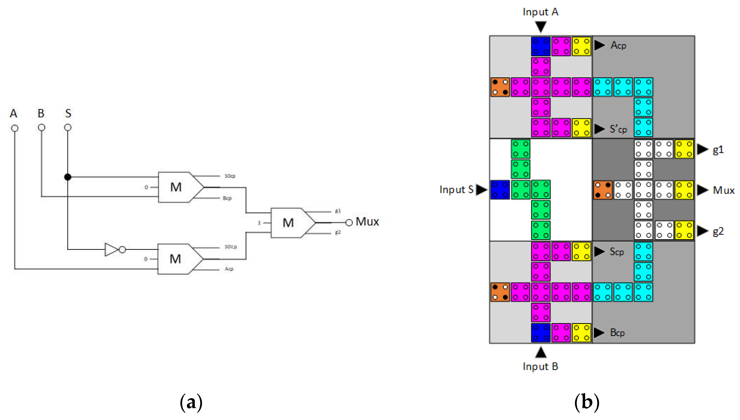
The next step of the design process, for the fully reversible QCA 8:1 multiplexer circuit, is the creation of a fully reversible QCA 2:1 multiplexer circuit, which serves as the central ‘organ’ of the design. The 2:1 multiplexer considered in this study, utilizes the fully reversible majority gate, presented in Section 3.1, as a main building element. The reversible 2:1 multiplexer is composed of three fully reversible majority gates and one inverter, as shown in Figure 2. The circuit synthesis diagram is depicted in Figure 2a, and its QCA cell layout design is shown in Figure 2b. The delay of the reversible QCA 2:1 multiplexer is four clock zones, which is equal to one complete clock cycle. This design requires the use of 56 QCA cells, occupying a total area of 0.09 µm2, for the underlying technology geometric parameters given in Table 1.
The Boolean equation in Equation 2 represents the output of the proposed 2:1 multiplexer circuit, in terms of the inputs, and the circuit truth table is presented in Table 2.
M u x = ( S ¯ . A ) + ( S . B ) ,

3.3. Reversible 4:1 Multiplexer

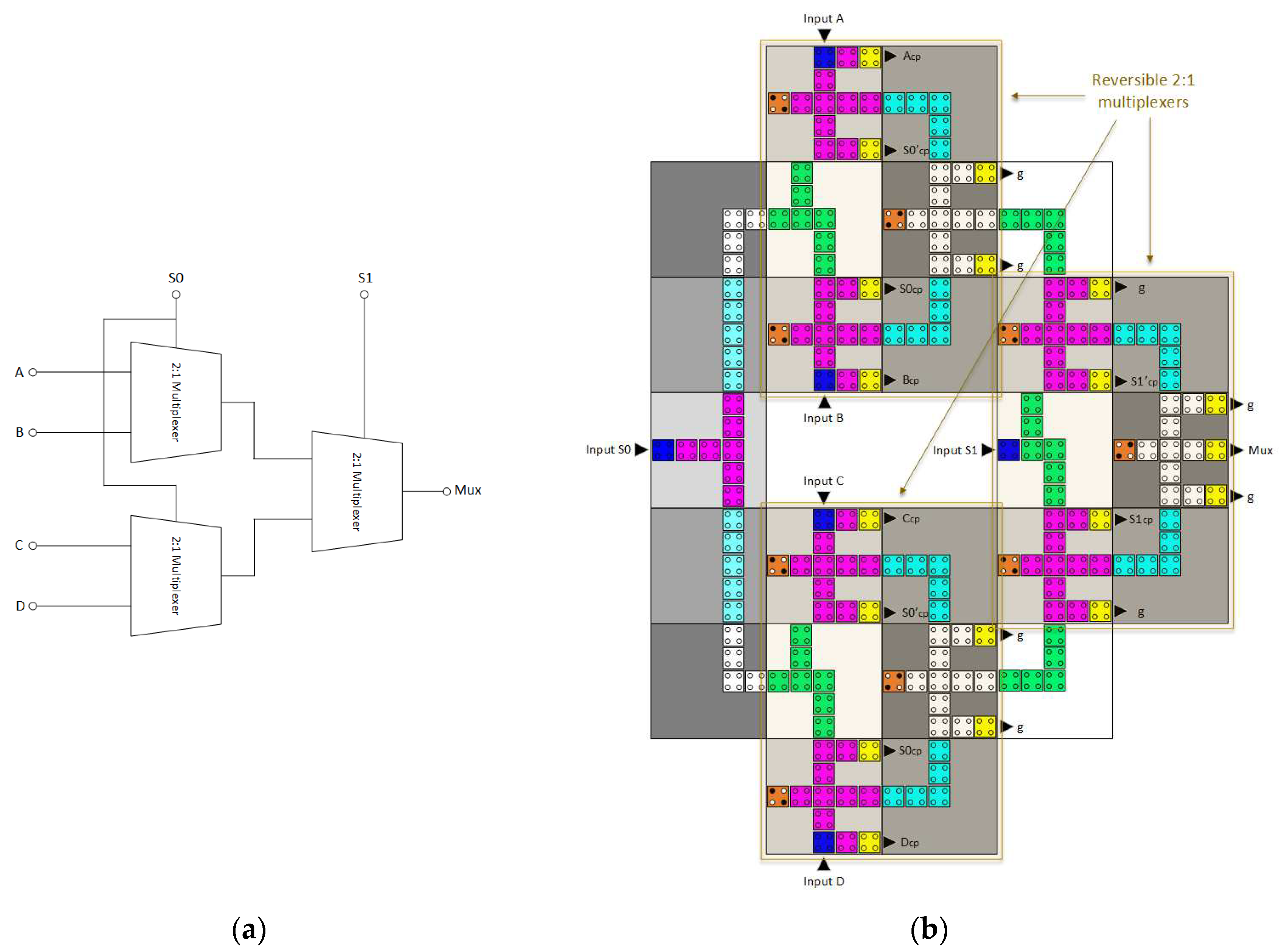
The reversible QCA 4:1 multiplexer circuit is obtained by combining three reversible QCA 2:1 multiplexer circuits, ‘connected up’ as illustrated in Figure 3. Figure 3a illustrates the synthesis of the reversible QCA 4:1 multiplexer circuit, whereas Figure 3b illustrates the QCA cell layout design. The circuit being examined incorporates an overall total of 213 QCA cells, with a total area of 0.46 µm2, employing the technology geometric parameters given in Table 1. The observed delay duration is 12 clock zones, which is equivalent to three clock cycles.
Equation 3 gives the output of the proposed 4:1 multiplexer circuit, in terms of the Boolean inputs and Table 3 displays the corresponding truth table for the circuit.
M u x = S 1 ¯ . S 0 ¯ . A + S 0 . B + S 1 . S 0 ¯ . C + S 0 . D ,

3.4. Reversible 8:1 Multiplexer

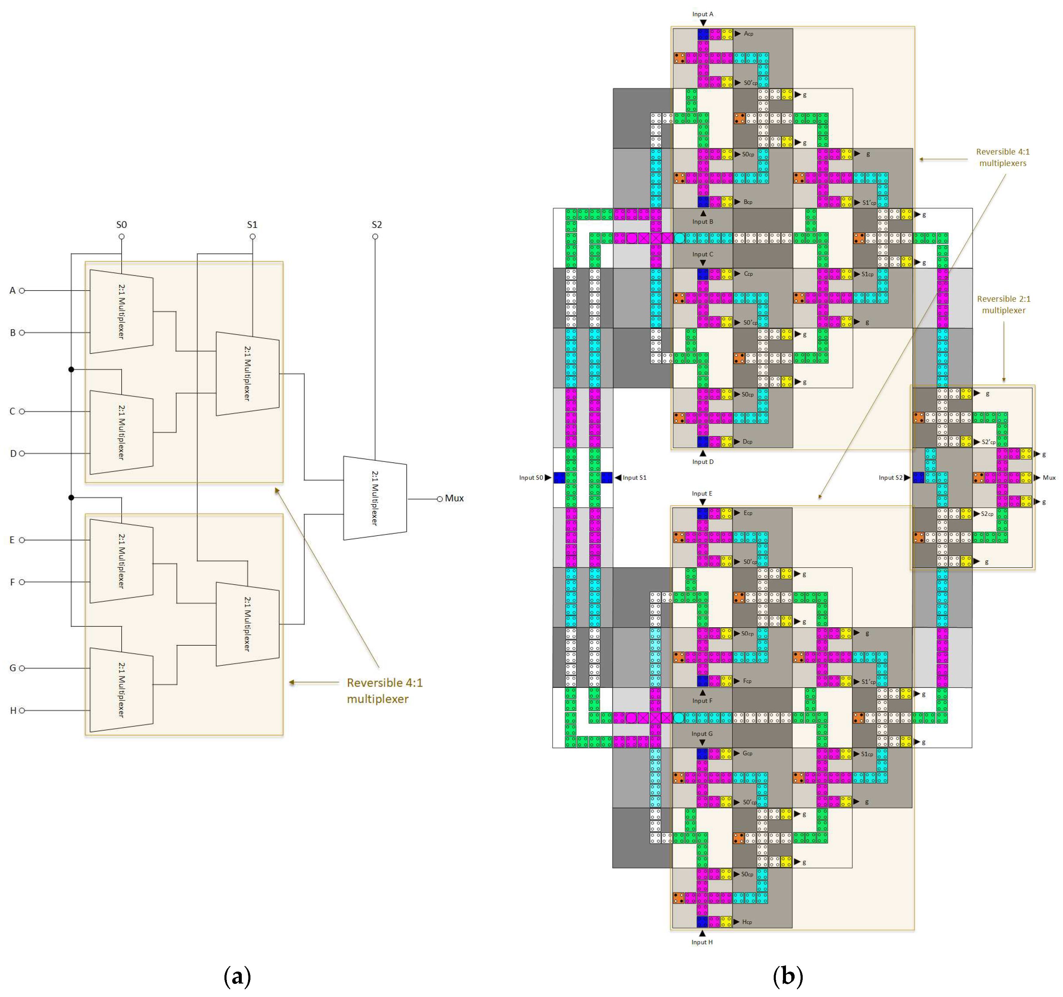
A reversible QCA 8:1 multiplexer circuit can be constructed by utilizing two reversible 4:1 multiplexers and a single 2:1 reversible multiplexers, i.e., seven reversible 2:1 multiplexers, in entirety. The hierarchical design may be divided into three distinct levels, as seen in Figure 4:
  • At the first level, a set of four 2:1 multiplexers generates four output signals, contingent upon the value of S0;
  • At the second level, two 2:1 multiplexers provides two outputs, dependent upon the value of S1;
  • At the third level, a single 2:1 multiplexer generates the final result, contingent upon the value of S2.
Figure 4a displays the synthesis process of the reversible QCA 8:1 multiplexer circuit, whereas Figure 4b displays the QCA cell layout architecture. The circuit being examined incorporates an overall total of 646 QCA cells, encompassing a total area of 1.36 µm2, when employing the technology geometric parameters given in Table 1. The observed delay duration is 22 clock zones, which is equivalent to 5.5 clock cycles.
Equation 4 denotes the output of the proposed 8:1 multiplexer circuit in terms of the Boolean inputs, and Table 4 displays the corresponding truth table for the circuit.
M u x = S 2 ¯ . S 1 ¯ . S 0 ¯ . A + S 0 . B + S 1 . S 0 ¯ . C + S 0 . D + S 2 . S 1 ¯ . S 0 ¯ . E + S 0 . F + S 1 . S 0 ¯ . G + S 0 . H

4. Energy Dissipation Simulation Results and Discussion

The energy dissipation of the proposed reversible QCA 8:1 multiplexer circuit was calculated using QCADesigner-E software version 2.2 [6], applying the technology and simulation parameters presented in Table 1. The QCADesigner-E integrates a power dissipation treatment extension into the coherence vector simulation engine (CVSE) model of the well-known QCA technology computer-aided design (TCAD) package, QCADesigner [6]. CVSE is a computational method that performs a transient analysis for the quantum mechanical density matrix microscopic description of the intra cell dynamics with the inter cell–cell electrostatic interaction incorporated within the Hartree approximation [21]. During each iteration, the CVSE calculates updated values for the coherence vector components given the time dependent tunnelling energy, determined by the clock cycle. By solving the matrix differential equations that reflects the evolution of the quantum mechanical density matrix, the coherence vector is determined. This is accomplished using an iterative fixed-timestep technique [20]. To minimize simulation errors and obtain accurate outcomes, the timestep must be sufficiently small. Presently, the time interval (Tstep) was set to 0.1 τ = 0.1 fs, with τ being the relaxation time for the dissipation model. The simulation’s error range, resulting from the implementation of this specific time step, is approximately 5%, which is within an acceptable numerical energy conservation violation.
In outline, the overall findings of the simulation results in Table 5 prove that the energy efficiency of QCA multiplexer circuits improves significantly, when a fully reversible majority gate is used as a basic building block. It is the use of the fully reversible design methodology, which preserves reversibility throughout the circuit synthesis and down to the physical layout phases, that enables the highly reduced energy dissipation. Table 5 highlights the remarkably low energy dissipation values of the proposed fully reversible designs. Each element circuit used to build the 8:1 multiplexer circuit, including the majority gate, 2:1 multiplexer, and 4:1 multiplexer, has an average energy dissipation that is lower than the Landauer energy threshold of 0.06 meV at a temperature of 1 K.
The energy efficiency of our proposed 2:1 multiplexer circuit compared with the energy values reported in the previous research literature, are presented in Table 6. The simulation for our 2:1 multiplexer circuit shows a 98% reduction in energy dissipation, compared with the previously proposed most energy-efficient 2:1 multiplexer circuit design [22]
Table 7 gives the simulation results of our new 4:1 multiplexer circuit alongside the results for the energy dissipation, from previous research endeavours. Our proposed 4:1 multiplexer circuit design exhibits a 97% increase in energy efficiency, when compared to the most energy-efficient design previously reported [22].
Table 8 displays the results of comparing the energy dissipation levels from different previous simulation studies, with our novel 8:1 multiplexer circuit. The results illustrate an 89% decrease in power consumption, compared to the most energy-efficient 8:1 multiplexer circuit design, previously proposed [22].

5. Conclusions

Reducing power consumption is a primary factor in the design of digital computer circuits for both mobile and cloud server applications. To achieve highly-energy-efficient digital computing circuits, a design approach that ensures reversibility, throughout the circuit’s synthesis and physical layout stages, must be employed. The multiplexer is a crucial basic component in many digital circuits. The primary objective of this work was to design an 8:1 multiplexer circuit, that exhibits exceptionally low power consumption. First, a novel fully reversible QCA 2:1 multiplexer circuit was devised. This fully reversible QCA 2:1 multiplexer circuit then served as the foundational building block for the development of fully reversible QCA 4:1 and 8:1 multiplexer circuits, employing hierarchical design techniques. The power dissipation was simulated using the QCADesigner-E software tool, containing a microscopic description of the QCA physics, with a treatment of the quantum mechanical mechanisms at play within a cell, the electrostatic interaction between cells and a phenomenological model of heat dissipation, to the environment. The findings of this study indicate that the fully reversible QCA 2:1, 4:1, and 8:1 multiplexers, designed and simulated in this paper, exhibit energy consumption reductions of 98%, 97%, and 89%, respectively, in comparison to the most energy-efficient multiplexer circuits proposed previously [22].

Author Contributions

All authors contributed to the study’s conception and design. Circuit design, simulation, and analysis were conducted by MA and examined by all the authors. The first draft of the manuscript was written by MA, and all authors revised the manuscript. All authors approved the final manuscript.

Funding

This research received no external funding.

Data availability statement

Not applicable.

Conflicts of Interest

The authors declare no conflicts of interest.

References

  1. Sen, B.; Sengupta, A.; Dalui, M.; Sikdar, B.K. Design of Testable Universal Logic Gate Targeting Minimum Wire-Crossings in QCA Logic Circuit. In Proceedings of the 2010 13th Euromicro Conference on Digital System Design: Architectures, Methods and Tools; 2010; pp. 613–620. [Google Scholar]
  2. Knobloch, T.; Selberherr, S.; Grasser, T. Challenges for nanoscale CMOS logic based on two-dimensional materials. Nanomaterials 2022, 12, 3548. [Google Scholar] [CrossRef]
  3. Lent, C.S.; Tougaw, P.D.; Porod, W.; Bernstein, G.H. Quantum cellular automata. Nanotechnology 1993, 4, 49. [Google Scholar] [CrossRef]
  4. DeBenedictis, E.P.; Frank, M.P.; Ganesh, N.; Anderson, N.G. A path toward ultra-low-energy computing. In Proceedings of the 2016 IEEE International Conference on Rebooting Computing (ICRC); 2016; pp. 1–8. [Google Scholar]
  5. Bennett, C.H. Logical reversibility of computation. IBM journal of Research and Development 1973, 17, 525–532. [Google Scholar] [CrossRef]
  6. Sill Torres, F.; Wille, R.; Niemann, P.; Drechsler, R. An Energy-Aware Model for the Logic Synthesis of Quantum-Dot Cellular Automata. IEEE Transactions on Computer-Aided Design of Integrated Circuits and Systems 2018, 37, 3031–3041. [Google Scholar] [CrossRef]
  7. Landauer, R. Irreversibility and heat generation in the computing process. IBM journal of research and development 1961, 5, 183–191. [Google Scholar] [CrossRef]
  8. Safaiezadeh, B.; Mahdipour, E.; Haghparast, M.; Sayedsalehi, S.; Hosseinzadeh, M. Novel design and simulation of reversible ALU in quantum dot cellular automata. The Journal of Supercomputing 2022, 78, 868–882. [Google Scholar] [CrossRef]
  9. Darji, P.G.; Makwana, J. Reversible QCA based Full-adder and Subtractor in Nanotechnology. In Proceedings of the 2022 IEEE Region 10 Symposium (TENSYMP); 2022; pp. 1–5. [Google Scholar]
  10. Naz, S.F.; Ahmed, S.; Sharma, S.; Ahmad, F.; Ajitha, D. Fredkin gate based energy efficient reversible D flip flop design in quantum dot cellular automata. Materials Today: Proceedings 2021, 46, 5248–5255. [Google Scholar] [CrossRef]
  11. Norouzi, M.; Heikalabad, S.R.; Salimzadeh, F. A reversible ALU using HNG and Ferdkin gates in QCA nanotechnology. International Journal of Circuit Theory and Applications 2020, 48, 1291–1303. [Google Scholar] [CrossRef]
  12. Torres, F.S.; Niemann, P.; Wille, R.; Drechsler, R. Near Zero-Energy Computation Using Quantum-Dot Cellular Automata. ACM Journal on Emerging Technologies in Computing Systems 2020, 16, 1–16. [Google Scholar] [CrossRef]
  13. Alharbi, M.; Edwards, G.; Stocker, R. Reversible Quantum-Dot Cellular Automata-Based Arithmetic Logic Unit. Nanomaterials 2023, 13, 2445. [Google Scholar] [CrossRef]
  14. Alharbi, M.; Edwards, G.; Stocker, R. Design and Simulation of Reversible Time-Synchronized Quantum-Dot Cellular Automata Combinational Logic Circuits with Ultralow Energy Dissipation. International Transaction Journal of Engineering, Management, & Applied Sciences & Technologies 2022, 13, 1–22. [Google Scholar] [CrossRef]
  15. Alharbi, M.; Edwards, G.; Stocker, R. Novel ultra-energy-efficient reversible designs of sequential logic quantum-dot cellular automata flip-flop circuits. The Journal of Supercomputing 2023, 1–28. [Google Scholar] [CrossRef]
  16. Pandiammal, K.; Meganathan, D. Design of 8 bit reconfigurable ALU using quantum dot cellular automata. In Proceedings of the 2018 IEEE 13th Nanotechnology Materials and Devices Conference (NMDC); 2018; pp. 1–4. [Google Scholar]
  17. Lent, C.S.; Tougaw, P.D. A device architecture for computing with quantum dots. Proceedings of the IEEE 1997, 85, 541–557. [Google Scholar] [CrossRef]
  18. Vankamamidi, V.; Ottavi, M.; Lombardi, F. Two-dimensional schemes for clocking/timing of QCA circuits. IEEE Transactions on Computer-Aided Design of Integrated Circuits and Systems 2007, 27, 34–44. [Google Scholar] [CrossRef]
  19. Campos, C.A.T.; Marciano, A.L.; Vilela Neto, O.P.; Torres, F.S. USE: A Universal, Scalable, and Efficient Clocking Scheme for QCA. IEEE Transactions on Computer-Aided Design of Integrated Circuits and Systems 2016, 35, 513–517. [Google Scholar] [CrossRef]
  20. Bajec, I.L.; Pečar, P. Two-layer synchronized ternary quantum-dot cellular automata wire crossings. Nanoscale research letters 2012, 7, 1–6. [Google Scholar] [CrossRef] [PubMed]
  21. Walus, K.; Jullien, G.A. Design tools for an emerging SoC technology: quantum-dot cellular automata. Proceedings of the IEEE 2006, 94, 1225–1244. [Google Scholar] [CrossRef]
  22. Rezai, A.; Aliakbari, D.; Karimi, A. Novel multiplexer circuit design in quantum-dot cellular automata technology. Nano Communication Networks 2023, 35, 100435. [Google Scholar] [CrossRef]
  23. Asfestani, M.N.; Heikalabad, S.R. A unique structure for the multiplexer in quantum-dot cellular automata to create a revolution in design of nanostructures. Physica B: Condensed Matter 2017, 512, 91–99. [Google Scholar] [CrossRef]
  24. Ahmadpour, S.-S.; Mosleh, M. A novel fault-tolerant multiplexer in quantum-dot cellular automata technology. The Journal of Supercomputing 2018, 74, 4696–4716. [Google Scholar] [CrossRef]
  25. Khan, A.; Mandal, S. Robust multiplexer design and analysis using quantum dot cellular automata. International Journal of Theoretical Physics 2019, 58, 719–733. [Google Scholar] [CrossRef]
  26. Jeon, J.-C. Designing nanotechnology QCA–multiplexer using majority function-based NAND for quantum computing. The Journal of Supercomputing 2021, 77, 1562–1578. [Google Scholar] [CrossRef]
  27. Khan, A.; Arya, R. Design and energy dissipation analysis of simple QCA multiplexer for nanocomputing. The Journal of Supercomputing 2022, 78, 8430–8444. [Google Scholar] [CrossRef]
  28. AlKaldy, E.; Majeed, A.H.; Zainal, M.S.; Nor, D.M. Optimum multiplexer design in quantum-dot cellular automata. arXiv preprint arXiv:2002.00360, 2020. [CrossRef]
  29. Majeed, A.H.; Alkaldy, E.; Zainal, M.S.; Navi, K.; Nor, D. Optimal design of RAM cell using novel 2: 1 multiplexer in QCA technology. Circuit world 2020, 46, 147–158. [Google Scholar] [CrossRef]
  30. Bahar, A.N.; Wahid, K.A. Design and implementation of approximate DCT architecture in quantum-dot cellular automata. IEEE Transactions on Very Large Scale Integration (VLSI) Systems 2020, 28, 2530–2539. [Google Scholar] [CrossRef]
  31. Mardiris, V.A.; Karafyllidis, I.G. Design and simulation of modular 2n to 1 quantum-dot cellular automata (QCA) multiplexers. International Journal of circuit theory and applications 2010, 38, 771–785. [Google Scholar] [CrossRef]
  32. Sen, B.; Goswami, M.; Mazumdar, S.; Sikdar, B.K. Towards modular design of reliable quantum-dot cellular automata logic circuit using multiplexers. Computers & Electrical Engineering 2015, 45, 42–54. [Google Scholar]
  33. Ahmadpour, S.-S.; Mosleh, M.; Rasouli Heikalabad, S. Efficient designs of quantum-dot cellular automata multiplexer and RAM with physical proof along with power analysis. The Journal of Supercomputing 2022, 78, 1672–1695. [Google Scholar] [CrossRef]
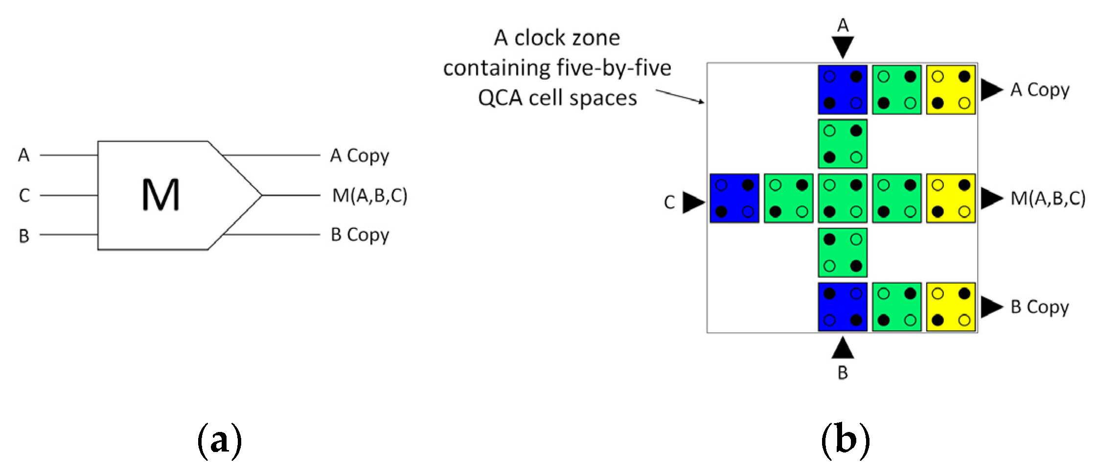
Figure 1. (a) Logical synthesis of the reversible majority gate. (b) A USE clock zone containing the physical layout of the reversible QCA majority gate.
Preprints 88483 g001
Figure 2. (a) The synthesis of the proposed reversible 2:1 multiplexer. (b) The layout of the proposed reversible 2:1 multiplexer (Acp, Bcp, Scp, and S’cp refer to copies of the input data, whereas g1 and g2 indicate the garbage outputs).
Preprints 88483 g002
Figure 3. (a) Schematic of the proposed reversible 4:1 multiplexer. (b) The layout of the proposed reversible 4:1 multiplexer (Acp, Bcp, S0cp, S1cp, S0′cp, and S1′cp refer to copies of the input data, whereas g1 and g2 indicate the garbage outputs).
Preprints 88483 g003
Figure 4. (a) Schematic of the proposed reversible 4:1 multiplexer. (b) The layout of the proposed reversible 4:1 multiplexer (Acp, Bcp, S1cp, S2cp, S1′cp, and S2′cp refer to copies of the input data, whereas g1 and g2 indicate the garbage outputs).
Preprints 88483 g004
Table 1. The technology used and simulation parameters.
Parameter Description Value
QD size Quantum-dot size 5 nm
Cell area Dimensions of each cell 18 × 18 nm
Cell distance Distance between two cells 2 nm
Layer separation Distance between QCA layers in multilayer crossing 11.5 nm
Clock high Max. saturation energy of clock signal 9.8E-22 J
Clock low Min. saturation energy of clock signal 3.8E-23 J
Relative permittivity Relative permittivity of material for QCA system (GaAs & AlGaAs) 12.9
Radius of effect Maximum distance between cells whose interaction is considered 80 nm
Temp Operating temperature 1 K
τ Relaxation time 1E-15 s
Tγ Period of the clock signal 1E-9 s
Tin Period of the input signals 1E-9 s
Tstep Time interval of each iteration step 1E-16 s
Tsim Total simulation time 8E-9 s
γshape Shape of clock signal slopes GAUSSIAN
γslope Rise and fall time of the clock signal slopes 1E-10 s
Table 2. The truth table for the 2:1 multiplexer circuit depicted in Figure 2.
S Mux
0 A
1 B
Table 3. The truth table for the 4:1 multiplexer circuit depicted in Figure 3.
S1 S0 Mux
0 0 A
0 1 B
1 0 C
1 1 D
Table 4. The truth table for the 8:1 multiplexer circuit depicted in Figure 4.
S2 S1 S0 Output
0 0 0 A
0 0 1 B
0 1 0 C
0 1 1 D
1 0 0 E
1 0 1 F
1 1 0 G
1 1 1 H
Table 5. Energy dissipation analysis of the proposed multiplexer. The average energy dissipation denotes the mean energy value averaged over the various input signal combinations.
Proposed Fully Reversible QCA Circuits Total Energy Dissipation (meV) Average Energy Dissipation (meV)
Reversible majority gate 0.009 0.002
Reversible 2:1 multiplexer 0.112 0.014
Reversible 4:1 multiplexer 0.525 0.057
Reversible 8:1 multiplexer 4.27 0.397
Table 6. Energy dissipation comparison of the 2:1 multiplexer circuit.
Proposed Reversible QCA Multiplexer Circuits Total Energy Dissipation (meV) Average Energy Dissipation (meV)
[23] 13.86 1.29
[24] 16.20 1.38
[25] 12.40 1.14
[26] 15.20 1.38
[27] 11.30 1.02
[22] 8.91 0.810
Proposed 0.112 0.014
Table 7. Energy dissipation comparison of the 4:1 multiplexer circuit.
Proposed Reversible QCA Multiplexer Circuits Total Energy Dissipation (meV) Average Energy Dissipation (meV)
[22] 17.9 1.63
[28] 19.42 2.54
[29] 27.73 4.76
[30] 97.1 15.65
Proposed 0.525 0.057
Table 8. Energy dissipation comparison of the 8:1 multiplexer circuit.
Proposed Reversible QCA Multiplexer Circuits Total Energy Dissipation (meV) Average Energy Dissipation (meV)
[23] 205 53
[22] 39.3 3.58
[31] 1110 370
[32] 700 250
[33] 108 46
Proposed 4.27 0.397
Disclaimer/Publisher’s Note: The statements, opinions and data contained in all publications are solely those of the individual author(s) and contributor(s) and not of MDPI and/or the editor(s). MDPI and/or the editor(s) disclaim responsibility for any injury to people or property resulting from any ideas, methods, instructions or products referred to in the content.
Copyright: This open access article is published under a Creative Commons CC BY 4.0 license, which permit the free download, distribution, and reuse, provided that the author and preprint are cited in any reuse.
Prerpints.org logo

Preprints.org is a free preprint server supported by MDPI in Basel, Switzerland.

Subscribe

© 2024 MDPI (Basel, Switzerland) unless otherwise stated