3.1. Dependence on annealing temperature
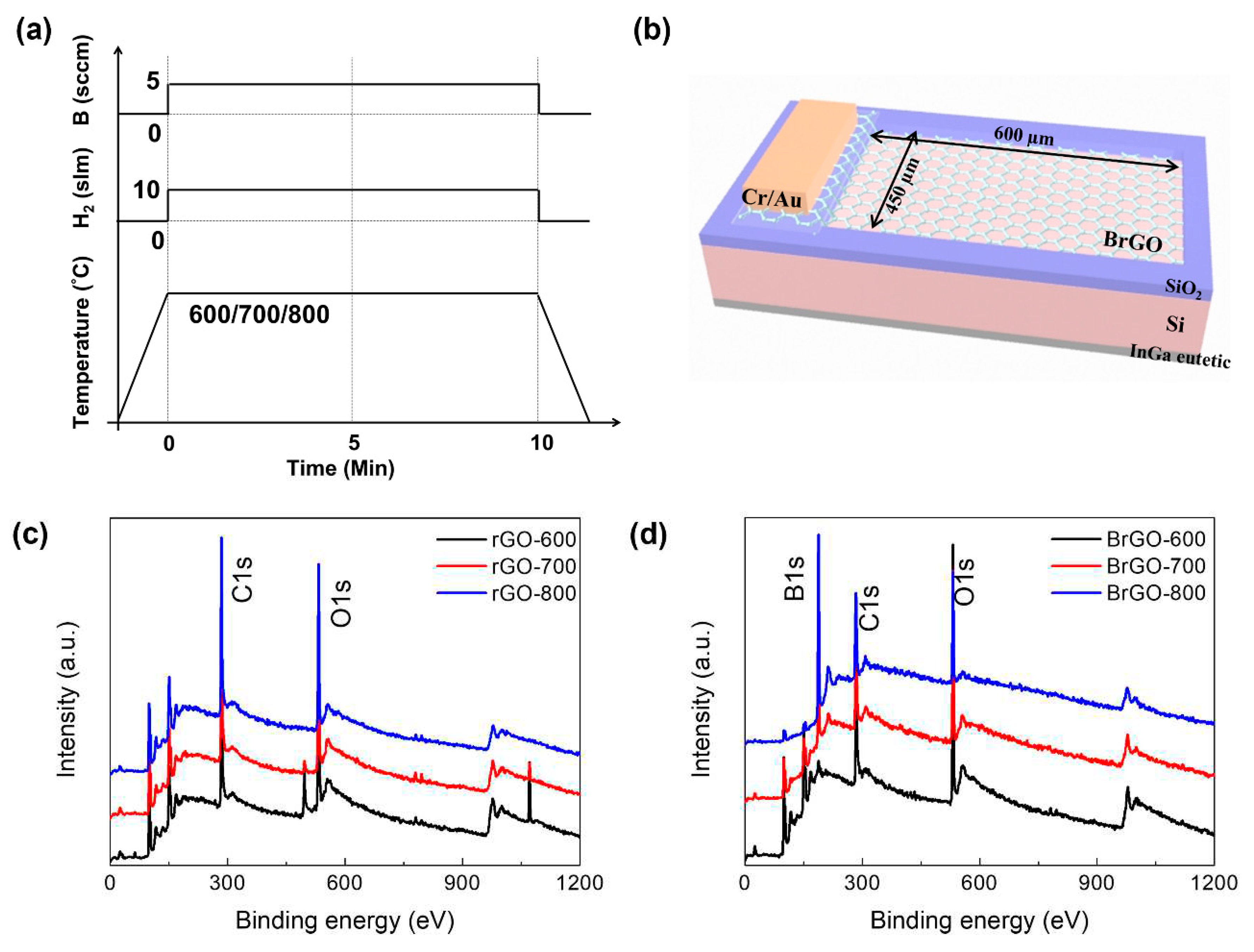
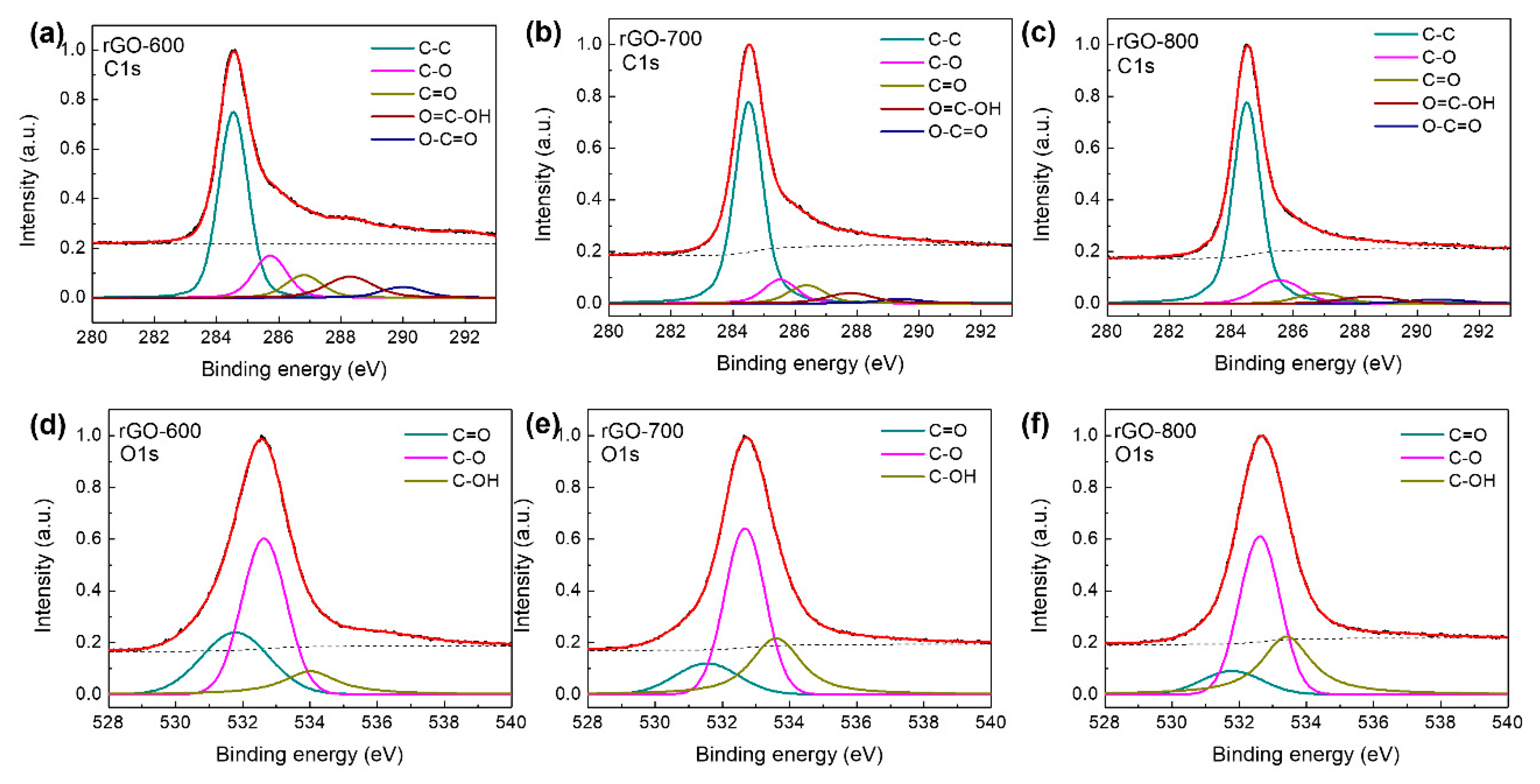
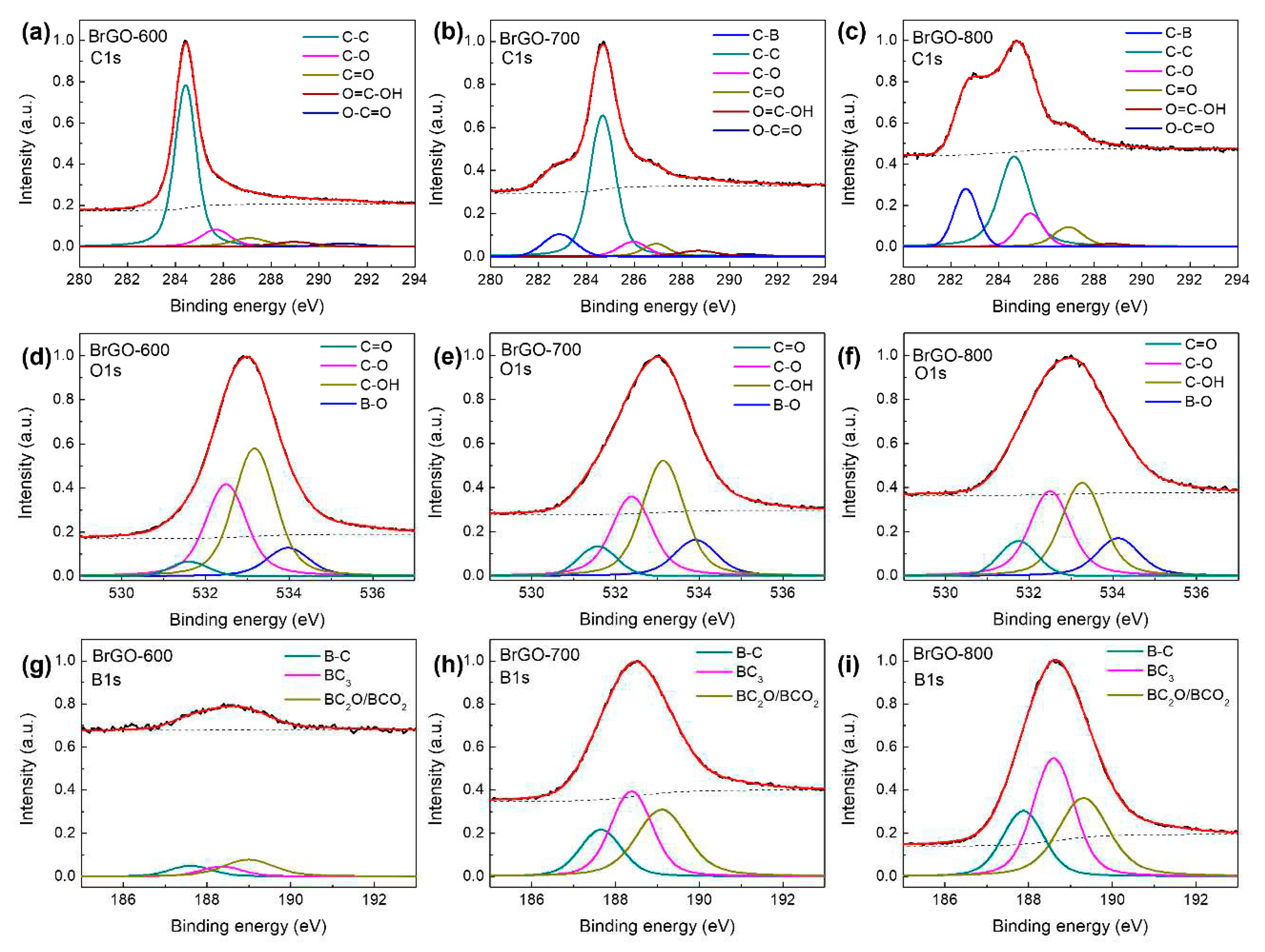
Although rGO is depicted in Fig. 1c at various annealing temperatures, the XPS spectra of B-rGO are displayed in Fig. 1d to illustrate the role of the boron dopant during the thermal reduction of rGO in the MOCVD system. The successful doping of boron atoms in the rGO crystalline network was demonstrated by the emergence of the B1s peak in the XPS spectra of the B-rGO sample. In the wide-scan spectra, the peaks at 284, 530, and 180 eV correspond to carbon, oxygen, and boron atoms. To learn more about the chemical configuration of the C, O, and B atoms in the XPS spectra, these peaks were deconvoluted and are displayed in Fig. 2 and 3. Every fitting parameter was adjusted according to the literature. The XPS C1s spectra of rGO consist of five kinds of components that are assigned to C–C (284.6 eV), C–O, or C–OH (285.6 eV), C=O (287.2 eV), O=C–OH (288.9 eV), and O–C=O (291.2 eV), as shown Fig. 2a–c [
23]. The C/O ratio of rGO samples was ~1.58 (rGO-600), 2.25 (rGO-700), and 2.98 (rGO-800), respectively. Fig. 2d–e display that the O1s peak can be fitted into three peaks at O=C (531.5 eV), O–C (532.6 eV), and C–OH (533.6 eV), respectively [
11]. The portion of C=O bonding decreased with increasing annealing temperature. The B-rGO samples exhibited an additional peak at 282.8 eV for C–B bonds due to B-doping, as shown in Fig. 3b and c [
24,
25,
26]. Agnoli et al. have reported that the boron-doped graphene material form several different functional groups ranging from substitutional boron to boronic (C=B–OH) and borinic (C–B=OH) esters, and organo-borane (C–B–H) according to the Ball model of BG [
27]. The C–B bonding portion increased with annealing temperature because of substitutional boron doping, even though the B-rGO-600 sample disappears, as shown in Fig. 3a–c. The annealing temperature increased with the reduction of the oxygen functional groups in rGO; however, the XPS C1s spectra of both B-rGO-700 and B-rGO-800 samples showed an oxygen bonding portion with a high annealing temperature owing to an increase in both boronic and borinic bonds. The XPS O1s spectra showed four-component peaks corresponding to C=O (531.6 eV) and C–O (532.4 eV), C–OH (533.2 eV), and B–O (533.9 eV), respectively, as shown in Fig. 3d–f [
26,
28]. The presence of the B–O bonding configuration in the B-rGO-600 layer indicated that there were B-doped rGO domains within the B-rGO films. The B-rGO-800 layer has a lower C-OH bonding component, which causes an increase in both boronic and borinic bonds compared to the B-rGO-700 layer. The deconvolution of the XPS B1s spectra at 187.6, 188.3, and 189.1 eV revealed the B–B, B–C, and B–O bondings, shown in Fig. 3g–i [
29,
30]. The intensity of XPS B1s peak enhances with increased annealing temperature, the B–C bonding of the B-rGO layer means that the substitutional boron dopant is attached to the rGO layer. The XPS spectra showed that the B-rGO layer was formed using the MOCVD method under the aforementioned annealing temperature conditions.
Figure 1.
(a) Schematic illustrated image of B-doped rGO with stimulate doping and annealing process, and (b) illustrated image of proposed Si/BrGO vertical structure. XPS spectra of (c) rGO and (d) BrGO with annealing temperature conditions.
Figure 1.
(a) Schematic illustrated image of B-doped rGO with stimulate doping and annealing process, and (b) illustrated image of proposed Si/BrGO vertical structure. XPS spectra of (c) rGO and (d) BrGO with annealing temperature conditions.
Figure 2.
XPS C1s spectra of (a) rGO-600, (b) rGO-700, and (c) rGO-800. XPS O1s spectra of (d) rGO-600, (e) rGO-700, and (f) rGO-800.
Figure 2.
XPS C1s spectra of (a) rGO-600, (b) rGO-700, and (c) rGO-800. XPS O1s spectra of (d) rGO-600, (e) rGO-700, and (f) rGO-800.
Figure 3.
XPS C1s spectra of (a) BrGO-600, (b) BrGO-700, and (c) BrGO-800. XPS O1s spectra of (d) BrGO-600, (e) BrGO-700, and (f) BrGO-800. XPS B1s spectra of (g) BrGO-600, (h) BrGO-700, and (i) BrGO-800.
Figure 3.
XPS C1s spectra of (a) BrGO-600, (b) BrGO-700, and (c) BrGO-800. XPS O1s spectra of (d) BrGO-600, (e) BrGO-700, and (f) BrGO-800. XPS B1s spectra of (g) BrGO-600, (h) BrGO-700, and (i) BrGO-800.
Tuning the work function of rGO materials is highly anticipated because this electrical parameter is a key factor that affects the optoelectronic device performance. The synthesis and reduction methods used, which typically result in varying aromatic sizes, defect degrees, and the number of functionalized groups on the rGO sheets, cause a significant change in the work function value [
11,
31]. Therefore, the effect of the boron dopant and the annealing temperature on the tunable work function value must be investigated.
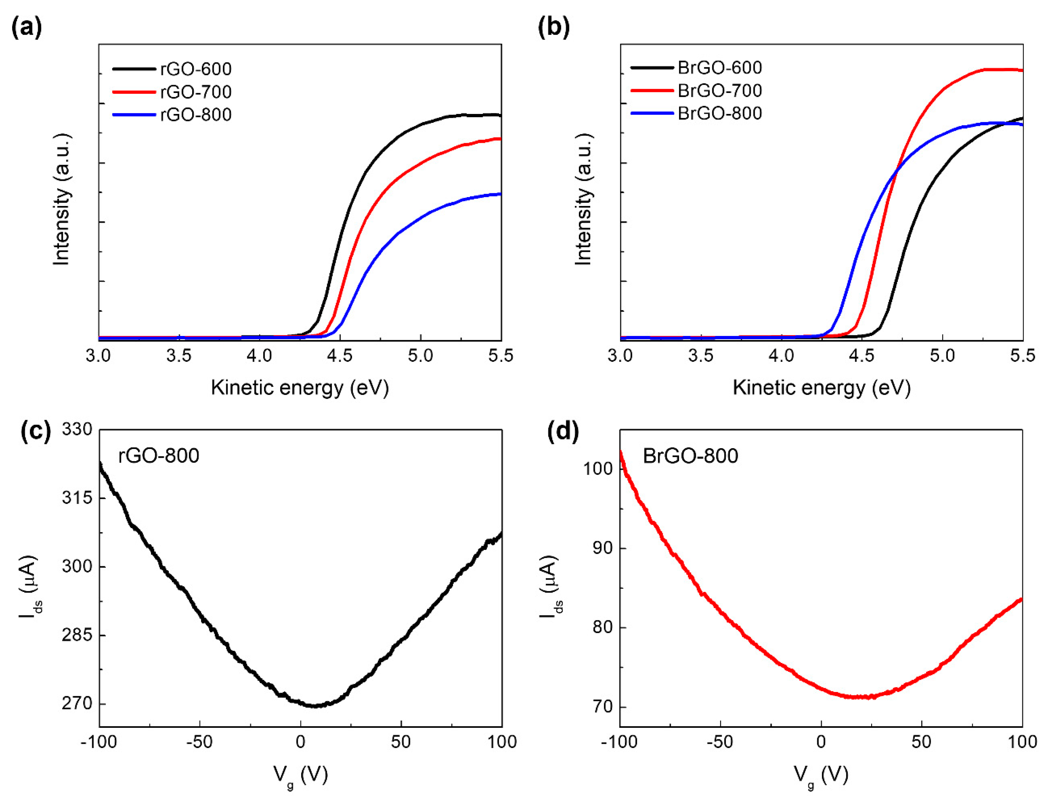
Figure 4a and b show the effect of the boron atom as well as the annealing temperature on the B-rGO layer, as determined by UPS measurements. The work function (Φ) was estimated from the empirical relation shown in Eq. 1:
where hυ, E
F, and E
cutoff are the photon energy of the incident light (21.22 eV), the Fermi level edge, and the measured secondary electron cutoff or inelastic low-kinetic-energy cutoff, respectively [
31,
32]. The E
cutoff and E
F values are obtained from UPS spectra. The work function values of the rGO samples were 4.84 (rGO-600), 4.24 (rGO-700), and 4.14 eV (rGO-800). The value of the work function decreases as the annealing temperature rises, since the higher the annealing temperature, the more oxygen functional groups are removed [
23]. Aside from that, the work function values of B-rGO samples were 5.12 (B-rGO-600), 4.95 (B-rGO-700), and 4.88 eV (B-rGO-800). Previous studies have reported that the heteroatom-doped rGO sample has a higher work function value than the rGO sample, and the work function value is dependent on the doping concentration [
33,
34]. These findings suggest that the B atoms were doped into rGO sheets to form a B-rGO layer and that the work function of the B-rGO sample is dependent on the B atom concentration.
Electrical transport measurements of rGO-800 and B-rGO-800 were performed under a vacuum to reveal the doping effect. The rGO (with and without B-doping) FET devices were fabricated with a back gate on 300 nm-thick SiO
2/Si substrates with 30/100 nm Cr/Au pads, as previously reported in the fabrication of the device [
11]. The rGO layer acts as a channel with a length of 20 µm and a width of 350 µm. The I-V characteristics were measured under vacuum conditions at approximately 1 x 10
-4 kPa.
Figure 4c and d show the drain-source current (I
ds) versus gate voltage (V
g) and the typical characteristics of rGO back-gate FETs. The voltage (V
Dirac) at the Dirac point corresponds to the minimum value of I
ds, and the Dirac point of the rGO FETs has a positive voltage for
p-type behavior. This is attributed to the oxygen functional groups in the rGO channel and the charged impurities from the SiO
2 substrate [
11]. The V
Dirac is approximately 8 V for the rGO-800 layer and 23 V for B-rGO-800, which implies
p-type behavior. The shift in the Dirac point indicates that B-doping demonstrates
p-type doping characteristics. The Fermi level in the energy band gap, which is caused by the presence of the B atom, is located at a lower level than the Dirac level. This means that the dopant caused a dipole moment on the surface of the rGO sheets [
35]. From XPS results, it is anticipated that the shifts in the Dirac point by doping were connected to the oxygen atoms attached to the B atoms. We considered both B-rGO-600 and B-rGO-700 layers to verify the
p-type characteristics, as not shown. Consequently, we believe that GO can be concurrently reduced to form rGO and doped with B using the MOCVD system, making it feasible to manufacture graphene-based optoelectronic devices on a wafer scale.
Figure 4.
UPS spectra of (a) rGO and (b) BrGO with annealing temperature conditions. Source-drain current versus gate voltage on bottom-gated field-effect transistor structure with (c) rGO-800 and (d) BrGO-800 layers measured with vacuum condition.
Figure 4.
UPS spectra of (a) rGO and (b) BrGO with annealing temperature conditions. Source-drain current versus gate voltage on bottom-gated field-effect transistor structure with (c) rGO-800 and (d) BrGO-800 layers measured with vacuum condition.
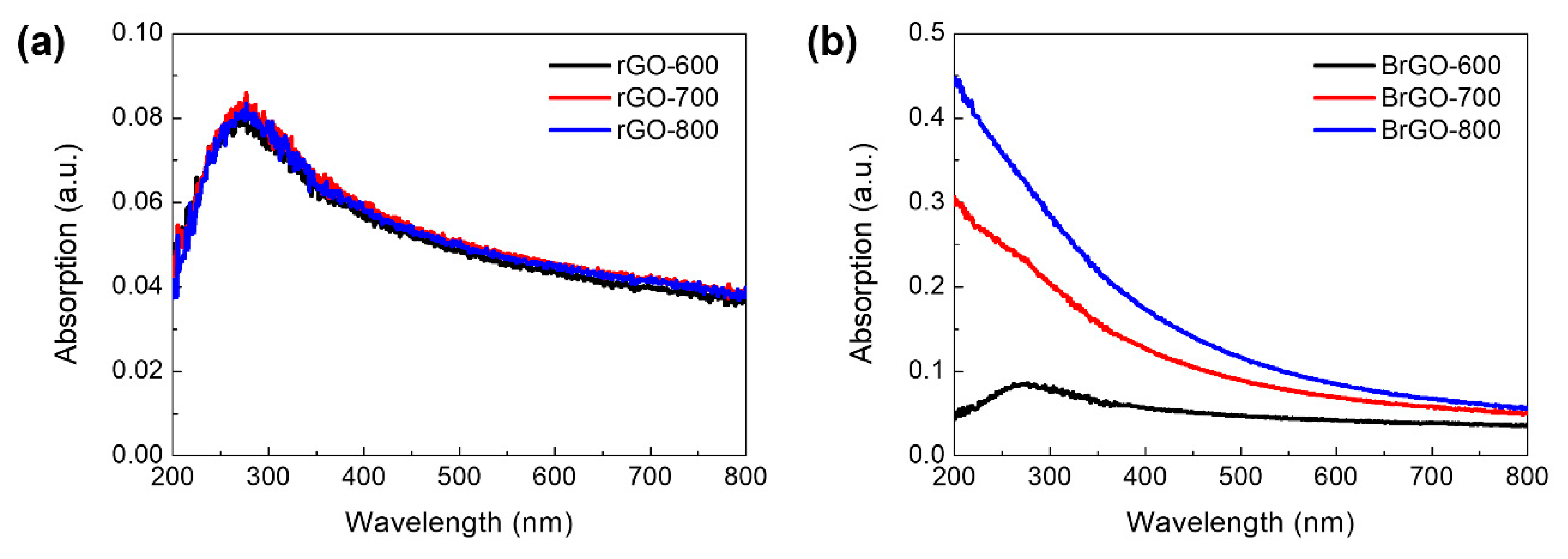
Figure 5 shows the UV-Vis absorption spectra of rGO and B-rGO at different annealing temperatures. Generally, GO exhibits a peak at approximately 200 nm, which corresponds to the π-π* transition of the sp
2 C–C bond. The peak of the rGO layer at different annealing temperatures shows a clear red shift of approximately 270 nm. The redshift is attributed to the increase in sp
2 content in the rGO with the annealing process [
19]. All rGO layers with different annealing processes have similar peak positions and absorption values. Additionally, the B-rGO samples showed an absorption peak of approximately 270 nm, which corresponds to the restoration of electronic conjugation on reduction, similar to rGO layers with different annealing temperatures. However, its absorption values are higher than those of the rGO layer [
2,
36]. B-rGO-800 did not show a peak because of the linear absorption spectra. Yang et al. reported that an increase in the doping level causes a reduction in the redshift because doped free carriers enhance the screening and consequently reduce electron-hole interactions [
37]. The linear absorption spectra in B-rGO may be linked to substitutional boron doping levels, which are correlated to the n to π* transitions in the C=B or C–B and C=O bonds. This corresponds to the electron transition from boron states to the π* states, indicating the heterogeneous distribution of boron atoms in the carbon network of the rGO sheets [
38]. Eventually, in the UV region (200–400 nm), it seems that the absorption spectra of B-rGO depended on the increased annealing temperature. A steady decrease in light absorption was observed from 400 to 800 nm, which is attributed to the minimization of sp
2 C–C domains in the B-rGO sheets. It implies that the B-rGO with a higher annealing temperature is possible to use the active layer of the PD device in the UV region.
Figure 5.
Absorption spectra of (a) rGO and (b) BrGO with annealing temperature conditions.
Figure 5.
Absorption spectra of (a) rGO and (b) BrGO with annealing temperature conditions.
3.2. Electrical Characterization of B-rGO/n-Si
Figure 6 shows the electrical properties of the rGO and B-rGO layers on
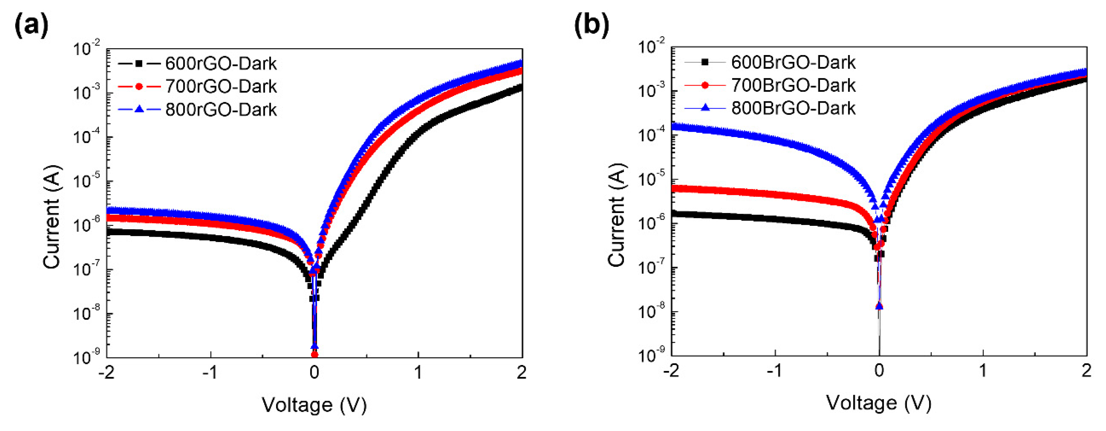
n-type Si devices annealed at different temperatures under dark conditions. The semi-logarithmic I-V curves of the rGO and B-rGO/Si diodes show Schottky behavior. The diode characteristic of the Schottky junction is described through the thermionic emission theory from dark I-V curves to verify related parameters such as the Schottky barrier height and work function [
23], as follows:
and
where I
s the saturation current, e is the electronic charge, n is the ideality factor, k is the Boltzmann constant, T is the absolute temperature, A is the active area, Φ
SBH is the Schottky barrier height, A* is the Richardson constant of Si (~112 Acm
-2K
-2). Using thermionic emission (TE) theory, the Schottky barrier height of the rGO-600, rGO-700, and rGO-800 were calculated as 0.73, 0.70, and 0.69 eV, respectively [
23]. The B-rGO/Si devices also display the Schottky junction, however, the B-rGO/Si device will become the ohmic junction with high annealing temperature (over 900
oC). The calculated Schottky barrier height of Schottky devices was 0.68 eV for B-rGO-600/Si, 0.66 eV for B-rGO-700/Si, and 0.63 eV for B-rGO-800/Si. These results indicate that the built-in electric field in the junction becomes weaker when the Schottky barrier height of the B-rGO-800/Si junction decreases with increasing doping concentration. Thus, we could anticipate the work function, which is the difference in value between the Schottky barrier height of the junction and the electron affinity of
n-Si concerning the rGO and B-rGO layers. The calculated work function values were approximately 4.78 eV for rGO-600, 4.75 eV for rGO-700, 4.74 eV for rGO-800, 4.73 eV for B-rGO-600, 4.71 eV for B-rGO-700, and 4.68 eV for B-rGO-800, as calculated using the Schottky-Mott theory. The work function values calculated from the Schottky barrier height appear to be similar to those obtained from the UPS measurements. This confirms that, as the annealing temperature increased, the work function value decreased. The elimination of oxygen functional groups and incorporation of B atoms into the rGO network were facilitated by increasing the temperature. This result demonstrates the advantages of the MOCVD method over the other approaches. We could effectively monitor the removal of oxygen functional groups that occurred simultaneously with the incorporation of B atoms into the rGO network using the MOCVD system. This opens up a new way to modulate the work function of rGO for optoelectronic device applications.
Figure 6.
I-V characteristics of (a) Si/rGO and (b) Si/BrGO devices with annealing temperature conditions.
Figure 6.
I-V characteristics of (a) Si/rGO and (b) Si/BrGO devices with annealing temperature conditions.
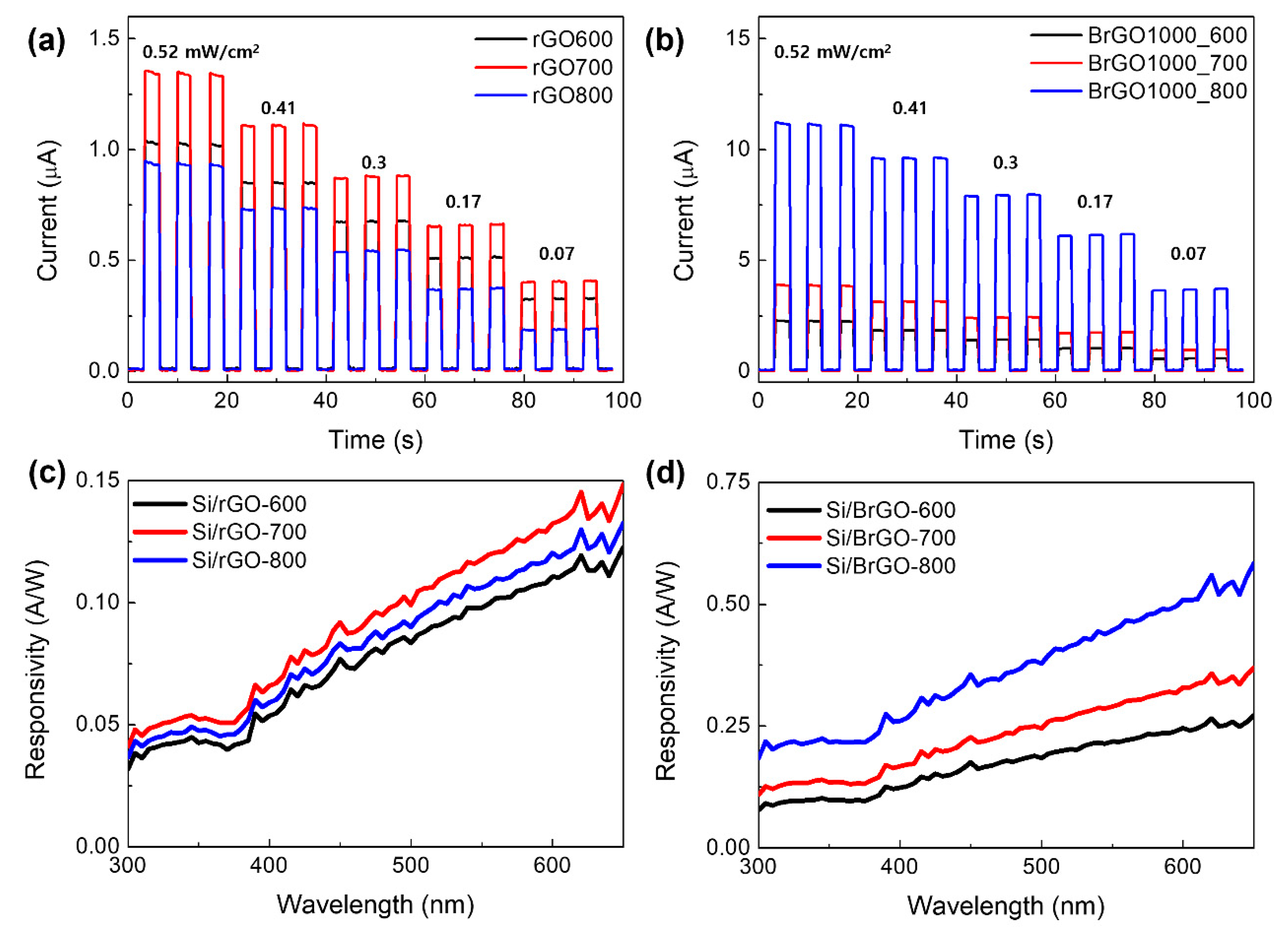
Additionally, photocurrent tests confirmed the photoresponsivity of the doped rGO samples, and the results are summarized in Fig. 7a and b. Light-emitting diodes (LEDs) with a wavelength of 385 nm were used as the illumination source. The rGO/Si heterojunction can be operated as a photovoltaic photodetector at zero bias voltage when illuminated with 385 nm light. Upon light irradiation, the photocurrent decreased with different light intensities from 0.52 to 0.07 mW/cm
2. The photoresponsive phenomenon was reversible, as shown by the immediate dissipation and recovery of the current when the light was turned off and on repeatedly. The photocurrent depends on the light source intensity. All samples exhibited fast photocurrent responses. For rGO, the photocurrent intensity decreased in the order rGO-700 > rGO-600 > rGO-800, which corresponds to Schottky behavior with a Si substrate and a decrease in oxygen functional groups. The deoxygenation of GO was responsible for the decrease in the working mechanism of the rGO layers as the annealing temperature increased. According to previous studies, when numerous oxygen functional groups are withdrawn from GO during the annealing process, the work function value of the rGO layer decreases. In general, the photoexcited carriers can be transformed into an electric current in the rGO/Si device by exploiting the built-in field that accompanies the Schottky barrier to achieve fast separation and transportation of the photogenerated electron-hole pairs. The interface between rGO and Si is well suited to delivering a relatively wide built-in potential (V
bi ~ 0.5–0.7 eV) as well as a deletion region [
39]. Therefore, it demonstrates that the holes (electrons) can be injected into the rGO layer (Si substrate) when the absorbed photons are efficiently converted into a photocurrent. Consequently, the higher work function of rGO-600 led to a smaller valence band offset between rGO-600 and the Si interface, as compared to rGO-700 [
23]. The holes could be better injected into a smaller valence band offset of the rGO-600/Si device under irradiation, while electrons could be suppressed through higher energy height in the energy band. The hole barrier probably prevents the photocurrent at the rGO-700/Si interface, and a smaller electron barrier leads to a higher I
s of rGO-700/Si in dark conditions, as compared to the rGO-600/Si device. Furthermore, the lower photocurrent values of the rGO-800/Si device imply the calculated built-in potential of the rGO-800/Si device is lower than the mentioned value of 0.5–0.7 eV. Consequently, the improved photocurrent of the rGO-700/Si device results in a lower saturation current (I
s) than those of the rGO-600/Si and rGO-800/Si devices.
Figure 7.
Time-resolved photoresponse of the (a) Si/rGO and (b) Si/BrGO devices under 385nm-UV LED illumination with variable intensity at zero bias voltage. Spectral response of the (c) Si/rGO and (d) Si/BrGO devices were obtained at zero bias voltage.
Figure 7.
Time-resolved photoresponse of the (a) Si/rGO and (b) Si/BrGO devices under 385nm-UV LED illumination with variable intensity at zero bias voltage. Spectral response of the (c) Si/rGO and (d) Si/BrGO devices were obtained at zero bias voltage.
Otherwise, the photocurrent y-axis values of rGO were 10 times lower than those of B-rGOs. The higher carrier concentration is probably due to the Hall measurement of the B-doped rGO materials. The carrier concentration value is 9.47 x 10
12 /cm
3 for rGO-600, 3.49 x 10
13 /cm
3 for rGO-700, 2.40 x 10
14 /cm
3 for rGO-800, 6.29 x 10
16 /cm
3 for B-rGO-600, 1.01 x 10
17 /cm
3 for B-rGO-700, and 3.66 x 10
17 /cm
3 for B-rGO-800. Further, the sheer resistance of rGO-600, rGO-700, rGO-800, B-rGO-600, B-rGO-700, and B-rGO-800 are 14.2 x 10
3, 10.3 x 10
3, 6.8 x 10
3, 8.2 x 10
3, 6.7 x 10
3, and 4.9 x 10
3 Ω/□, respectively. These findings indicate that the sheet resistance of the rGO layer decreased with an increase in the C/O ratio, and the properties of the B-rGO layer decreased with boron doping. It is to be noted that the photocurrent produced by the B-rGO layer was influenced by both carrier concentration and sheet resistance. The B-rGO photocurrent displayed a decreasing order of B-rGO-800, B-rGO-700, and B-rGO-600, which is coincident with the Schottky behavior of the Si substrate, the lower Schottky barrier height between the BrGO/Si interface, and the increase in B content. The origin of this photoactivity is the addition of various functional groups from the dopants [
3]. The B-rGO layer has low sheet resistance and higher carrier concentrations because of the substitutional boronic and borinic bonds in the rGO layer. Therefore, the photoexcited carriers could produce more photocurrent owing to the higher carrier concentration in the B-rGO layer. Furthermore, the interface between B-rGO and Si has a lower Schottky barrier height than the rGO/Si device, allowing photogenerated electron-hole pairs to be easily transferred to the anode/cathode. Accordingly, we assumed that the B-rGO-800/Si device could outperform the rGO-800/Si device in photocurrent efficiency.
Figure 7c and d show the spectral response of the device measured over a spectrum from 300 to 650 mn at zero bias. The responsivity values were reported by considering the proposed area given by the equation in the TE mode. The photoresponsivities of both the Si/rGO and Si/B-rGO devices increased from 300 to 700 nm. The Si/B-rGO devices have a higher responsivity over the entire spectrum than Si/rGO devices. In particular, at 400 nm, the responsivity of the Si/ B-rGO-800 device was almost five times higher than that of the Si/rGO-800 device. This is evidence of the good performance of Si/B-rGO PD devices in the UV region at 385 nm. Based on the XPS B1s spectra of B-rGO-800, we believe that the boronic and borinic bonding components, that is, the portion of B–C and B–C
3 bonding, are better than the PD performance of Si the B-rGO-800 device. Consequently, the lower work function resulted in a lower Schottky barrier height for Si/B-rGO-800. Theoretically, under UV light illumination, absorption of the incident light results in the generation of electron-hole pairs, which are quickly separated by the built-in electric field and then transferred to the electrodes. The built-in electric field at the junction interface ensures that the device can operate at zero bias voltage. Consequently, Si/B-rGO devices can enhance the photodetector performance with a tunable work function and carrier concentration of B-doped rGO at different annealing temperatures.
