Submitted:
02 November 2023
Posted:
09 November 2023
You are already at the latest version
Abstract
Two-dimensional (2D) semiconductors like Transitional Metal Dichalcogenides (TMDCs) have attracted strong research interest in the last decade. Unlike the more celebrated 2D material graphene, TMDCs like molybdenum disulfide(MoS2) possess bandgap. The number of layers critically depends on the band structure of MoS2. For example, it is indirect for bulk MoS2. However, it becomes direct bandgap material for a monolayer MoS2. Monolayer MoS2, therefore, becomes an important material for photoelectronic devices. An essential aspect of such devices is the metal-semiconductor junction. Metal-TMDC junction is, therefore, a well-studied interface due to its importance for 2D materials-based photoelectronic devices. Most importantly, it can be flexible, stretchable to it’s length, and bent to a large angle. We used metals like Au and Al to interface with TMDs like MoS2. We used silicon and PDMS as substrates. So, we have to focus on investigating the relative properties of various TMDCs. We see change in band energy and vibrational modes via Photoluminiscence and Raman spectroscopy as shown in the article. However, certain aspects are yet to be explored, for example, how this interface behaves in the presence of strain.
Keywords:
Metal_2D semiconductor interface
; 2D semiconductor material
; Raman and Photoluminescence Spectroscopy
1. Introduction
Transition Metal Dichalcogenides (TMDCs) are considered promising for the next generation of nano-electronics due to their unique properties. In particular, their high surface-to-volume ratio and atomically thin structure make TMDC-based devices highly desirable Exploring the properties of these devices, especially concerning the charge injection and charge carrier trapping at the dielectric/TMDC interface, is of great importance. Current semiconductor technology relies heavily on silicon and group semiconductors, owing to their distinct properties, such as their ability to conduct electricity under certain conditions and act as insulators under others [1]. Doping processes can further enhance their electrical properties, making them ideal for amplifying electrical signals. Moreover, the abundance of silicon on Earth contributes to its widespread use in electronic devices [2,3].
While silicon has been a predominant material for electronic devices, other materials have gained attention, including graphene and Transition Metal Dichalcogenides (TMDCs). Graphene, with its exceptional properties such as high mobility, flexibility, and electrical conductivity, shows promise as a potential alternative to silicon. TMDCs, in particular, are gaining prominence due to their unique two-dimensional properties and functionalities, especially in flexible optoelectronic devices. Of these, Molybdenum Disulfide (), a type of TMDC, has garnered significant attention. Its monolayer structure, with a direct band gap of eV, makes it suitable for various applications such as photodetectors, transistors, and LEDs [4].
Understanding the structural and optical properties of is essential. Raman and photoluminescence spectroscopy play crucial roles in this regard [5]. Raman spectroscopy allows the analysis of vibrational energy modes, while photoluminescence spectroscopy provides insights into the material’s internal properties and interface characteristics that are not accessible through other means. These techniques aid in comprehending the energy band structure and excitonic properties of . Additionally, the study investigates the optical properties of the 2D semiconductor-metal interface, shedding light on the underlying physics and potential applications of these materials [6].
This simplified version captures the essential aspects of the study, highlighting the significance of TMDCs, particularly , and their properties in the context of electronic devices and nano-electronics.
Semiconductors are crucial in our modern lives, serving as essential materials for various devices. Understanding their fundamental electronic properties is key to leveraging their potential. The semiconductor’s distinctive characteristic lies in its response to an applied electric field. The concept of the bandgap is fundamental in this context, where molecular orbitals form two energy bands - the bonding-orbital or valance band, and the antibonding-orbital or conduction band [7]. In these bands, the energy levels tend to smear, allowing continuous observation. For electrons to move from the valance to the conduction band, they need energy greater than the bandgap. In contrast, metals possess different electronic distribution, enabling immediate energy absorption from an applied electric field due to the presence of empty energy states [8].
- Parameters for Metal-Semiconductor Interface.
Understanding electronic material parameters is crucial for comprehending the metal-semiconductor interface. Parameters such as the fermi level (), vacuum level (), work function , energy gap (), ionization energy (IE), and electron affinity (EA or) play a significant role in controlling charge exchange and transport across various interfaces in electronic devices. The Fermi energy level (Ef) represents the energy difference between the highest and lowest occupied particle states. Similarly, the work function symbolizes the minimum amount of thermodynamic work required to remove an electron from the material to the vacuum level. This understanding is depicted in the energy diagram, providing insights into the material’s electron behavior and the charge carriers within the semiconductor.
Figure 1.
Shows the Excitation of an electron to a higher energy level and the subsequent de-excitation that gives out A and B exciton.
Figure 1.
Shows the Excitation of an electron to a higher energy level and the subsequent de-excitation that gives out A and B exciton.
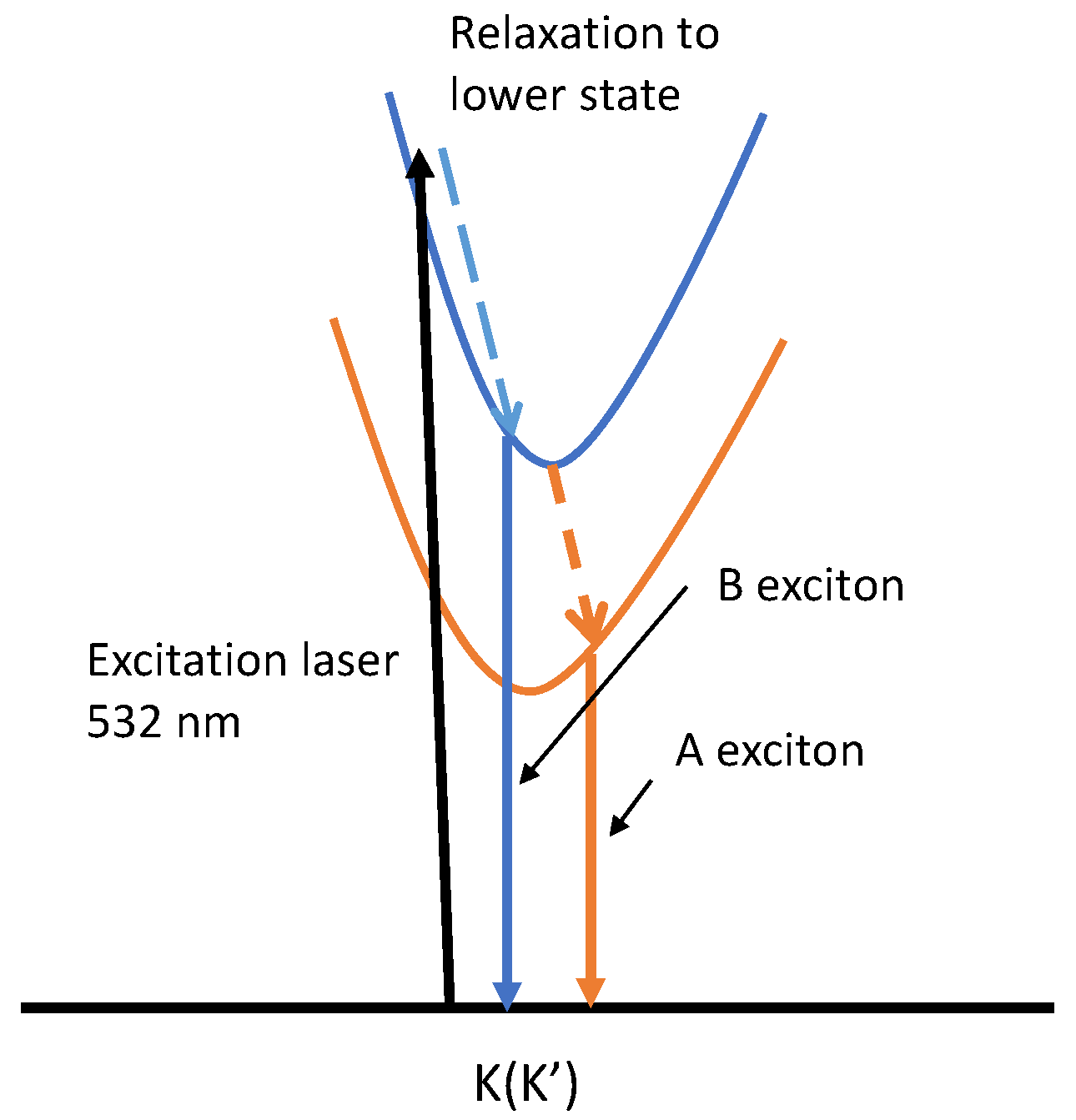
In the world of 2D semiconductor devices, the 2D semiconductor-metal contact holds significant importance. Metal-semiconductor contact leads to two types of contact widely used in semiconductors: the Schottky barrier contact and the Ohmic contact. The formation of these contacts depends on the difference in fermi energies during the contact. Under ideal conditions, the metal and semiconductor are assumed to be in direct contact without any oxide or charge layer at the atomic level. No intermixing or interdiffusion takes place during this contact. The Schottky barrier contact forms a large potential barrier when the fermi energies of the metal align together, resulting in rectifying characteristics suitable for use as a diode shown in Figure .
Figure 2.
shows the metal-semiconductor after contact at the non-equilibrium condition when we have metal work function greater than semiconductor work function ( > ) and vice versa < .
Figure 2.
shows the metal-semiconductor after contact at the non-equilibrium condition when we have metal work function greater than semiconductor work function ( > ) and vice versa < .
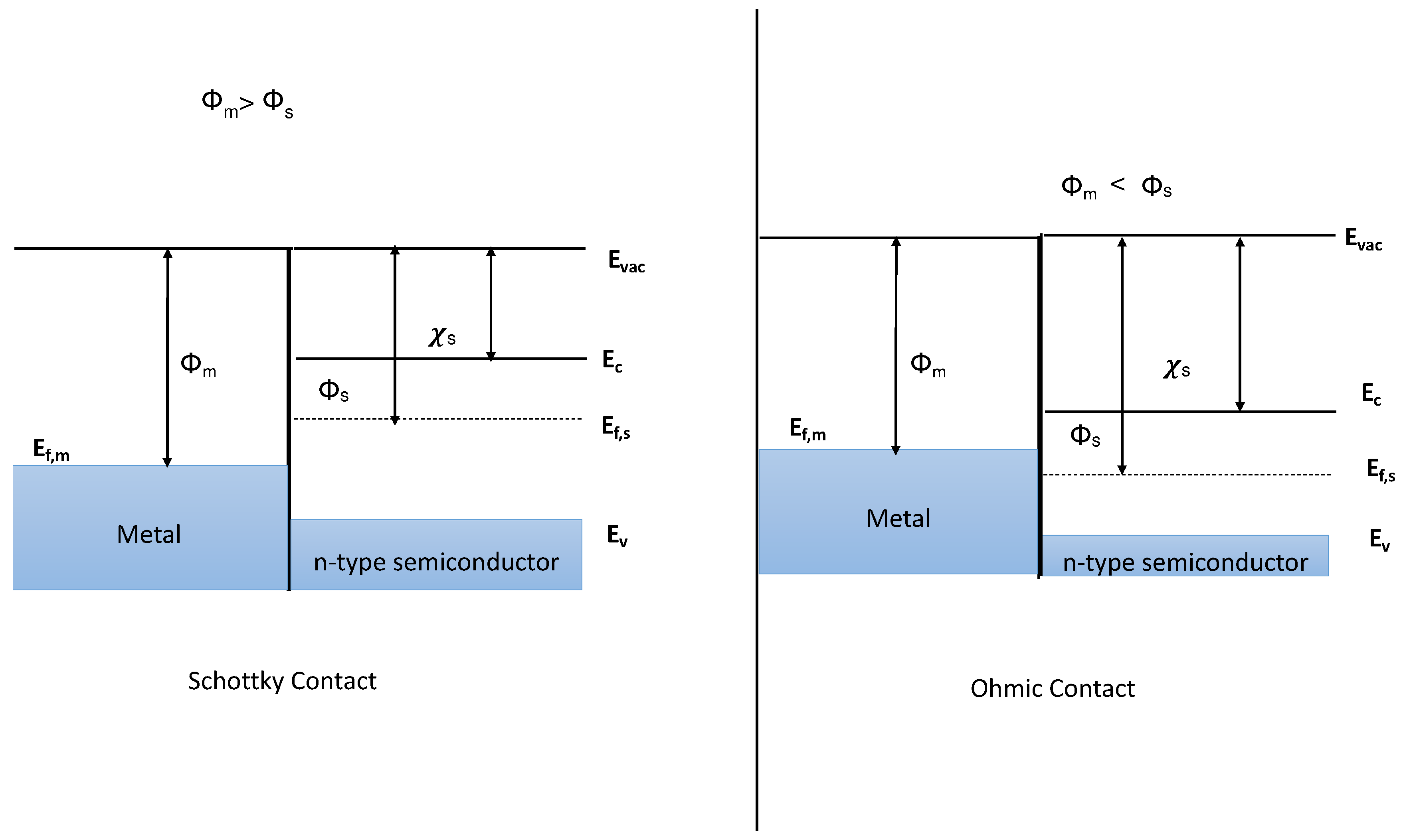
On the other hand, the ohmic contact allows current flow in both directions, displaying no potential height barrier between the 2D semiconductor and metal interface. The band banding concept illustrates the behaviour of the free charge carriers within the materials, allowing a better understanding of their electronic structure. The I-V characteristics of both types of contacts display distinct patterns under different biasing conditions, aiding in comprehending the flow of electrons in these contacts [9].
2. Formation of 2D Semiconductor-Metal Interface
Before we prepare the sample of 2D semiconductor metal, we have to know how we can transfer the semiconductor material flake to the desired substrate.
flake transfer
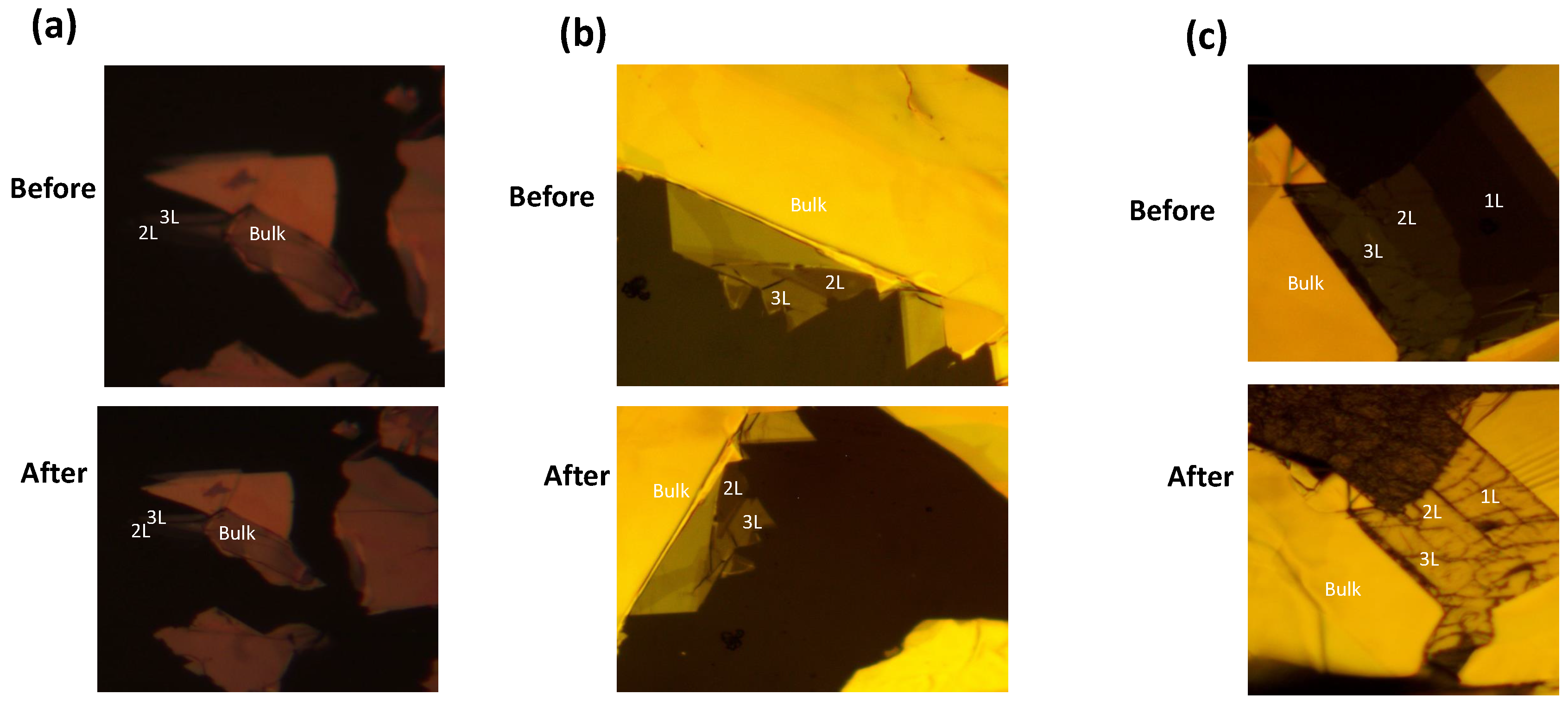
First, we have to know how to transfer the flake and get a monolayer to multiple layers. A micromechanical exfoliation of 2D crystals method is also known as the "Scotch tape method" discovered by Andre Geim and Konstantin Novoselov. This is a common technique to transfer the flake of on the substrate at the nano scale. We have to follow the steps to prepare the flake.Take the semiconductor material, in our case . By using the tweezer, take a small piece of and put it on the adhesive tape. The tape with crystals of layered material is pressed against the surface of choice on the substrate.upon peeling off, Some of the crystal’s bottom layer is left on the substrate. Now see the transferred flake under the microscope to identify the monolayer or multiple layers of flake .The steps we are followed are shown in Figure 3.
3. Raman and Photoluminescence of Different layers of and experimental setup
After transferring the flake onto the substrate, we must identify the monolayer under the microscope. For this, we use the and lenses and try to identify, by using contras, the layer thickness to the background substrate as seen in Figure 3(d).
After the process of flake deposition, we move on to the following setup of performing the measurements. For this, we work with the Raman spectroscopy (backscattering) setup. It contains the excitation laser, followed by a laser line filter which allows the only laser to pass through and clean it spectrally. When we see the schematic diagram of the setup (see Figure 4 (b)) in the following line, we have a beam splitter, which directs the incident light towards the substrate (PDMS or Si).
However, before entering the light into the spectrometer, a notch filter is also added to block the laser signal and only allow the signal to come from the sample. A white light source is added to locate the monolayer by using different objective lenses on the substrate and with the help of a Thor-labs camera. Images of these flakes are also shown in Figure 7. All the data presented here is taken on these flakes using the setup described below
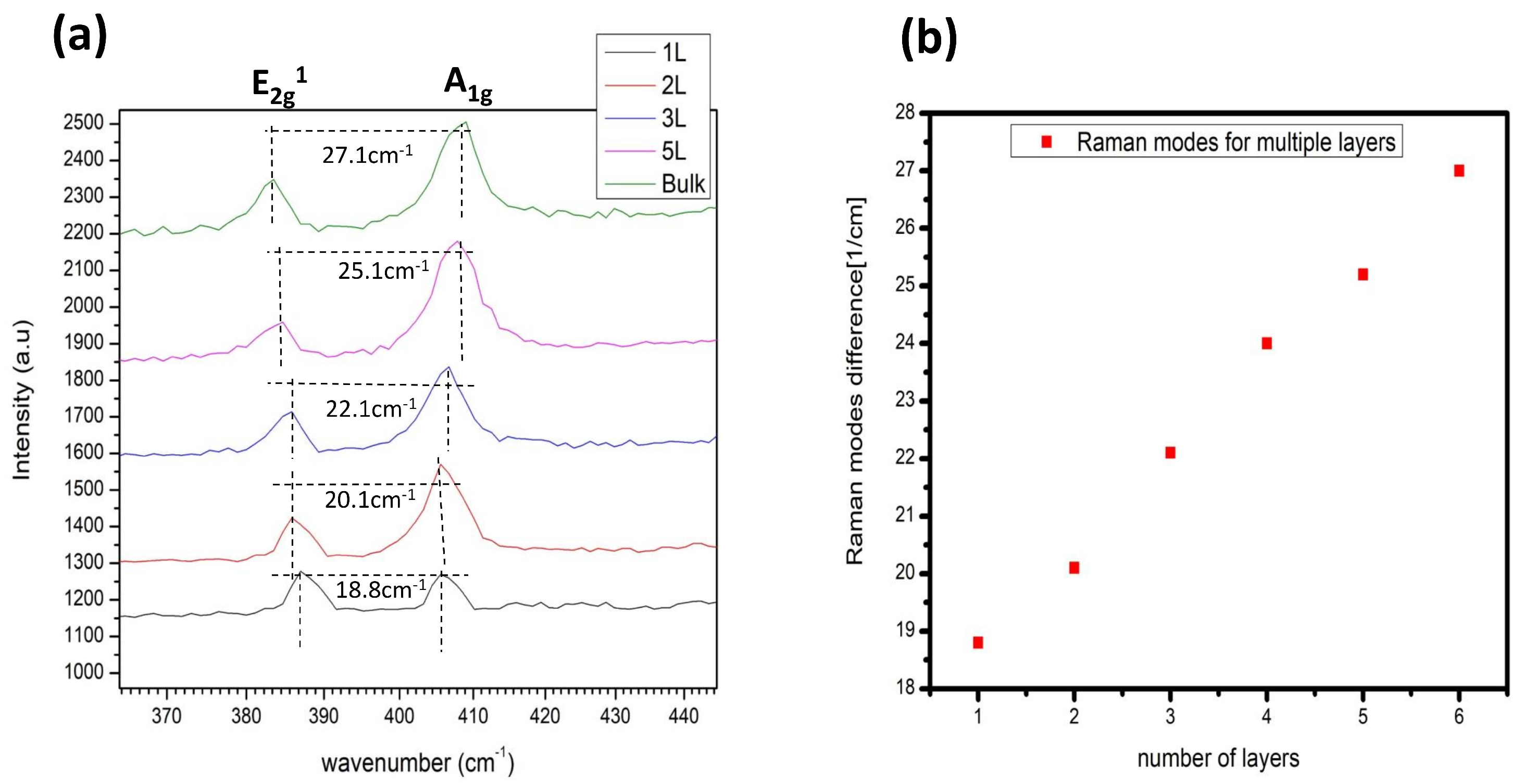
The Raman characterization of the prepared sample went through the setup, and a wavelength laser was used to characterize the flake. We end with the results that the monolayer shows the Raman active mode and with spectral separation of (see Figure 5(a)). The spectral separation in the vibrational modes happened by increasing the number of layers. We can conclude that by increasing the number later, the separation within modes increases because of the change in interlayer interaction, and the bond lengths also change (see Figure 5(b)). We can discuss the photoluminescence spectroscopy of that happens to optical PL to Monolayer when we increase the number of layers of. About the optical characterization of monolayer . Here we will see PL characterization for the different layers.
In the monolayer case, the peak intensity corresponds to A exciton at . However, the excitonic energies depend upon the number of layers, and the peak intensity of these peaks depends upon the interlayer coupling. By increasing the number of layers toward bulk, the intensity goes down, and the peaks go shift towards the left. As the number of layers increases, goes from direct to indirect bandgap semiconductor and emission intensity decreases due to phonon-assisted relaxation requirement. Because of this reason, the peak also shifts towards lower energy (eV). So, we can conclude that by increasing the number of layers, the PL intensity decreases, and the peak shifts towards lower energy (eV).
Figure 4.
(a) microscopic picture of flake with different number of layers. (b) schematic diagram shows the Raman and photoluminescence set up along with the white light source, Which is used to locate target area on the substrate.
Figure 4.
(a) microscopic picture of flake with different number of layers. (b) schematic diagram shows the Raman and photoluminescence set up along with the white light source, Which is used to locate target area on the substrate.
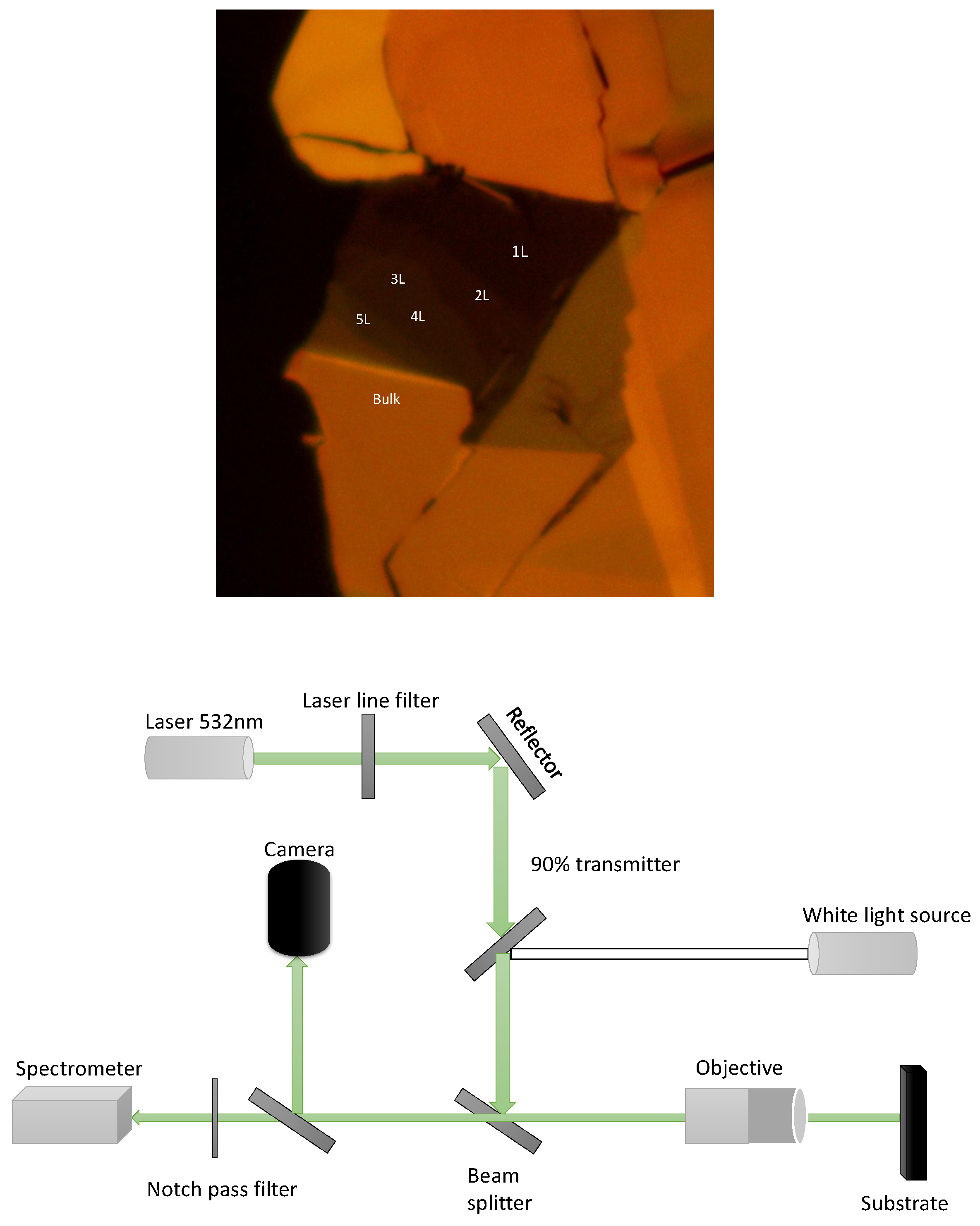
Figure 5.
(a) Raman spectra of the monolayer, bilayer to bulk (b) By increasing the number of layers, the Raman modes separation increases.
Figure 5.
(a) Raman spectra of the monolayer, bilayer to bulk (b) By increasing the number of layers, the Raman modes separation increases.
4. Sample Preparation of 2D Semiconductor-Metal
We discussed already above how we can transfer flake on the substrate. It will be easy for us to understand sample preparation in a sequence. To prepare the sample of the Metal-semiconductor interface, we have different metals and as a 2D semiconductor. When we make contact, then the flow of electrons will happen to attain the equilibrium. In this section, we focus on the preparation of the Metal-semiconductor interface, for we should have hard card tape, double-sided tape, and use Polydimethylsiloxane (PDMS)/ Silicon (Si) as a substrate and thin layer of metal which we have to deposit on the flake at the end by using physical vapor deposition (PVD) or magnetron sputtering.
Figure 6.
schematic diagram of the metal-semiconductor interface (a)Metal- contact and next prepared sample of thin metal film on flake on PDMS as a substrate (b)Metal- contact and next prepared sample of thin metal film on flake on silicon as a substrate (c) PVD method which used to deposit the thin film on flake.
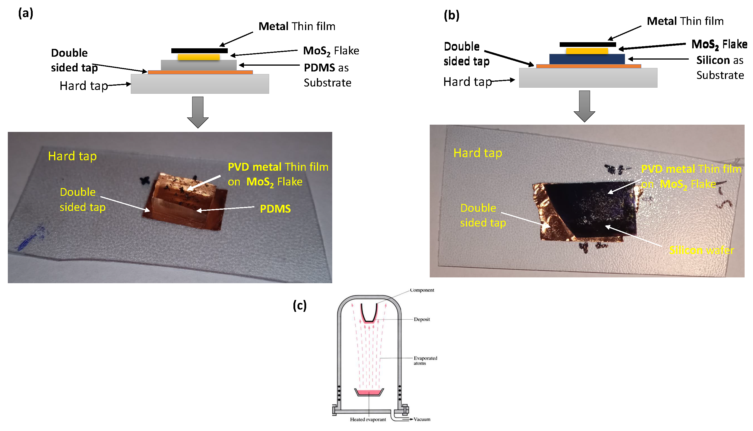
PVD processes are sputtering and evaporation. This method is also used to manufacture thin films for optical, mechanical, chemical, and electronic functions. In our case, we will use both for the deposition of metals on substrates.
For sample preparation, we must follow the steps discussed, take hard card tape (flexible tape), put a piece of double side tape on it, and stick the wafer of silicon or PDMS (in our case, we use both one by one). We have to transfer the flake onto the desired substrate. The process of transferring the flake is already discussed in the above section, and at the end, deposition of a thin film of metal onto the transferred flake by using PVD or magnetron sputtering.
5. Deposition of different Metals on flake
This section will see microscopic pictures of different Metals on the flakes. By contrast, we can make a difference between before and after deposition. First, we use the metal gold having a thickness of 5nm deposited on bilayer by using magnetron sputtering. See Figure 7 (a). You can see the microscopic picture under 50x before and after the deposition of gold. Figure 7 (b) shows the growth of aluminum with a thickness of 1nm before and after deposition on bilayer flake. In Figure 7(c), you can see the clear difference before and after the growth of silver, having a thickness of 2.5 nm. You can see the single layer, bilayer to the bulk of the MoS2 flake. All these prepared samples are studied under the microscope (50x) and use the PDMS as a substrate.
Figure 7.
(a)Au- 2L Contact With 5nm Gold thickness.(b) Al- Contact With 1nm Aluminium thickness. (c) Ag- Contact With 2.5nm Silver thickness.
Figure 7.
(a)Au- 2L Contact With 5nm Gold thickness.(b) Al- Contact With 1nm Aluminium thickness. (c) Ag- Contact With 2.5nm Silver thickness.
6. Results and discussion
Photoluminescence Spectroscopy of gold and aluminum on (Metal- interface)
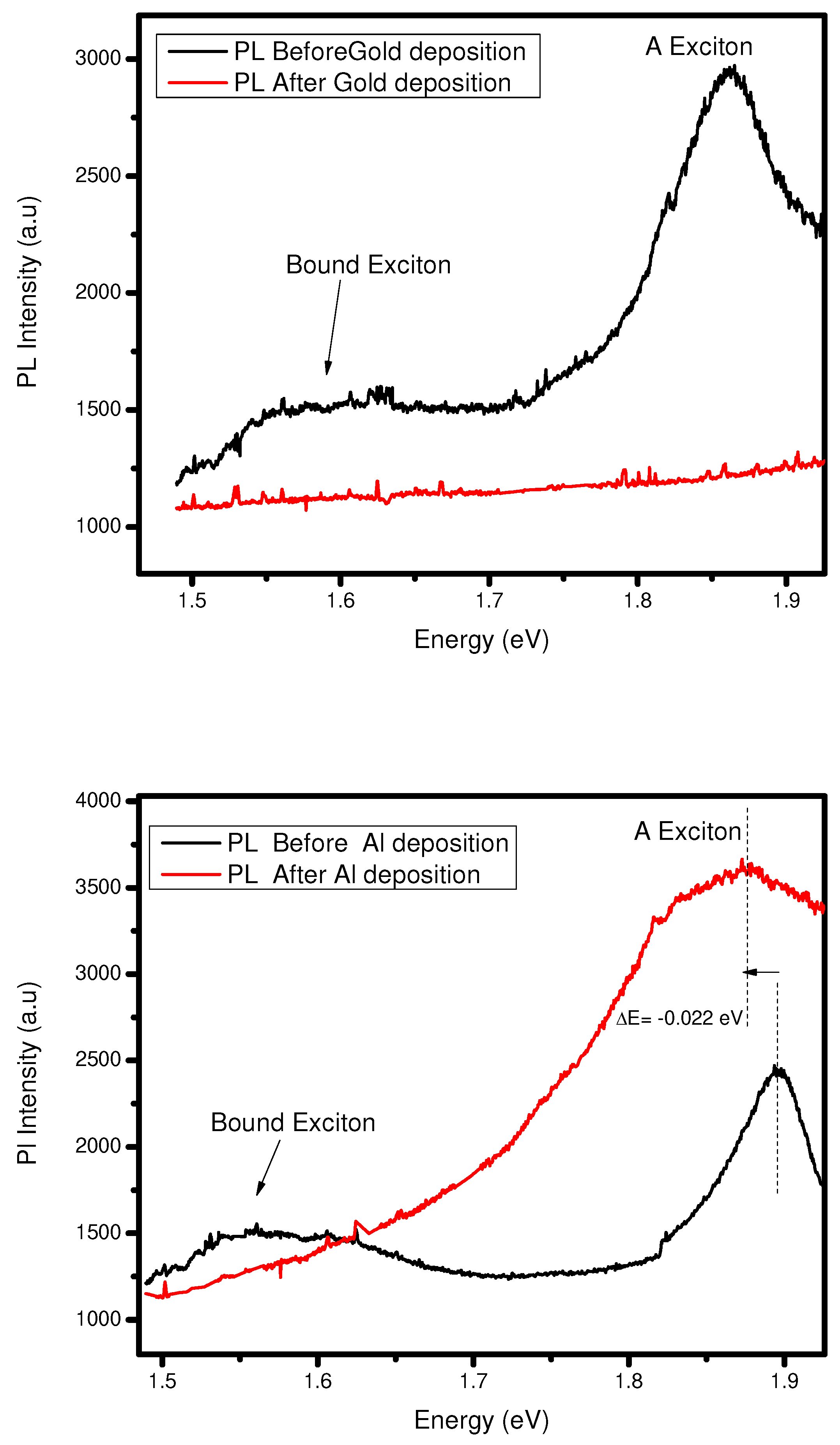
In this section, we will see the optical properties for deposition of gold and aluminum on , respectively. First, we sputter the gold of 5nm thickness on the flake. Gold has a work function of eV, and bilayer has eV. According to the work function and literature view, they make the Schottky contact. If we see in Figure 8 (a), the PL get quench clearly and has no A exciton or bound exciton because they make a Schottky contact. The work function of gold is greater than the work function bilayer . So, more electrons are moved from semiconductors to metal, and we know that metal has no bandgap. The metal shows no photoluminescence, and the PL intensity goes down due to most of the electron movement from semiconductor to metal.
In the case of aluminum, if we deposit the Al of 1nm thickness by using PVD on the bilayer. The photoluminescence increases three times (see Figure 8(b)). The work function of aluminum is eV, which is less than bilayer . So, they make an ohmic contact in which we can say that most of the electrons move from metal to semiconductors. The bilayer already has a bandgap of 1.8 eV, and electrons also come from the metal. So, we can conclude that due to this type of electron movement, the photoluminescence of Al- increases three times, and the peak shift from eV to eV. Because of the Al conduction on , the peak shifts and the bandgap of Al- go from direct to indirect because we see the decrease in the bandgap energy in this case.
Figure 8.
(a) PL before and after megnetron sputtering of 5nm gold on bilayer and PMDS as substrate .(b) PL before and PVD of 1nm Al on bilayer and PDMS as substrate .
Figure 8.
(a) PL before and after megnetron sputtering of 5nm gold on bilayer and PMDS as substrate .(b) PL before and PVD of 1nm Al on bilayer and PDMS as substrate .
6.1. Raman Spectroscopy of gold and aluminum with
For the case of Raman spectroscopy, we already discuss that after sputtering of 5nm gold and deposition of 1nm Al on bilayer , what kind of contact they form. In the case of gold, If we see the Raman vibrational modes and before and after the sputtering of gold, we find no Raman modes shifting. That means nothing happened to the vibrations of phonon in the Au- contact (see Figure 9(a)).
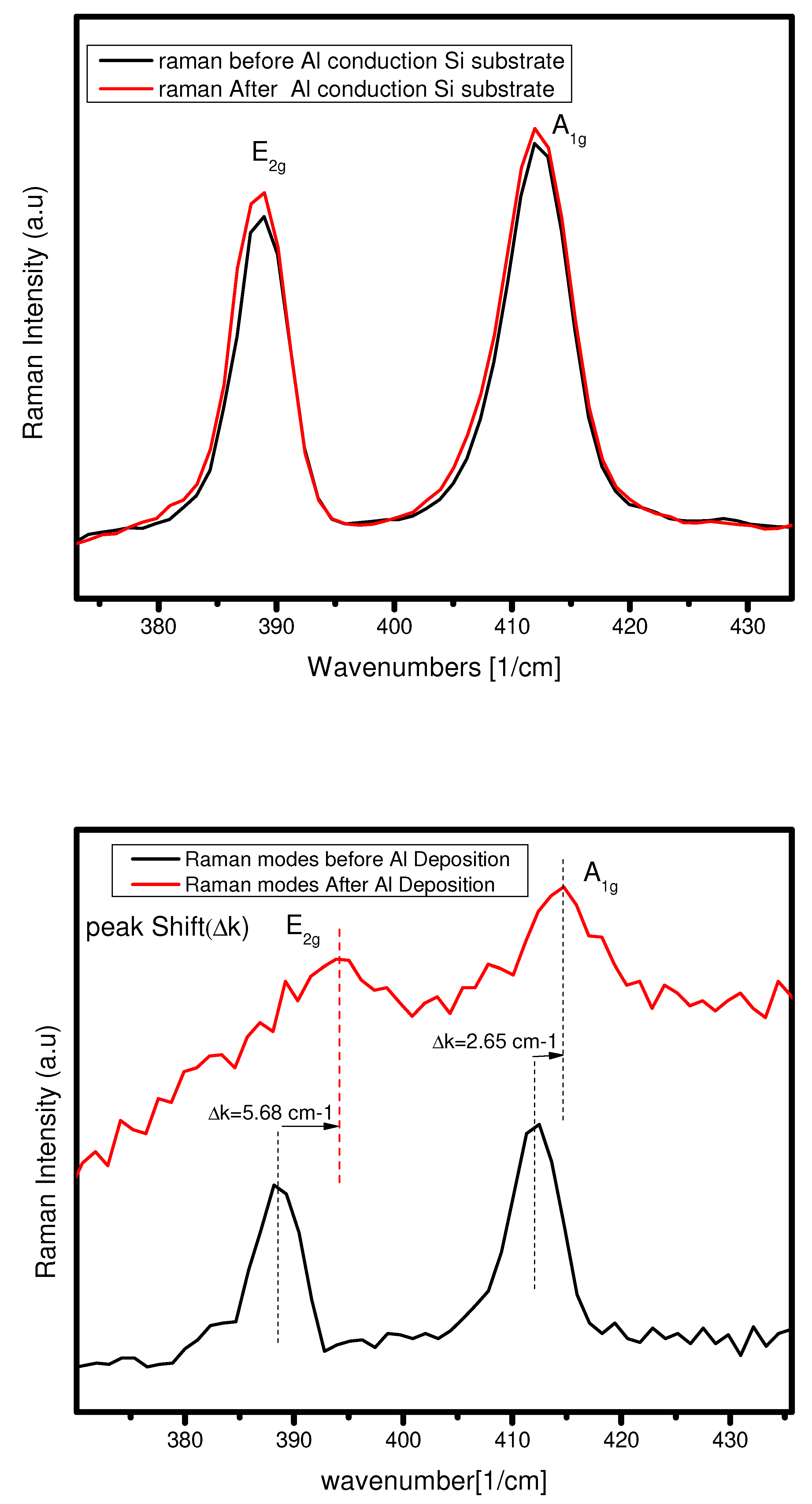
Nevertheless, in the case of Al on 2L , there are shifting of in-plan vibration and in out-plan vibration. The vibrational mode shifts from 388.54 to 394.01 and A1g mode shifts from 412.09 to 414.75 . So in, the has more shifting than the corresponding mode. This means that phonon’s in-plan vibrations are more disturbed by the Al conduction on bilayer , and in out-plan vibration has less disturbance due to the conduction (see Figure 9(b)). We can see that the vibrational mode for Al- is not so clear because having disturbance due to IPA (cleaning agent) on the surface of the substrate. So, make sure that the IPA is cleaned out before using the sample for optical characterization.
Effect of substrate
The role of the substrate is also essential in understanding the optical characteristics of metal-semiconductor contact. The optical properties are changed by changing the substrate. We use two kinds of substrate PDMS and silicon. The PDMS is a flexible substrate having a high-quality property of high mechanical strength, high transparency, thermally stable at room temperature, and high optical properties [11]. On the other hand, silicon is an ideal substrate for exploring the microfabrication and cells behavior also due to silicon is also high rigid, brittle, has very low biocompatibility, and is stable at room temperature. Because of these properties, silicon is highly appreciated for making nanoelectronics devices [10]. In the following subsections, we will see the effect of substrate on the metal-semiconductor interface.
Photoluminescence and Raman spectroscopy of Al- interface
Either use silicon or PDMS, both making an ohmic contact because the work function of aluminum is less than the . So, the electrons move from metal to semiconductor in both cases to attain the equilibrium contact. In silicon as a substrate case, when we see the Figure 10 (a), the PL intensity after deposition of Al decreases, and also PL peak shifts from 1.89 eV to 1.83 eV. Due to the silicon substrate, the photon emission and electrons get stuck in -silicon contact and peak shifts due to going from direct to the indirect bandgap. On the other hand, when we have a PDMS as a substrate on the same deposition case, the PL the intensity goes increases due to the movement of electrons from the metal to the semiconductor, and -PDMS contact does not affect the flow of electrons between them, and fewer peak shifts as compared to the silicon substrate. (See Figure 10 (b)). Suppose we observe the Raman spectroscopy on both substrates and have the same case mentioned above. In the case of a silicon substrate, we find no vibrational mode shifts and no changing in mode intensity. Furthermore, the PDMS case we already discussed in the above section.
So, we can conclude that if we want a photoluminescence-based study, then PDMS is good as a substrate because it enhances photons emission, which is excellent for understanding optoelectronics devices properties. If we want Raman based study, then the silicon is suitable as a substrate as it does not affect the vibrational modes of the material after deposition of metals and is suitable for the understanding of the vibrational phonons of the materials.
Figure 10.
(a) PL before and after PVD of 1nm Al on bilayer and Silicon as substrate .(b) PL before and after PVD of 1nm Al on bilayer and PDMS as substrate .
Figure 10.
(a) PL before and after PVD of 1nm Al on bilayer and Silicon as substrate .(b) PL before and after PVD of 1nm Al on bilayer and PDMS as substrate .
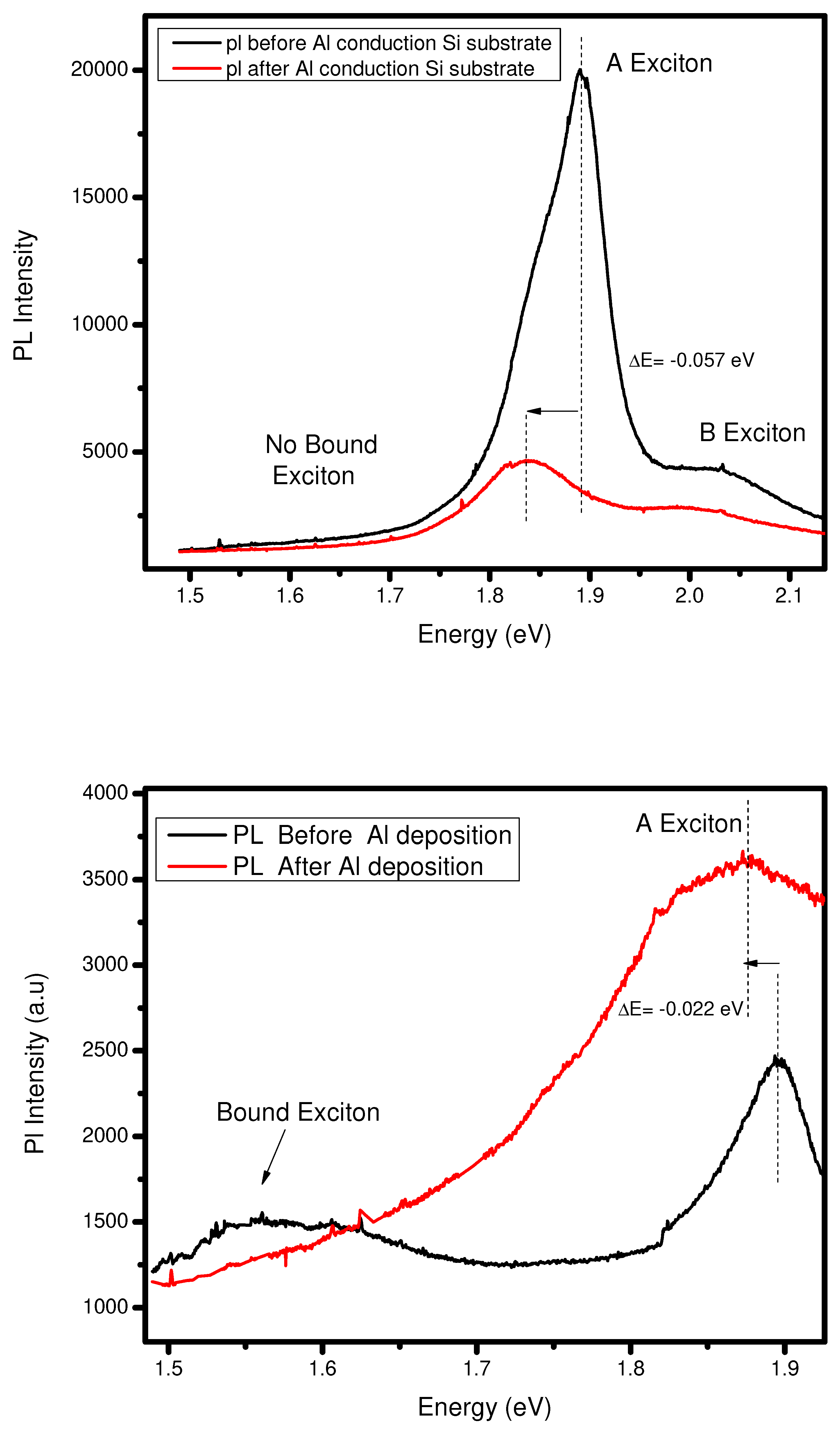
Figure 11.
(a) Raman before and after PVD of 1nm Al on bilayer and Silicon as substrate .(b) Raman before and after PVD of 1nm Al on bilayer and PDMS as substrate .
Figure 11.
(a) Raman before and after PVD of 1nm Al on bilayer and Silicon as substrate .(b) Raman before and after PVD of 1nm Al on bilayer and PDMS as substrate .
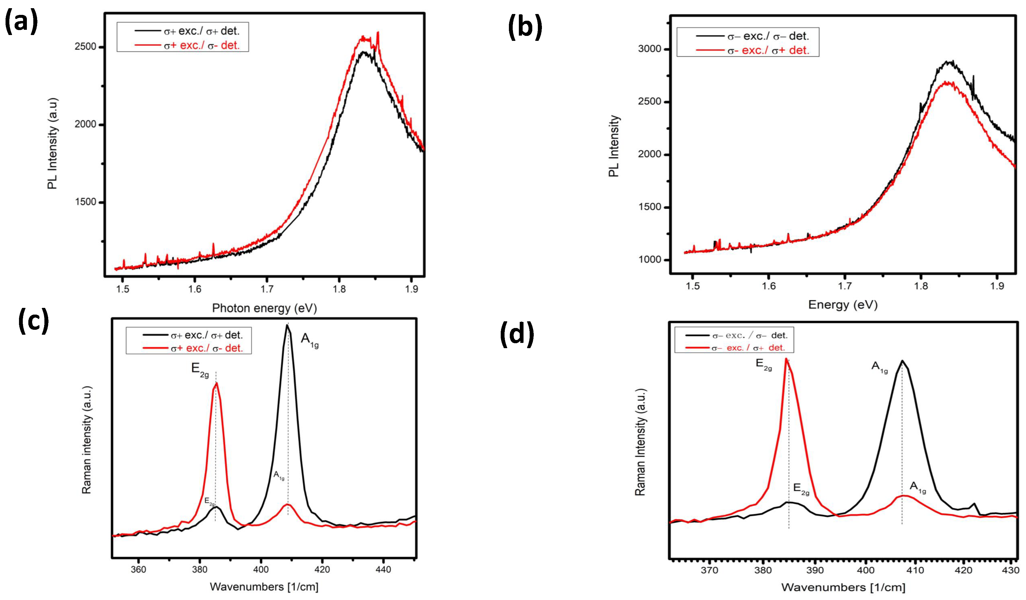
Helicity-resolved photoluminescence and Raman study of monolayer and
In helicity-resolved spectra, with the circularly polarization light, we observed the helicity of photons emission for co-polarization (co-valley) and cross-polarization (opposite valley) and the same for the helicity measurement of photons emission after the phonons inelastically scatter them. So, we measure that the excitation by specific helicity results in the selective helicity emission of photons to co-valley or cross valley in PL case and the helicity selective scattering of Raman vibrational modes for Raman case. First, in helicity for monolayer , we observed the excitation with the application of right circularly polarized light ( +), and detection is shown for both + (co-polarization) and - (cross-polarization) see Figure 12 (a). we observe the same PL intensity and peak as the emission is the same in co and cross valley. For the Raman case, we observe the selective helicity scattering of and modes (see Figure 12(b)).
Now, if we look into the 1nm Al deposition on bilayer , and we selectively make excitation with the application of right circularly polarization light ( +) and detection as we observed above, see Figure 13 (a), the photons detection from cross-polarization ( -) is more than the co polarization. In the Raman case, if we make selective excitation by + and detect the selective scattering of and for co and cross-polarization. See Figure 13 (c). We observed the mode and measured the scattering of vibrational mode with very low intensity when we have + detection—the same case for the - detection in vice versa scattering of vibrational modes. The low-intensity vibrational modes start to appear due to softening of the helicity selection rule. This proves that Al deposition on flake made some changing in the scattering phenomenon of Raman modes.
References
- Losurdo, Maria, CNR NANOTEC, and Kurt Hingerl. "Twinning for Improving Capacity of Research in Multifunctional Nanosystems for Optronic Biosensing.
- (Ong Kim Le, Viorel Chihaia, My-Phuong Pham-Ho and Do Ngoc Son Electronic and optical properties of monolayer MoS2 under the influence of polyethyleneimine adsorption and pressure[2020]).
- Byun, Kyung-Eun, Hyun-Jong Chung, Jaeho Lee, Heejun Yang, Hyun Jae Song, Jinseong Heo, David H. Seo et al. "Graphene for true ohmic contact at metal–semiconductor junctions." Nano letters 13, no. 9 (2013): 4001-4005. [CrossRef]
- Rao, C. N. R., K. Gopalakrishnan, and Urmimala Maitra. "Comparative study of potential applications of graphene, MoS2, and other two-dimensional materials in energy devices, sensors, and related areas." ACS applied materials interfaces 7, no. 15 (2015): 7809-7832. [CrossRef]
- Ahuja, Ushma, Alpa Dashora, Harpal Tiwari, Dushyant C. Kothari, and K. Venugopalan. "Electronic and optical properties of MoS2–WS2 multi-layers: First principles study." Computational materials science 92 (2014): 451-456. [CrossRef]
- Molina-Sanchez, A., Hummer, K., Wirtz, L. (2015). Vibrational and optical properties of MoS2: From monolayer to bulk. Surface Science Reports, 70(4), 554-586. [CrossRef]
- Ong Kim Le, Viorel Chihaia, My-Phuong Pham-Ho and Do Ngoc Son Electronic and optical properties of monolayer MoS2 under the influence of polyethyleneimine adsorption and pressure[2020].
- Wang, Q., Shao, Y., Shi, X. (2020). Mechanism of charge redistribution at the metal–semiconductor and semiconductor–semiconductor interfaces of metal–bilayer MoS2 junctions. The Journal of Chemical Physics, 152(24). [CrossRef]
- Xu, Y., Cheng, C., Du, S., Yang, J., Yu, B., Luo, J., ... Duan, X. (2016). Contacts between two-and three-dimensional materials: Ohmic, Schottky, and p–n heterojunctions. ACS nano, 10(5), 4895-4919. [CrossRef]
- Liu, Y., Guo, J., Zhu, E., Liao, L., Lee, S. J., Ding, M., ... Duan, X. (2018). Approaching the Schottky–Mott limit in van der Waals metal–semiconductor junctions. Nature, 557(7707), 696-700. [CrossRef]
- S. S. Dhanabalan, A. Thirumurugan, G. Periyasamy “Surface engineering of high-temperature PDMS substrate for flexible optoelectronic applications” Volume 800, August 2022, 139692. [CrossRef]
- Just, Th. (April 1938). "G. W. Steller". Die Naturwissenschaften. 26 (14): 224. Bibcode:1938NW.....26..224J. [CrossRef]
- SooHo Choi, Zhang Shaolin and Woochul Yang, Department of Physics, Dongguk University, Seoul 100-715, Korea,2014 “Layer-number-dependent Work Function of MoS2 Nanoflakes”.
- Hyung-Jun Kim, Suk Yang, Hojoong Kim, Jin Young Moon , Kyung Park , Yun-Jin Park, and Jang-Yeon Kwon, Nano Research 2018.
- Kim, H. J., Yang, S., Kim, H., Moon, J. Y., Park, K., Park, Y. J., Kwon, J. Y. (2018). Enhanced electrical and optical properties of single-layered MoS 2 by incorporation of aluminum. Nano Research, 11, 731-740. [CrossRef]
- Merida, C. S., Le, D., Echeverria, E. M., Nguyen, A. E., Rawal, T. B., Naghibi Alvillar, S., ... Bartels, L. (2018). Gold dispersion and activation on the basal plane of single-layer MoS2. The Journal of Physical Chemistry C, 122(1), 267-273. [CrossRef]
Figure 3.
shows the process of transferring of flakes on substrate.
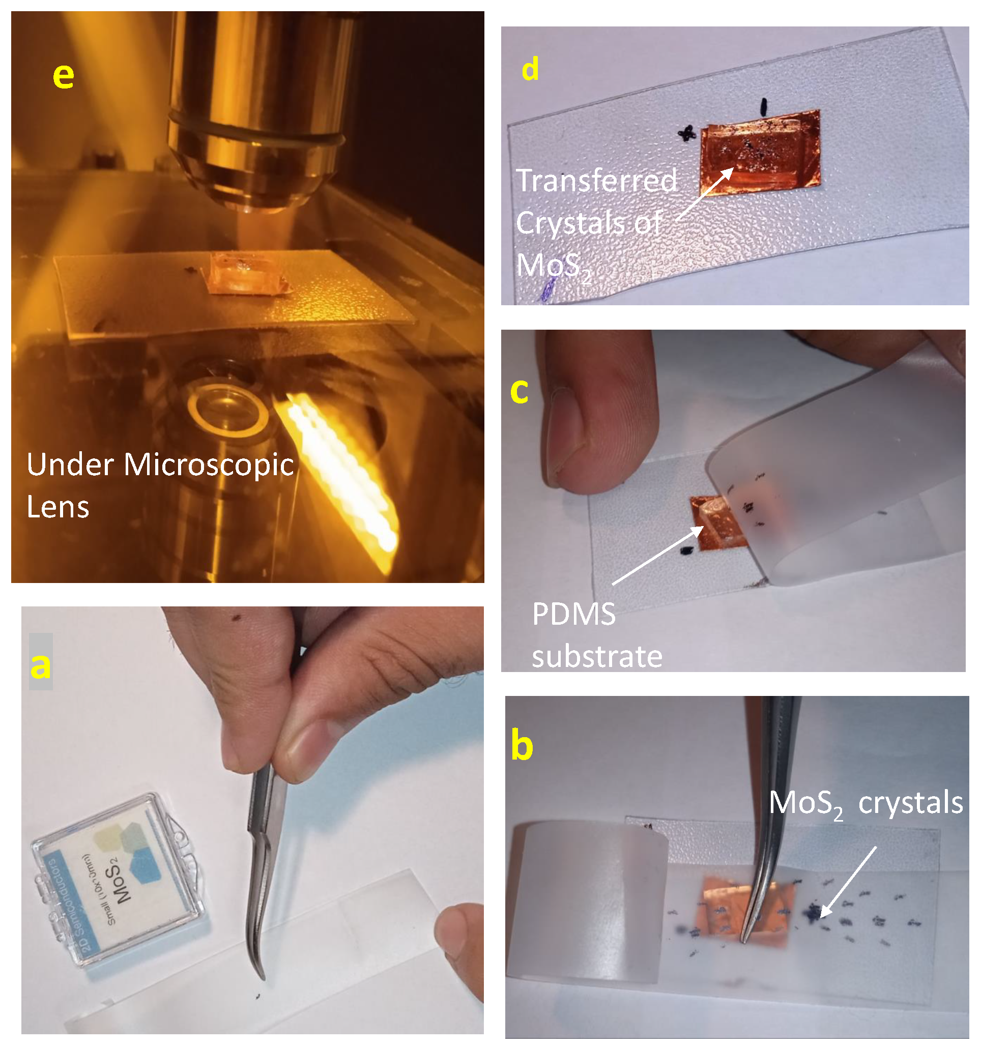
Figure 9.
(a) Raman before and after megnetron sputtering of 5nm gold on bilayer and PMDS as substrate .(b) Raman before and after PVD of 1nm Al on bilayer and PDMS as substrate.
Figure 9.
(a) Raman before and after megnetron sputtering of 5nm gold on bilayer and PMDS as substrate .(b) Raman before and after PVD of 1nm Al on bilayer and PDMS as substrate.
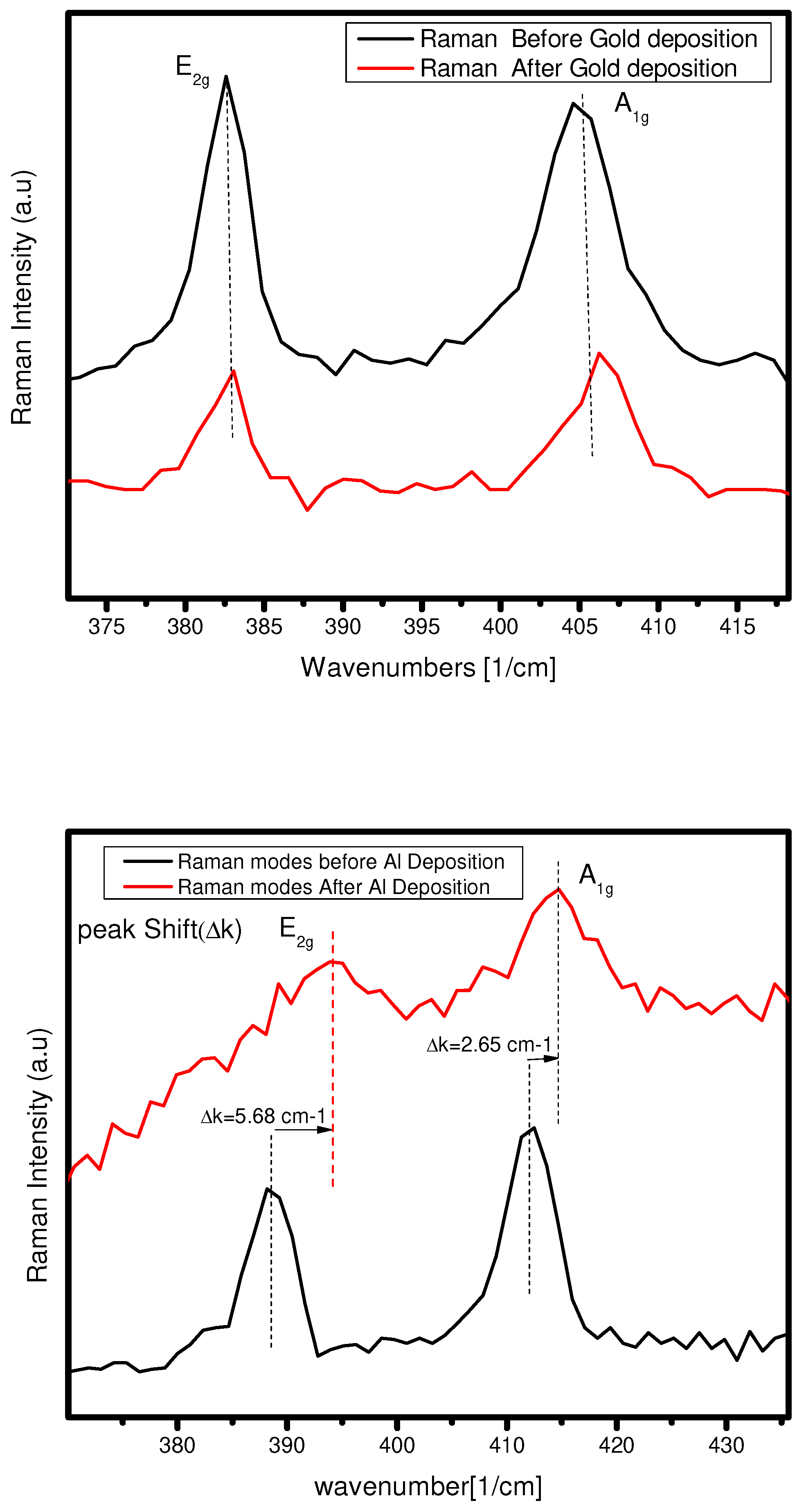
Figure 12.
(a)Photoluminescence helicity of (b) Raman helicity of .
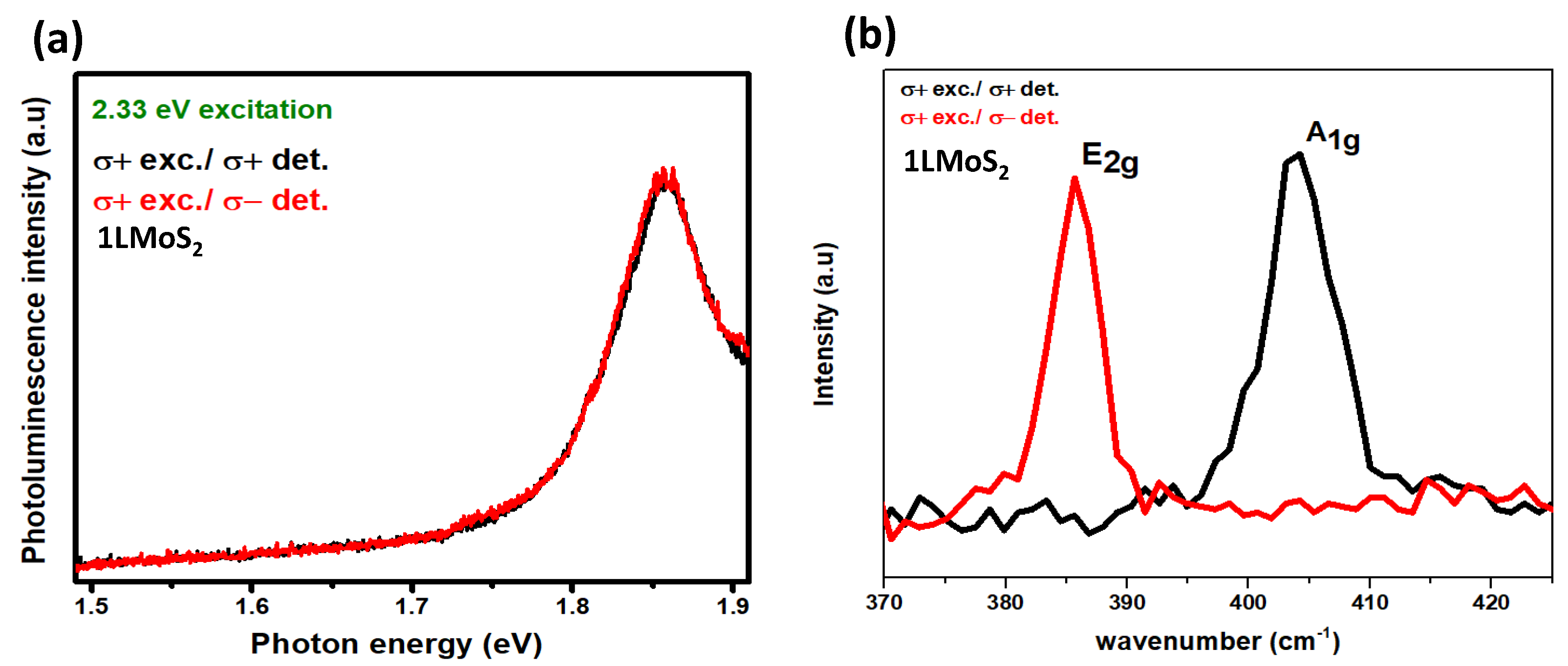
Figure 13.
(a)Photoluminescence helicity of with the excitation of +. (b) Photoluminescence helicity of . (c) Raman helicity of with + excitation.(d) Raman helicity of with - excitation.
Figure 13.
(a)Photoluminescence helicity of with the excitation of +. (b) Photoluminescence helicity of . (c) Raman helicity of with + excitation.(d) Raman helicity of with - excitation.
Disclaimer/Publisher’s Note: The statements, opinions and data contained in all publications are solely those of the individual author(s) and contributor(s) and not of MDPI and/or the editor(s). MDPI and/or the editor(s) disclaim responsibility for any injury to people or property resulting from any ideas, methods, instructions or products referred to in the content. |
© 2023 by the authors. Licensee MDPI, Basel, Switzerland. This article is an open access article distributed under the terms and conditions of the Creative Commons Attribution (CC BY) license (http://creativecommons.org/licenses/by/4.0/).
Copyright: This open access article is published under a Creative Commons CC BY 4.0 license, which permit the free download, distribution, and reuse, provided that the author and preprint are cited in any reuse.


