1. Introduction
The issues of environmental pollution and energy crisis are escalating at an alarming rate. Currently, in the conventional procedure of utilizing fossil energy, only a relatively minor portion of the mineral energy is transformed and employed, with the majority of the remaining energy being dissipated as heat [
1]. Extensive studies have been conducted by scientists to discover renewable and eco−friendly energy sources while enhancing energy efficiency. Carrier and phonon transmission characteristics within solid materials are utilized by thermoelectric materials to achieve the direct conversion between electric energy and heat energy, emerging as a novel environmentally−friendly energy material [
2]. The dimensionless optimal values determine the thermoelectric characteristics of materials, which can be obtained using the equation by ZT = S
2σT/κ. Here, S, σ, T, and κ represent the Seebeck coefficient, electrical conductivity, absolute temperature, and thermal conductivity, respectively [
3,
4,
5]. Nonetheless, the interdependence of S, ρ, and κ poses a barrier to the collaborative enhancement of thermoelectric performance, presenting a significant obstacle in achieving simultaneous optimization of multiple parameters [
6,
7]. The concept of phonon glass electron crystals offers a potential solution to this puzzle [
8]. The low thermal conductivity and high Seebeck coefficient of the BiCuSeO system have garnered significant interest [
9,
10,11].
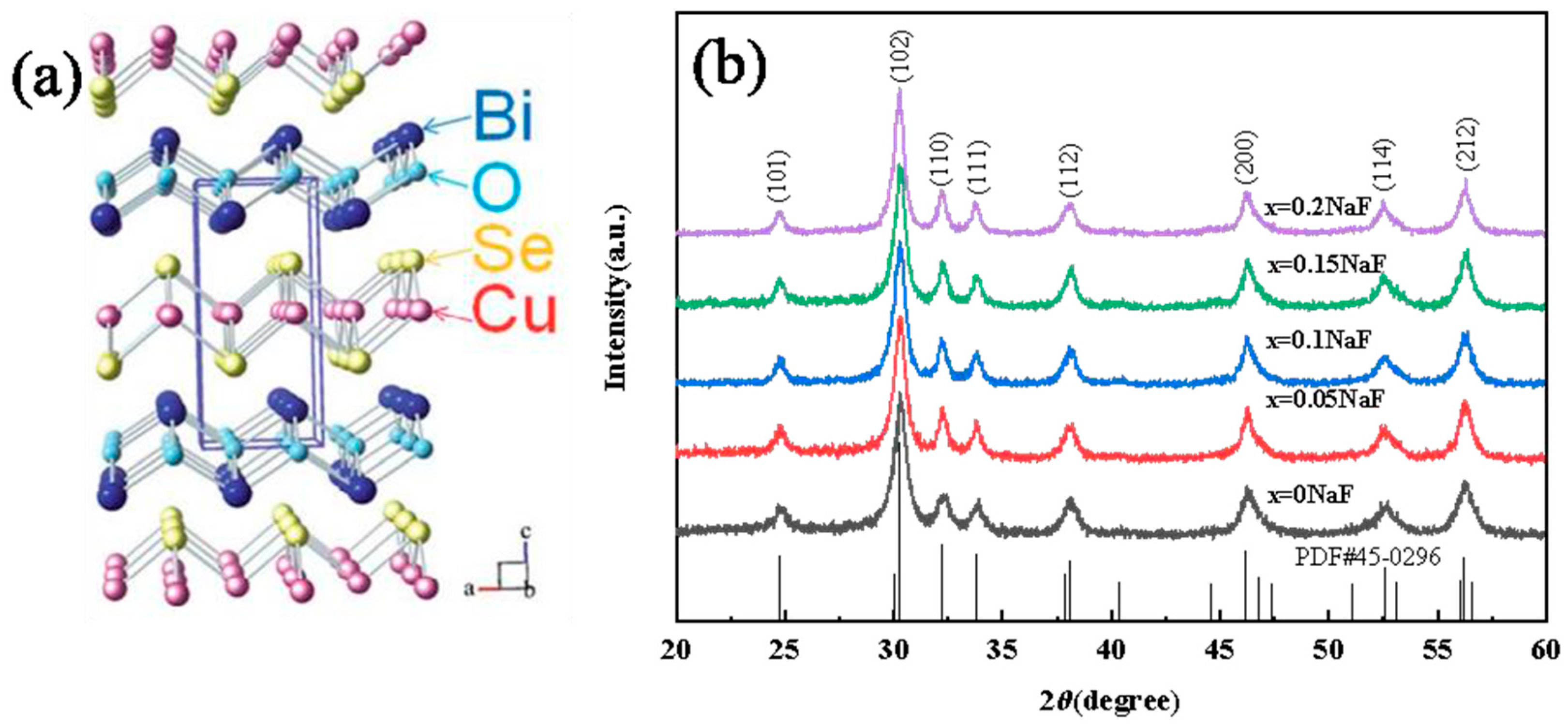
Figure 1a illustrates that BiCuSeO has a layered structure of the ZrCuSiAs type and is classified under the P4/nmm space group. The crystal structure consists of a stack of alternating layers along the C−axis direction. These layers include an insulating layer (Bi
2O
2)
2+ and a conducting layer (Cu
2Se
2)
2−. The Bi
2O
2 layer serves as a charge storage layer, composed of a slightly deformed Bi
4O octahedron with shared Bi−Bi edges. On the other hand, the Cu
2Se
2 layer acts as a transport surface for carrier transport, composed of slightly deformed CuSe
4 tetrahedra with shared Se−Se sides [12−14]. Furthermore, the feeble chemical linkage amidst the two layers and the junction connecting them enhance phonon scattering, leading to an extremely low thermal conductivity (0.40 Wm
−1K
−1 at 923 K) [
9].
Nonetheless, BiCuSeO exhibits a significantly limited conductivity as a result of its low hole concentration, thereby impeding the attainment of a high ZT value. In order to enhance the conductivity of BiCuSeO, the researchers enhanced the material's conductivity through element doping, optimized the carrier concentration by adjusting the band gap, and increased the carrier mobility through texturization [18,19]. Doping monovalent elements (Na+, K+, Ag+, etc.) or bivalent elements (Mg2+, Ca2+, Ba2+, Pb2+, etc.) at the Bi site or by increasing the concentration of hole carriers through Bi, Cu, O vacancies and ball−milling is used to improve the thermoelectric performance of BiCuSeO [10−13,15−17]. Furthermore, the technique of dual doping is another efficient approach for enhancing the thermoelectric performance of materials. Sun et al enhanced the thermoelectric characteristics of BiCuSeO by introducing Zn into the Bi position and S into the O position, resulting in a ZT value of 0.68 at 750 K [20]. Kuang−kun Ren et al introduced dopants of Pb and Te into the Bi and Se positions, respectively. The substitution of Te at Se sites significantly decreased the extent of chemical bonding and the mass of effective carriers. Consequently, this weakened the coupling between carriers and phonons, enhancing carrier mobility and resulting in high conductivity [21]. By employing mechanical alloying, the BiCuSeO system achieved a ZT value of 1.08 through the introduction of Pb and Ni elements into the Bi and Cu sites [18]. The replacement of Bi elements with Pb and In elements resulted in the ZT value of the BiCuSeO system reaching 1.23 [22]. Liu et al. reported that the addition of Pb and Ca elements into the Bi site of BiCuSeO not only improved the conductivity and thermal conductivity, but also enhanced the effective mass of carriers, thereby maintaining a high Seebeck coefficient for the material. Consequently, the doped BiCuSeO achieved a ZT value of 1.5 [23], which stands as the highest value within the present system.
The above results show that co−doping of elements can enhance the thermoelectric performance of BiCuSeO. Although there have been numerous reports on the Bi, Cu, and Se dopants of BiCuSeO, there is comparatively less information available on the O−dopants. Furthermore, studies [
10] and [24] have indicated that the thermoelectric performance of the BiCuSeO system can be enhanced through O−site doping of F and S elements. The majority of the materials are synthesized through the sintering technique of solid state reaction. The drawback of this approach is the lengthy requirement for calcination of the raw materials, whereas the high−energy ball milling technique enables rapid synthesis of the raw materials. Considering this, the rapid synthesis of Na and F co−doped BiCuSeO ceramic samples was achieved using the high energy ball milling technique. A systematic study was conducted on the impact of combining sodium in the bismuth position and fluorine in the oxygen position on the microstructure and thermoelectric performance of BiCuSeO.
3. Results and Discussion
The XRD patterns of Bi
1−xNa
xCuSeO
1−xF
x(x=0, 0.05, 0.10, 0.15, and 0.20) ceramics is depicted in
Figure 1b. Compared to the standard card of BiCuSeO (PDF#45−0296), the diffraction peak position of the Bi
1−xNa
xCuSeO
1−xF
x was consistent with that of the standard card. The results show that the synthesized Bi
1−xNa
xCuSeO
1−xF
x ceramics is a single phase. As the NaF doping amount increased, the XRD peak of Bi
1−xNa
xCuSeO
1−xF
x ceramics experienced a slight rightward shift. This shift occurred due to the slightly smaller ionic radius of Na
+ (0.102 nm) compared to Bi
3+ (0.103 nm), and the smaller ionic radius of F
−(0.133 nm) compared to O
2− (0.140 nm). This makes the crystal plane spacing smaller. The crystal face spacing and the lattice constants are were calculated using the Bragg Eqs. (1) and (2):
where d, a, and c represents the crystal plane spacing, and lattice parameters, correspondingly.
Table 1 displays the lattice constants a and c of Bi
1−xNa
xCuSeO
1−xF
x (x=0, 0.05, 0.10, 0.15, and 0.20) ceramics. The crystal face spacing of Bi
1−xNa
xCuSeO
1−xF
x ceramic sample was calculated by the equation (2), and it was found that the change of crystal face spacing was very small. Therefore, the diffraction peak of Bi
1−xNa
xCuSeO
1−xF
x ceramics did not appear obvious deviation.
Table 1 shows the calculation of the grain size for Bi
1−xNa
xCuSeO
1−xF
x ceramics using the Debye−Scherrer formula Dc = 0.89λ/(Bcosθ), where B represents the half−peak width and θ signifies the Bragg diffraction Angle. The results show that the average grain sizes of Bi
1−xNa
xCuSeO
1−xF
x(x=0, 0.05, 0.10, 0.15, and 0.20) ceramics are 1.92 μm, 1.63 μm, 1.66 μm, 1.68 μm, and 1.72 μm, correspondingly. Following the addition of NaF, the average grain size of the Bi
1−xNa
xCuSeO
1−xF
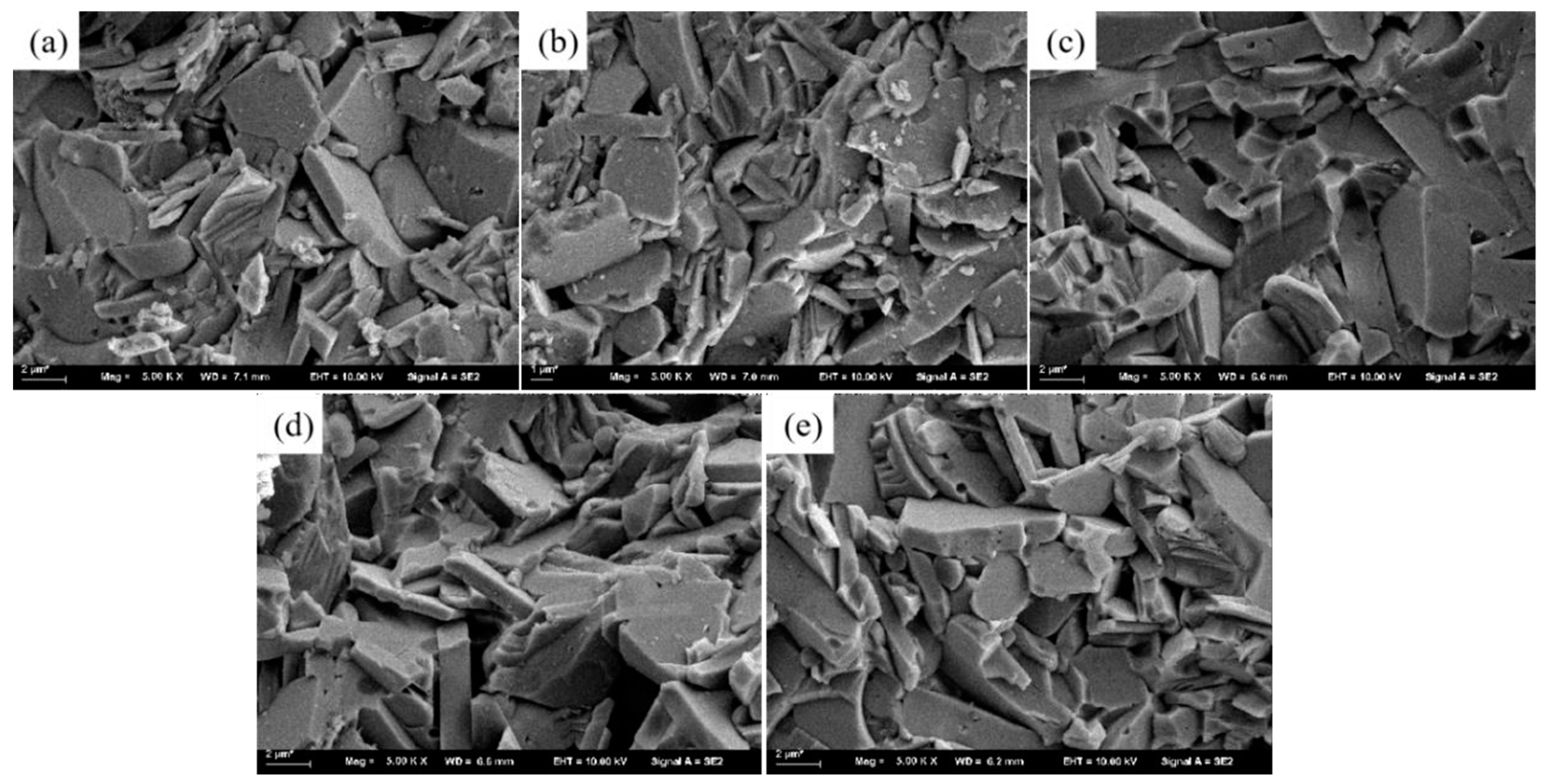
x samples is marginally reduced compared to the pure BiCuSeO sample. The fracture morphology of Bi
1−xNa
xCuSeO
1−xF
x(x=0, 0.05, 0.10, 0.15, and 0.20) ceramics is shown in
Figure 2, illustrating the layered structures. According to
Figure 2, the average grain size of Bi
1−xNa
xCuSeO
1−xF
x samples exhibited a pattern of initial decrease and subsequent increase as the NaF doping amount increased, aligning with the results obtained from the Scherrer formula calculations.
XPS determination was conducted on the Bi
1−xNa
xCuSeO
1−xF
x (x = 0,0.05, 0.10, 0.15, and 0.20) ceramics to ascertain the valence states of each element.
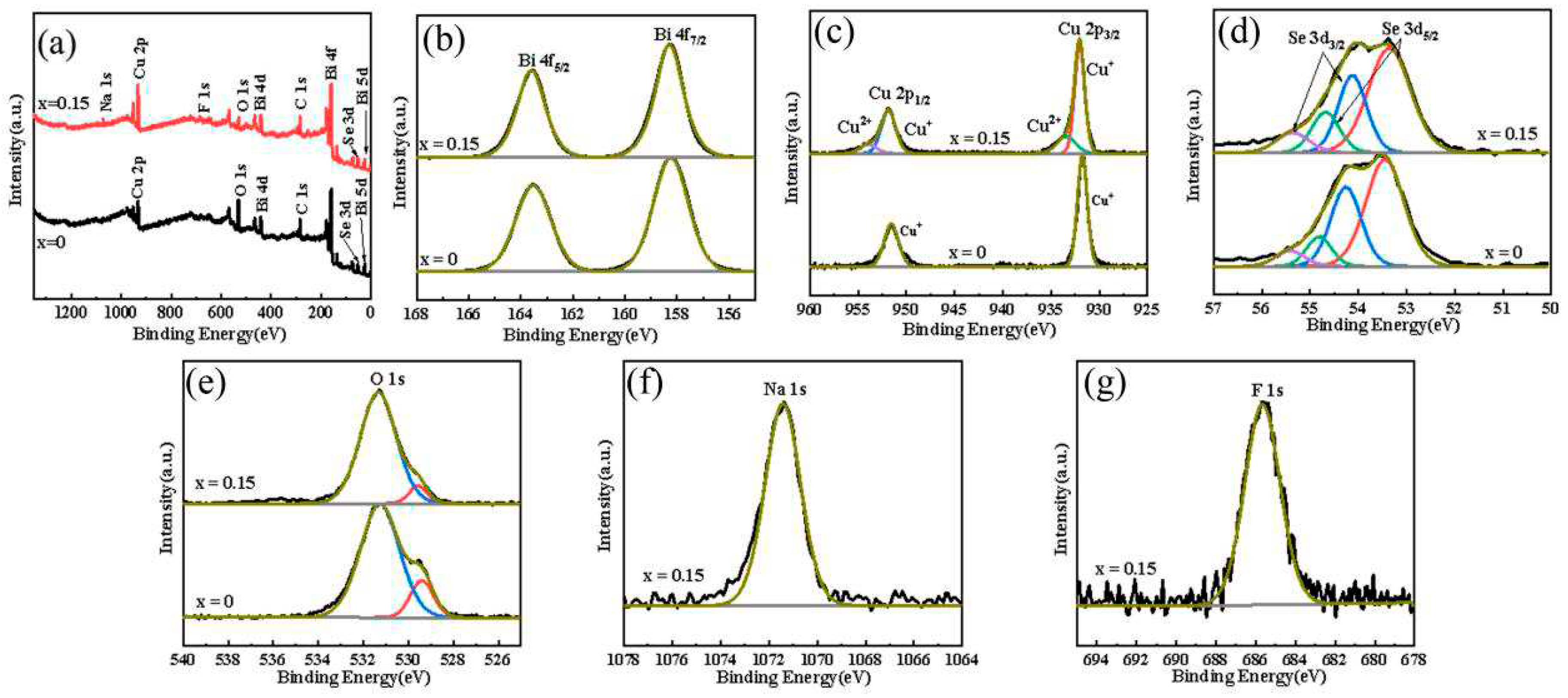
Figure 3a shows the full spectrum of XPS of Bi
1−xNa
xCuSeO
1−xF
x (x=0, 0.15) ceramic sample. It can be seen from the full spectrum that the undoped sample contains Bi, Cu, Se and O elements, while the doped NaF sample contains Bi, Cu, Se, O, Na and F elements. Combined with XRD results, it is possible to verify the successful integration of Na and F elements into the BiCuSeO system. The XPS high−resolution spectra of Bismuth (Bi), Copper (Cu), Selenium (Se), Oxygen (O), and Sodium (Na) in the samples of Bi
1−xNa
xCuSeO
1−xF
x (x=0, 0.15) samples are displayed in Fgure 3(a)−(f). The high−resolution spectra of Bi 4f in
Figure 3b exhibits two spin−orbit peaks, which correspond to the spin−orbit peak of Bi 4f
7/2 and the spin−orbit peak of Bi 4f
5/2, respectively. The two distinctive peaks can be found at 158.28 eV and 163.58 eV correspondingly, with a disparity of 5.3 eV, suggesting the presence of Bi atoms in the Bi
3+ state [17,25,26]. As shown in the
Figure 3c, the 2p orbits of Cu elements in the pure BiCuSeO sample split into two distinct peaks, namely the spin−orbit peak of Cu 2p
3/2 at 931.68 eV and the spin−orbit peak of Cu 2p
1/2 at 951.58 eV. These peaks exhibit a difference of 19.9 eV, indicating the presence of Cu+ ions in the sample. The spin−orbit splitting of Cu 2p in the Bi
0.85Na
0.15CuSeO
0.85F
0.15 sample is divided into four peaks. According to the results, Cu
2+ is observed in the Bi
0.85Na
0.15CuSeO
0.85F
0.15, which aligns with the outcomes documented in the literature [26].
Figure 3d shows the Se 3d high−resolution spectrum. The spin−orbit splitting is quite intricate, with the spin−orbit peaks of Se 3d
5/2 located at 53.48 eV and 54.88 eV, respectively. The spin−orbit peaks of Se 3d
3/2 were found at 54.28 eV and 55.48 eV, correspondingly. The presence of Se atoms in the form of Se
2− is indicated by the low binding energy of the Se 3d
5/2 and Se 3d
3/2 spin−orbit peaks, while the interaction between the layers of Se is indicated by the high binding energy of the spin−orbit peaks, which aligns with the results documented in the literature [26]. The high−resolution spectrum of O 1s in
Figure 3e reveals two spin−orbit peaks. The peak at 529.4 eV represents lattice oxygen, whereas the high binding energy peak signifies oxygen vacancy. To ascertain the alteration in oxygen content for the two types, the ratio of the two peaks' areas was employed. The area ratio of lattice oxygen to oxygen vacancy in the BiCuSeO sample is 0.2, while the area ratio of lattice oxygen to oxygen vacancy in the Bi
0.85Na
0.15CuSeO
0.85F
0.15 sample is 0.09. The results indicate that the doping of NaF increases the lattice defect in Bi
1−xNa
xCuSeO
1−xF
x sample, which aligns with the results reported documented in the literature [27,28].
Figure 3f shows the high−resolution spectrum of Na 1s in Bi
0.85Na
0.15CuSeO
0.85F
0.15 samples. The Na 1s orbital exhibits a solitary peak, indicating that Na exists with a +1 valence, which aligns with the results documented in the literature [29]. The 1s spin-orbit peak of F in
Figure 3g, indicates the presence of F
− in a manner consistent with the results reported in the literature[30].
The temperature−dependent electrical conductivity (σ) of the Bi
1−xNa
xCuSeO
1−xF
x (x = 0, 0.05, 0.10, 0.15, and 0.20
) ceramics is shown in
Figure 4a. For the pure BiCuSeO sample, the conductivity is very low throughout the test temperature range, and is significantly improved after doping. The σ of Bi
1−xNa
xCuSeO
1−xF
x ceramics increases as the NaF doping increases in the whole temperature range. At 323 K, the conductivity increases from 9.10 S cm
−1 (BiCuSeO) to 94.50 S cm
−1 (Bi
0.80Na
0.20CuSeO
0.80F
0.20), resulting in a significant increase of 900%. The rise in the carrier concentration of the system is the primary cause for the enhanced conductivity of Bi
1−xNa
xCuSeO
1−xF
x (x = 0, 0.05, 0.10, 0.15, and 0.20) ceramics. The relationship between conductivity σ and carrier concentration and mobility can be expressed as
σ=
enu, where
e represents the electron charge,
n denotes the carrier concentration, and
μ represents the carrier mobility. The carrier concentration is determined using the expression
n=1/
eRH.
Table 2 demonstrates the carrier concentration and mobility of Bi
1−xNa
xCuSeO
1−xF
x (x = 0, 0.05, 0.10, 0.15, and 0.20) ceramics. Upon the addition of NaF, the electrical conductivity σ initially declines and subsequently rises as the testing temperature increases, reaching an inflection point at 523 K. Within the temperature range from 323 K to 523 K, the conductivity of the doped ceramics diminishes with rising temperature, exhibiting degenerate semiconductor characteristics. As the temperature exceeds 523 K, the sample's conductivity rises in proportion to the temperature increase. The sample displays semiconductor performance that are not degenerate due to its intrinsic excitation. The conductivity of Bi
0.80Na
0.20CuSeO
0.80F
0.20 reaches a maximum of 108.6 S cm
−1 at 823 K.
Figure 4b shows temperature−dependent S of Bi
1−xNa
xCuSeO
1−xF
x (x=0, 0.05, 0.10, 0.15, and 0.20) ceramics. The signs for all Seebeck coefficients are positive, indicating that the Bi
1−xNa
xCuSeO
1−xF
x ceramic functions as a P-type semiconductor with predominantly hole charge carriers. The Seebeck coefficient of BiCuSeO exhibits a value of 349 uV K
−1 at 323 K, while it shows a value of 324 uV K
−1 at 823 K.The Seebeck coefficient of Bi
1−xNa
xCuSeO
1−xF
x samples decreases as NaF doping content increases at 300 K. In the case of degenerate semiconductors, if we assume a parabolic band structure and use the phonon scattering approximation, the Pisarenko relationship can provide a rough representation of S [31,32].
The Seebeck coefficient (
S), Boltzmann constant (
kB), absolute temperature (
T), carrier charge (
e), reduced Planck constant (
h), carrier effective mass (
m*), and carrier concentration (
n) are all related in this equation. Formula (3) reveals that the Seebeck coefficient varies inversely with the carrier concentration and directly with the effective mass. The effective mass m* is calculated by formula (3), as shown in
Table 2. The effective mass m* increases as the NaF doping content increases, going from 2.094 m
0 in the pure sample to 6.5043 m
0 in the Bi
0.85Na
0.15CuSeO
0.85F
0.15 sample. The results indicate that the decline in Seebeck coefficient of Bi
1−xNa
xCuSeO
1−xF
x ceramics primarily arises from the rise in increase of carrier concentration within the system.
The power factor of Bi
1−xNa
xCuSeO
1−xF
x (x = 0, 0.05, 0.10, 0.15, and 0.20) ceramics is determined by the formula
PF=
S2σ. The temperature dependent curves for the power factor are shown in
Figure 4c. The PF of all doped samples is higher than that of pure BiCuSeO throughout the entire temperature range due to a substantial conductivity increase. At room temperature, the Bi
0.90Na
0.10CuSeO
0.90F
0.10 samples have the highest power factor, reaching 16.7 × 10
−5 W/m K
−2. As the temperature increases, the power factor of Bi
0.85Na
0.15CuSeO
0.85F
0.15 samples gradually surpasses that of Bi
0.90Na
0.10CuSeO
0.90F
0.10 samples. At 823 K, the Bi
0.85Na
0.15CuSeO
0.85F
0.15 sample exhibits a maximum power factor of 44.8 × 10
−5 W/m K
2, which is approximately 7.11 times higher than that of the pure BiCuSeO sample (6.3×10
−5 W/mK
2).
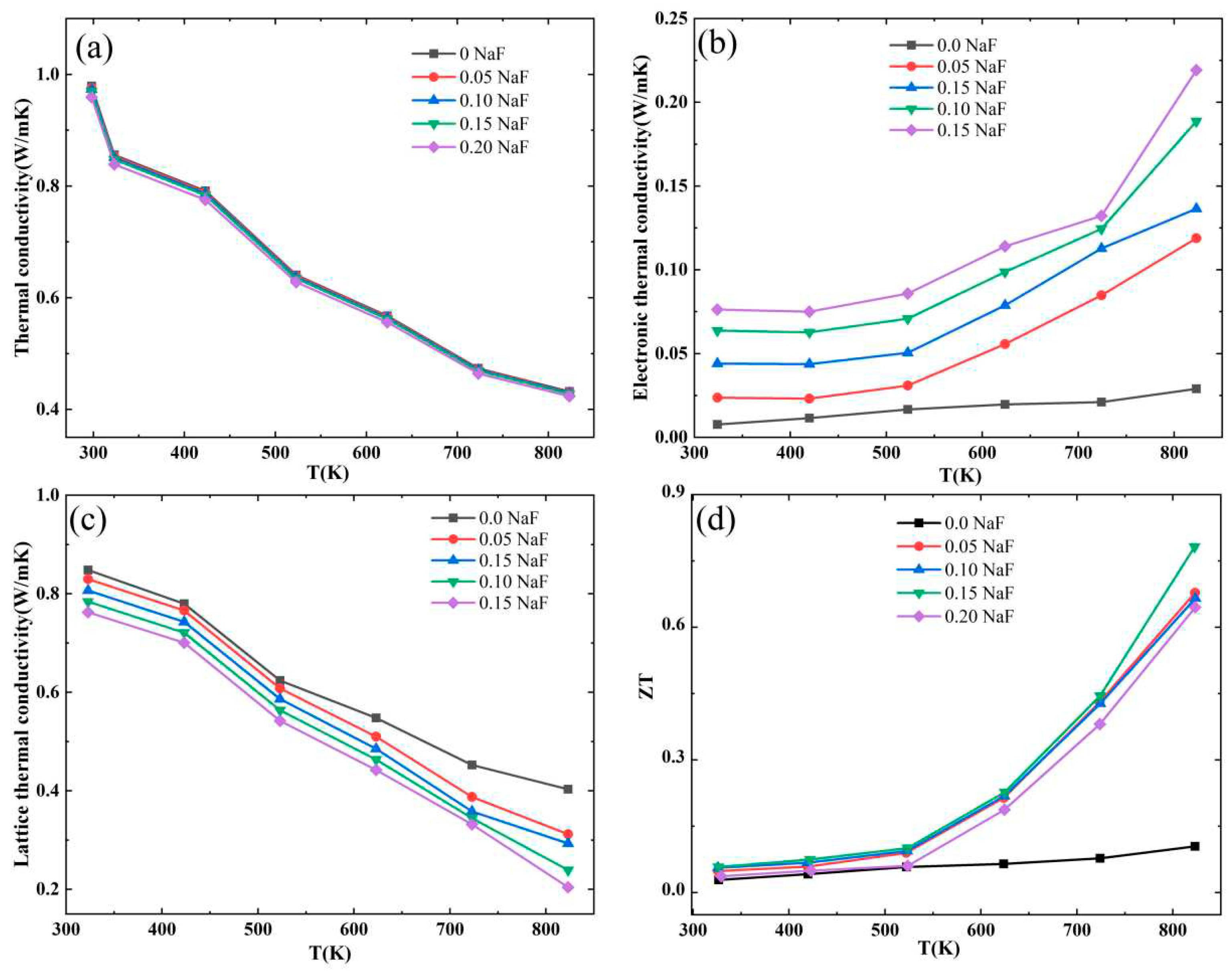
Figure 5a shows thermal conductivity (κ) as a function of temperature for Bi
1−xNa
xCuSeO
1−xF
x (x = 0, 0.05, 0.10, 0.15, and 0.20) ceramics. The thermal conductivity κ of BiCuSeO significatly decreases from 0.98 Wm
−1 K
−1 at 323 K to 0.43 Wm
−1 K
−1 at 823 K, while the thermal conductivity remained virtually unchanged even after the introduction of NaF doping. Typically, the total thermal conductivity consists of the electron thermal conductivity κ
e and the lattice thermal conductivity κ
l. The electron thermal conductivity is usually calculated by Wiedemane−Franz relationship (
) , where σ is the electrical conductivity, T is the absolute temperature, and L is the Lorentz constant which can be calculated by the formula
. Lorentz constant L is calculated using Sommerfeld value L
0= 2.44×10
−8 W Ω K
−2.
Figure 5b displays the temperature dependence of the electron thermal conductance κ
e of Bi
1−xNa
xCuSeO
1−xF
x (x = 0, 0.05, 0.10, 0.15, and 0.20) ceramics. The figure illustrates that the electron thermal conductivity of Bi
1−xNa
xCuSeO
1−xF
x ceramics exhibits a rising pattern as the doping level increases. The primary reason for this is primarily the rise in electrical conductance. At 823 K, the maximum electron thermal conductivity of Bi
0.8Na
0.2CuSeO
0.8F
0.2 ceramics reaches 0.219 W m
−1 K
−1. The results indicate that the lattice thermal conductivity is dominant in the BiCuSeO system.
The temperature-dependent lattice thermal conductivity of Bi
1−xNa
xCuSeO
1−xF
x (x = 0, 0.05, 0.10, 0.15, and 0.20) ceramics is illustrated in
Figure 5c. The lattice thermal conductivity of Bi
1−xNa
xCuSeO
1−xF
x samples declines as the temperature rises. This was primarily due to the intensification of lattice vibration and the enhanced scattering ability of phonons, resulting in a decrease in lattice thermal conductivity as temperature increases. Compared to the pure BiCuSeO sample, the lattice thermal conductivity of Bi
1−xNa
xCuSeO
1−xF
x ceramics decreases, primarily due to the reduction in grain size caused by NaF doping.
Table 1 displays that the grain sizes of Bi
1−xNa
xCuSeO
1−xF
x (x = 0, 0.05, 0.10, 0.15, and 0.20) ceramics are 1.92 μm, 1.63 μm, 1.66 μm, 1.68 μm, and 1.72 μm, respectively. The grain sizes of the doped samples are smaller compared to the pure BiCuSeO sample, leading to an improved ability for scattering phonons. Hence, the lattice thermal conductivity of Bi
1−xNa
xCuSeO
1−xF
x ceramics doped with NaF decreases as the doping amount increases.
The ZT as a function of temperature for Bi1−xNaxCuSeO1−xFx (x = 0, 0.05, 0.10, 0.15, and 0.20) ceramics is illustrated in figure 5(d). The ZT value of Bi1−xNaxCuSeO1−xFx samples is primarily determined by its electrical conductivity due to the insignificant variation in thermal conductivity.The figure illustrates that the ZT value of all samples exhibits an increasing trend with the increase of test temperature. At 823 K, and Bi0.85Na0.15CuSeO0.85F0.15 achieves a peak value of 0.78, which is 7.09 times greater than that of pure BiCuSeO. The results indicate that the addition of NaF can greatly enhance the thermoelectric performance of BiCuSeO.


