Submitted:
19 November 2023
Posted:
21 November 2023
You are already at the latest version
Abstract
Keywords:
1. Introduction
2. Modeling of cross-coupled CMOS AC – DC charge pump (XC – CP) operating in subthreshold region
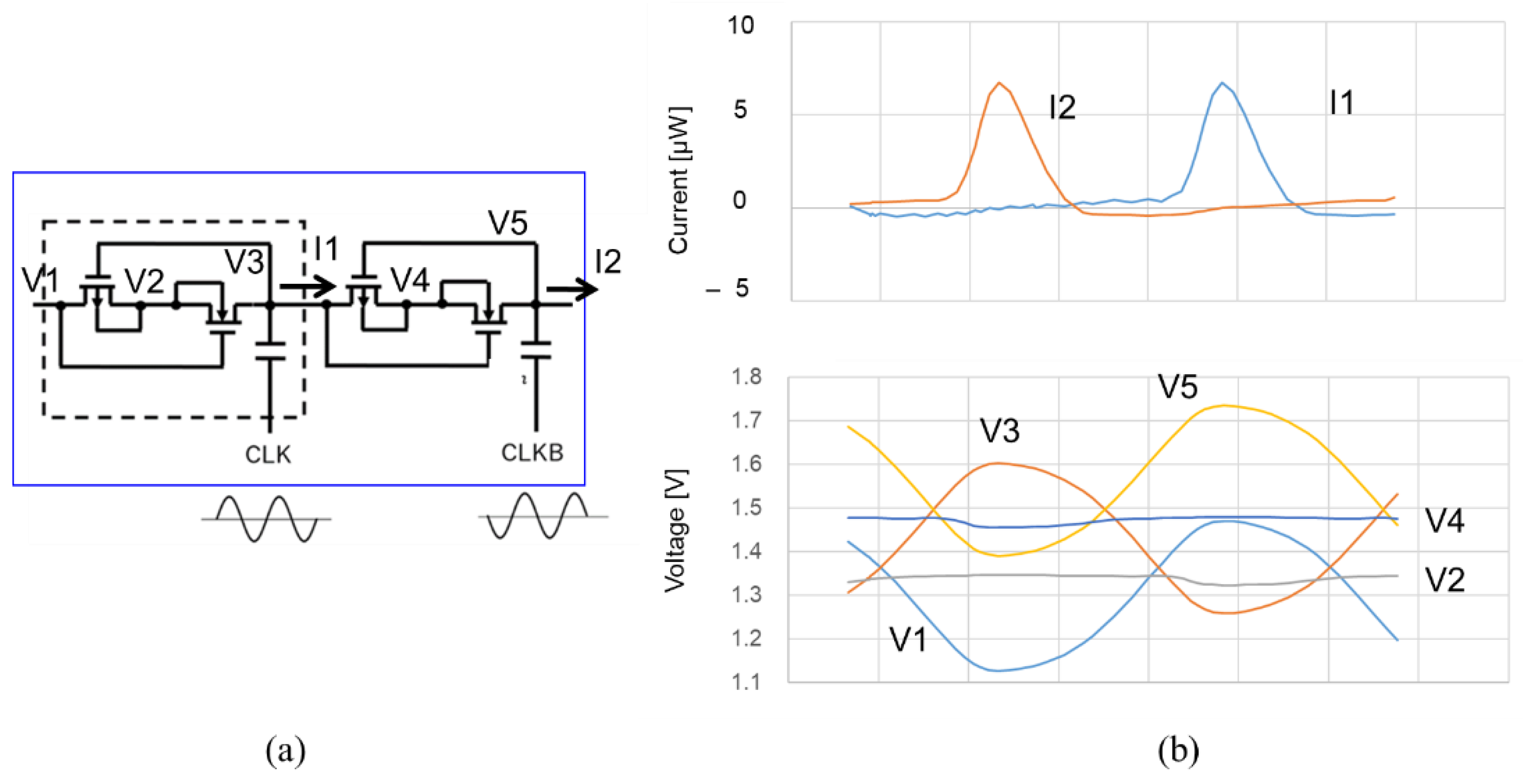
(2-1) Previous model of AC – DC CP [39], [40]
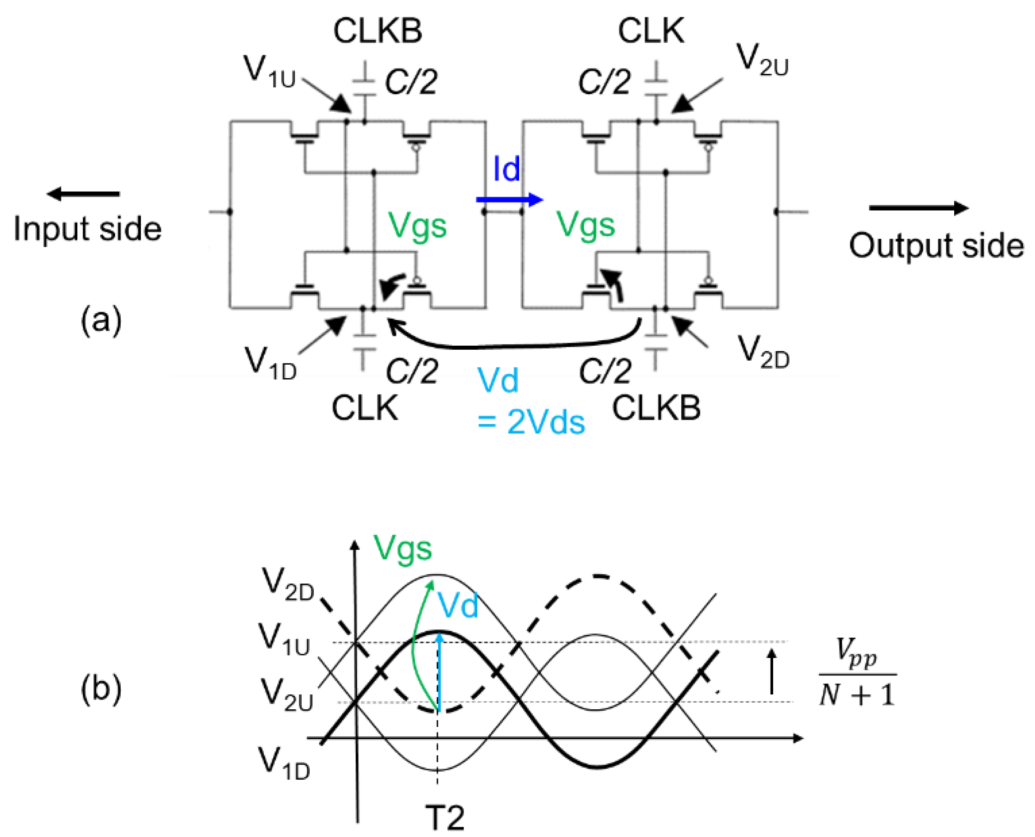
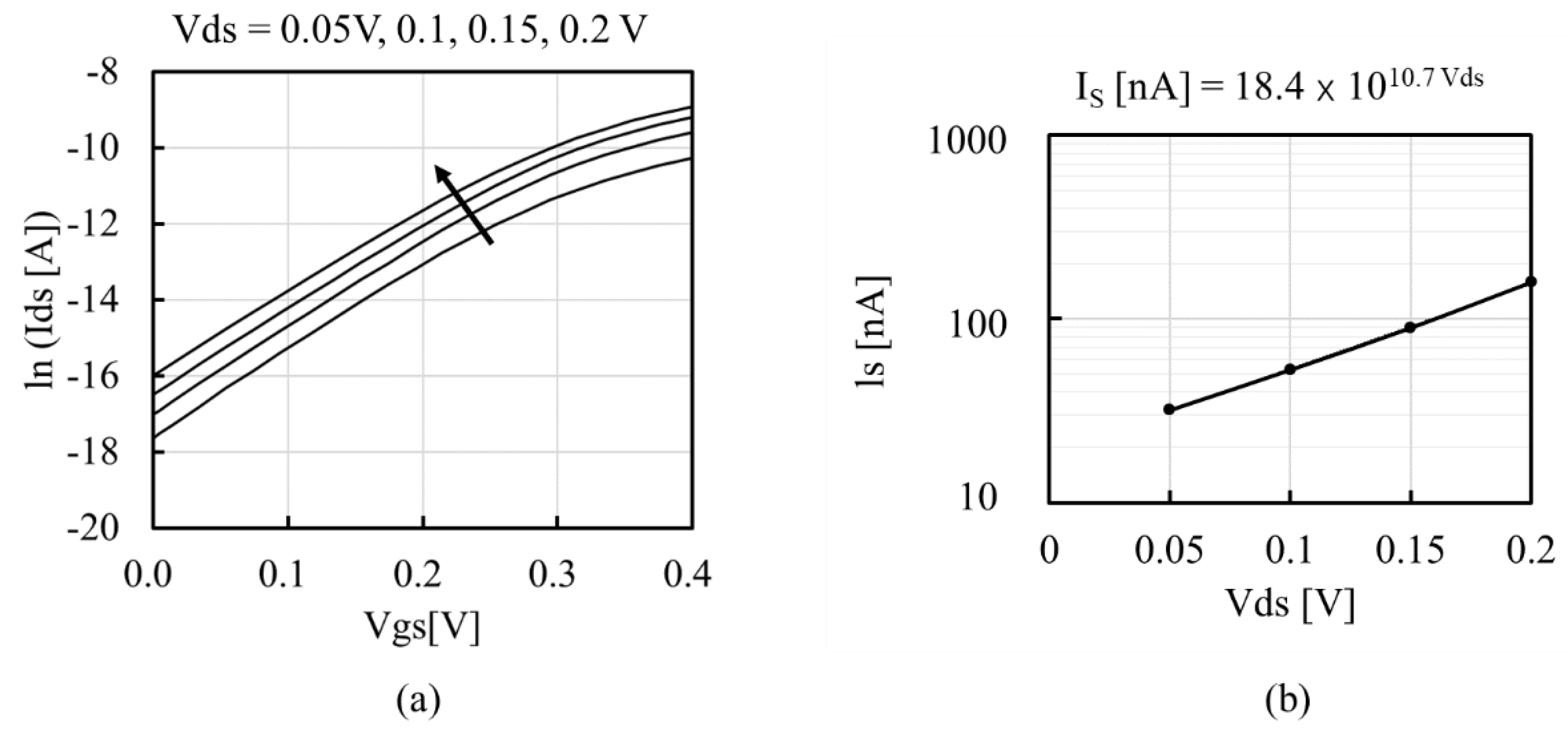
(2-2) Proposed model of XC – CP
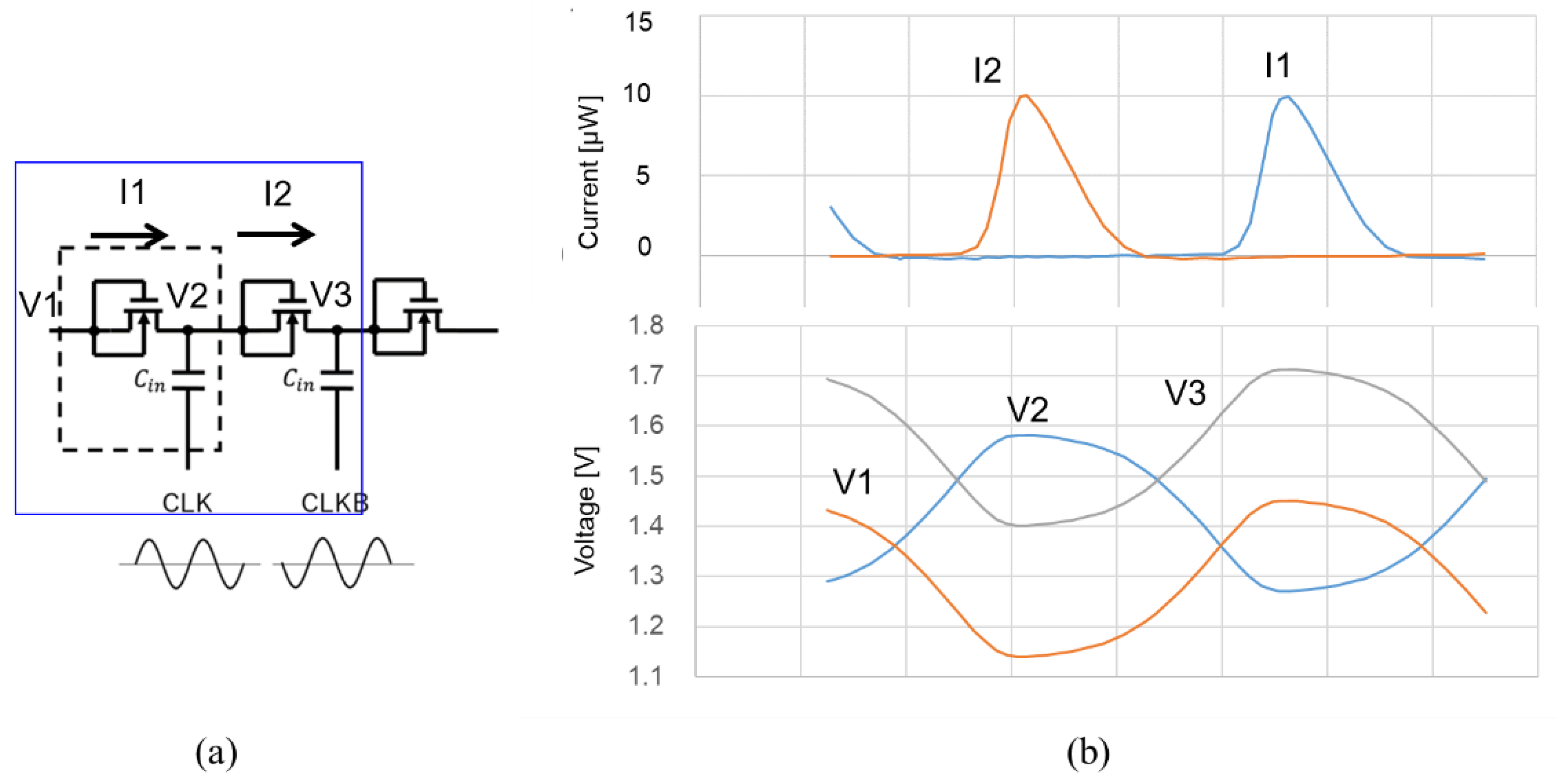
(2-3) More accurate model with a finite output resistance
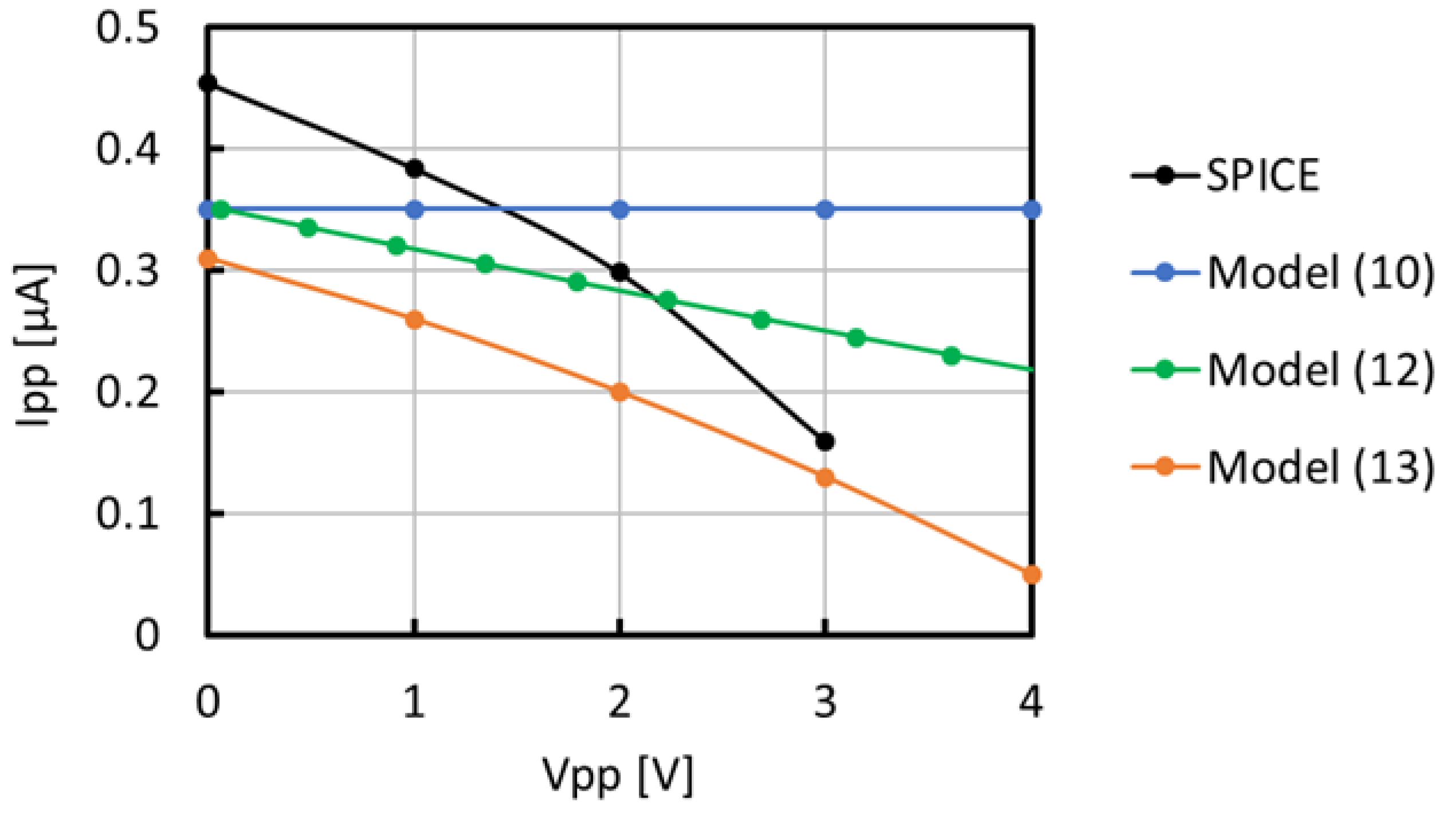
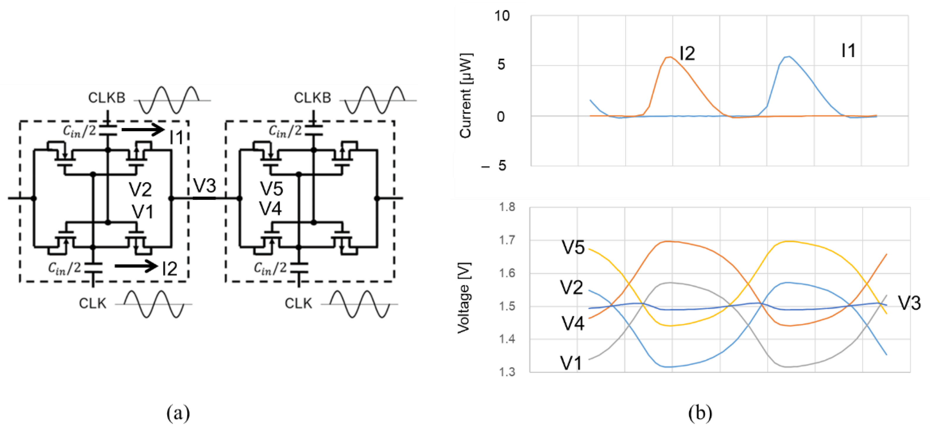
3. Validation of the proposed model
6. Conclusions
Author Contributions
Funding
Data Availability Statement
Conflicts of Interest
References
- Umeda, T.; Yoshida, H.; Sekine, S.; Fujita, Y.; Suzuki, T.; Otaka, S. A 950-MHz Rectifier Circuit for Sensor Network Tags With 10-m Distance. IEEE J. Solid-State Circuits 2006, 41, 35–41. [CrossRef]
- Shetty, D.; Steffan, C.; Bösch, W.; Grosinger, J. Sub-GHz RF Energy Harvester including a Small Loop Antenna. In Proceedings of the 2022 IEEE Asian Solid-State Circuits Conference (A-SSCC), Taipei, Taiwan, 6–9 November 2022; pp. 1–3. [CrossRef]
- Hashimoto, T., Nekozuka, H., Toeda, Y., Otani, M., Fukuoka, Y., & Tanzawa, T. (2023). A− 31.7 dBm Sensitivity 0.011 mm2 CMOS On-Chip Rectifier for Microwave Wireless Power Transfer. Electronics, 12(6), 1400.
- Brown, William C. "The history of power transmission by radio waves." IEEE Transactions on microwave theory and techniques 32.9 (1984): 1230-1242.
- Jabbar, Hamid, Young S. Song, and Taikyeong Ted Jeong. "RF energy harvesting system and circuits for charging of mobile devices." IEEE Transactions on Consumer Electronics 56.1 (2010): 247-253. [CrossRef]
- Valenta, Christopher R., and Gregory D. Durgin. "Harvesting wireless power: Survey of energy-harvester conversion efficiency in far-field, wireless power transfer systems." IEEE microwave magazine 15.4 (2014): 108-120. [CrossRef]
- Yamazaki, Y.; Tsuchiaki, M.; Tanzawa, T. A Design Window for Device Parameters of Rectifying Diodes in 2.4 GHz Mi-cro-watt RF Energy Harvesting. In Proceeding of the 2019 IEEE Asia-Pacific Microwave Conference (APMC), Singapore, 10–13 December 2019; pp. 135–137. [CrossRef]
- McSpadden, James O., and John C. Mankins. "Space solar power programs and microwave wireless power transmission technology." IEEE microwave magazine 3.4 (2002): 46-57. [CrossRef]
- Strassner, Bernd, and Kai Chang. "Microwave power transmission: Historical milestones and system components." Proceedings of the IEEE 101.6 (2013): 1379-1396. [CrossRef]
- Ladan, Shabnam, Ajay Babu Guntupalli, and Ke Wu. "A high-efficiency 24 GHz rectenna development towards millimeter-wave energy harvesting and wireless power transmission." IEEE Transactions on Circuits and Systems I: Regular Papers 61.12 (2014): 3358-3366. [CrossRef]
- Kamada, H., Yang, B., Shao, W., Shinohara, N., & Mitani, T. (2022, November). Application of Partially Driven Array Antenna to 28 GHz Near-Field WPT. In 2022 Asia-Pacific Microwave Conference (APMC) (pp. 255-257). IEEE.
- Lee, H. M., & Ghovanloo, M. (2011, September). Fully integrated power-efficient AC-to-DC converter design in inductively-powered biomedical applications. In 2011 IEEE Custom Integrated Circuits Conference (CICC) (pp. 1-8). IEEE.
- Hashemi, S. S., Sawan, M., & Savaria, Y. (2012). A high-efficiency low-voltage CMOS rectifier for harvesting energy in implantable devices. IEEE Transactions on Biomedical Circuits and Systems, 6(4), 326-335. [CrossRef]
- Li, X., Tsui, C. Y., & Ki, W. H. (2015). A 13.56 MHz wireless power transfer system with reconfigurable resonant regulating rectifier and wireless power control for implantable medical devices. IEEE Journal of Solid-State Circuits, 50(4), 978-989. [CrossRef]
- Noh, K., Amanor-Boadu, J., Zhang, M., & Sánchez-Sinencio, E. (2018). A 13.56-MHz CMOS active rectifier with a voltage mode switched-offset comparator for implantable medical devices. IEEE Transactions on Very Large Scale Integration (VLSI) Systems, 26(10), 2050-2060. [CrossRef]
- Ballo, A., Bottaro, M., & Grasso, A. D. (2021). A review of power management integrated circuits for ultrasound-based energy harvesting in implantable medical devices. Applied Sciences, 11(6), 2487. [CrossRef]
- Beeby, S. P, M. J Tudor, and N. M. White. "Energy harvesting vibration sources for microsystems applications." Measurement science and technology 17.12 (2006): R175. [CrossRef]
- Rahimi, A.; Zorlu, O.; Külah, H.; Muhtaroglu, A. An interface circuit prototype for a vibration-based electromagnetic energy harvester. In Proceedings of the 2010 International Conference on Energy Aware Computing; Institute of Electrical and Electronics Engineers (IEEE), Cairo, Egypt, 16–18 December 2010; pp. 1–4.
- Maurath, D.; Becker, P.F.; Spreemann, D.; Manoli, Y. Efficient Energy Harvesting with Electromagnetic Energy Transducers Using Active Low-Voltage Rectification and Maximum Power Point Tracking. IEEE J. Solid-state Circuits 2012, 47, 1369–1380. [CrossRef]
- Kawauchi, Hayato, and Toru Tanzawa. "A fully integrated clocked AC-DC charge pump for mignetostrictive vibration energy harvesting." Electronics 9.12 (2020): 2194. [CrossRef]
- J. F. Dickson, “On-chip high-voltage generation in MNOS integrated circuits using an improved voltage multiplier technique,” IEEE J. Solid-State Circuits, vol. SSC-11, no. 3, pp. 374–378, Jun. 1976. [CrossRef]
- Oh, Seunghyun, and David D. Wentzloff. "A− 32dBm sensitivity RF power harvester in 130nm CMOS." 2012 IEEE radio frequency integrated circuits symposium. IEEE, 2012.
- Shameli, A., Safarian, A., Rofougaran, A., Rofougaran, M., & De Flaviis, F. (2007). Power harvester design for passive UHF RFID tag using a voltage boosting technique. IEEE Transactions on Microwave Theory and Techniques, 55(6), 1089-1097. [CrossRef]
- D. Levacq, C. Liber, V. Dessard, and D. Flandre, “Composite ULP diode fabrication, modelling and applications in multi-Vth FDSOI CMOS technology,” Solid-State Electron., vol. 48, no. 6, pp.1017–1025, Jun. 2004.
- Szarka, Gyorgy D., Bernard H. Stark, and Stephen G. Burrow. "Review of power conditioning for kinetic energy harvesting systems." IEEE transactions on power electronics 27.2 (2011): 803-815. [CrossRef]
- Schmickl, Stefan, Thomas Faseth, and Harald Pretl. "An RF-energy harvester and IR-UWB transmitter for ultra-low-power battery-less biosensors." IEEE Transactions on Circuits and Systems I: Regular Papers 67.5 (2020): 1459-1468. [CrossRef]
- Gariboldi, R.; Pulvirenti, F. A 70 mΩ Intelligent High Side Switch with Full Diagnostics. IEEE J. Solid-State Circuits 1996, 31, 915–923. https://doi.org/10.1109/4.508203. [CrossRef]
- 28. Kotani, Koji, Atsushi Sasaki, and Takashi Ito. "High-efficiency differential-drive CMOS rectifier for UHF RFIDs." IEEE Journal of Solid-State Circuits 44.11 (2009): 3011-3018. [CrossRef]
- Hwang, Hye-Won, Jung-Hoon Chun, and Kee-Won Kwon. "A low power cross-coupled charge pump with charge recycling scheme." 2009 3rd International Conference on Signals, Circuits and Systems (SCS). IEEE, 2009.
- Palumbo, Gaetano, and Domenico Pappalardo. "Charge pump circuits: An overview on design strategies and topologies." IEEE Circuits and Systems Magazine 10.1 (2010): 31-45. [CrossRef]
- You, K., Kim, H., Kim, M., & Yang, Y. (2011, November). 900 MHz CMOS RF-to-DC converter using a cross-coupled charge pump for energy harvesting. In 2011 IEEE International Symposium on Radio-Frequency Integration Technology (pp. 149-152). IEEE.
- Ballo, Andrea, Alfio Dario Grasso, and Gaetano Palumbo. "A high-performance charge pump topology for very-low-voltage applications." IEEE Transactions on Circuits and Systems II: Express Briefs 67.7 (2019): 1304-1308. [CrossRef]
- Ballo, Andrea, Alfio Dario Grasso, and Gaetano Palumbo. "A review of charge pump topologies for the power management of IoT nodes." Electronics 8.5 (2019): 480. [CrossRef]
- Ballo, A., Grasso, A. D., & Palumbo, G. (2020). A subthreshold cross-coupled hybrid charge pump for 50-mV cold-start. IEEE Access, 8, 188959-188969. [CrossRef]
- G. De Vita and G. Iannacccone, “Design criteria for the RF section of UHF and microwave passive RFID transponders,” IEEE Transactions on Microwave Theory and Techniques, vol. 53, no. 9, pp. 2978-2990, Sep. 2005. [CrossRef]
- J. Yi, W.-H. Ki, and C.-Y. Tsui, "Analysis and design strategy of UHF micro-power CMOS rectifiers for micro-sensor and RFID applications," IEEE Transactions on Circuits and Systems I: Regular Papers, vol. 54, no. 1, pp. 153-166, Jan. 2007. [CrossRef]
- R. E. Barnett, J. Liu, and S. Lazar, “A RF to DC voltage conversion model for multi-stage rectifiers in UHF RFID transponders,” IEEE Journal of Solid-State Circuits, vol. 44, no. 2, pp. 354-370, Feb. 2009. [CrossRef]
- A.J. Cardoso, C. G. Montoro, and M. C. Schneider, “Design of very low voltage CMOS rectifier circuits,” IEEE Circuits and Systems for Medical and Environmental Applications Workshop (CASME), pp. 1-4, Dec. 2010.
- Tanzawa, Toru. "An analytical model of AC-DC voltage multipliers." 2014 21st IEEE International Conference on Electronics, Circuits and Systems (ICECS). IEEE, 2014.
- T. Tanzawa, “An Analytical Model of AC-DC Charge Pump Voltage Multipliers”, IEICE Trans. Electron., vol. E99-C, no.1 Jan, 2016. https://doi.org/10.1587/transele.e99.c.108. [CrossRef]
- Eid, M. H., & Rodriguez-Villegas, E. (2017). Analysis and design of cross-coupled charge pump for low power on chip applications. Microelectronics journal, 66, 9-17. [CrossRef]
- R. Kotsubo, T. Tanzawa, “Modeling of subthreshold operation CMOS Latch-type RF-DC Charge Pump Circuits,” Proceedings of the Electronics Society Conference of IEICE, Mar. 2022. http://hdl.handle.net/10297/00028678.
- 4R. Kotsubo, T. Tanzawa, “The Origin of the Output Resistance in subthreshold Operation CMOS Latch-type RF-DC Charge Pump Circuits,” Proceedings of the Electronics Society Conference of IEICE, Sep. 2022. http://hdl.handle.net/10297/00029107.


| Parameter | Symbol | Value |
|---|---|---|
| Clock frequency | f | 1 GHz |
| Number of stages | N | 32 |
| Stage capacitance | C | 100 fF |
| Clock amplitude | Vdd | 400mV |
| Parameter | Description | Parameter | Description |
|---|---|---|---|
| Frequency of input power | Saturation current of MOSFET operating in subthreshold region | ||
| Input AC voltage of XC–CP | C | Stage capacitor (capacitance per stage) | |
| Amplitude of Vin | Number of stages | ||
| Output DC voltage of XC–CP | Output resistance of CP | ||
| Average output current of XC–CP | ISC | Short circuit current of CP | |
| Effective thermal voltage | VOC | Open circuit voltage defined by RO ISC |
Disclaimer/Publisher’s Note: The statements, opinions and data contained in all publications are solely those of the individual author(s) and contributor(s) and not of MDPI and/or the editor(s). MDPI and/or the editor(s) disclaim responsibility for any injury to people or property resulting from any ideas, methods, instructions or products referred to in the content. |
© 2023 by the authors. Licensee MDPI, Basel, Switzerland. This article is an open access article distributed under the terms and conditions of the Creative Commons Attribution (CC BY) license (http://creativecommons.org/licenses/by/4.0/).


