I. Introduction
In the realm of photovoltaic (PV) applications, copper-indium-gallium-selenide (Cu(In,Ga)Se
2, CIGSe) stands out as a promising absorber material, characterized by its near-optimal bandgap, high optical absorption coefficients, and long-term stability [
1]. Several studies have reported enhanced solar cell efficiency through the utilization of a CIGSe absorber in conjunction with various buffer layer materials [
2,
3,
4,
5]. In a CIGSe structure, when light enters the absorber layer, photons with energy according to their bandgap values can be absorbed by the absorbing layer as much as possible, thus reducing the amount of light loss [
6]. The bandgap of CuIn
1-xGa
xSe exhibits the lowest value (
Eg=1.02 eV) when
x = 0 and the highest value (
Eg=1.68 eV) when
x = 1 [
1]. The structure and physical properties of CIGSe films are influenced by inherent defects [
7], underscoring the importance of minimizing stoichiometry deviation in the film fabrication process. To achieve a high-quality single-phase chalcopyrite film, optimization of process parameters, such as sputtering powers, is essential. However, there is growing recognition of the impacts of addressing environmental issues and human health. While the buffer-CdS material in CIGSe-solar cells achieves a higher efficiency of 23.82% [
3], it is noteworthy that these Cd-containing materials are environmentally hazardous and raise concerns for ecological impact.
The two-segment process is devised with dual primary objectives: to improve the internal/external quantum efficiencies (IQE and EQE) within the short-wavelength range and to augment the photocurrent and power-conversion efficiency (
η) of flexible CIGSe solar cells. Beyond these objectives, our investigation extends to the exploration of metal-alloy compositions as an alternative to CdS-buffer for environmental sustainability [
8]. From a perspective of environmental consciousness and sustainability, the developed eco-friendly PV modules demonstrate potential for effective application in commercial mass production.
For the CIGSe-solar cell fabrication in this study, the absorber film was prepared by different sputtering powers in the segment-I process, which can effectively adjust the ratios of the [Cu]/([Ga]+[In]) (CGI) and the Ga/(In+Ga) (GGI) values.
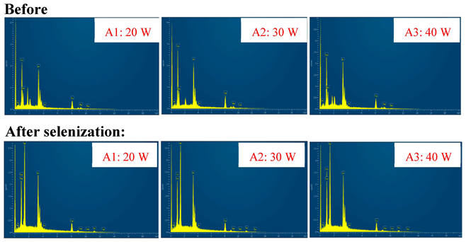
Table 1 provides a summary of the surface composition along with corresponding energy-dispersive X-ray spectroscopy (EDS) spectra images of the absorber films, thus facilitating an investigation into the selenization characteristics of the CIGSe absorbers. Before selenization process (upper half of
Table 1), the CGI ratios of sample A1 (20 W), A2 (30 W) and A3 (40 W) were separated for 0.812, 1.055 and 0.864; while corresponding for 0.649, 0.950 and 0.634, respectively after selenization process (lower half of
Table 1). This procedure exemplifies considerable potential in enhancing the crystallinity of CIGSe films deposited at lower temperatures.

Surface characterization of the CGISe film was performed using an atomic force microscope (AFM) instrument (Bruker INNOVA SPM). A scanning area of 2.5×2.5 mm² (512×512 pixels) was analysed on a vibration-free platform. The root-mean-square (RMS) surface-roughness values (Rq) were determined using the accompanying software of the AFM instrument. Additionally, the optical and electrical properties of the cells were evaluated using commercially available systems, including scanning electron microscopy (SEM) and energy-dispersive X-ray spectroscopy (EDS) (Model: JSM-6500F, JEOL Ltd.), a power-conversion efficiency measuring system (Model: Oriel-91192/AM 1.5 GMM), and overall IQE and EQE measurements (Model: QE-R, Enlitech). The CGI optimal ratio (composite-ratio film) was found to be 0.95, aligning with results reported in the literature [
9].
II. Experiments and Measurements
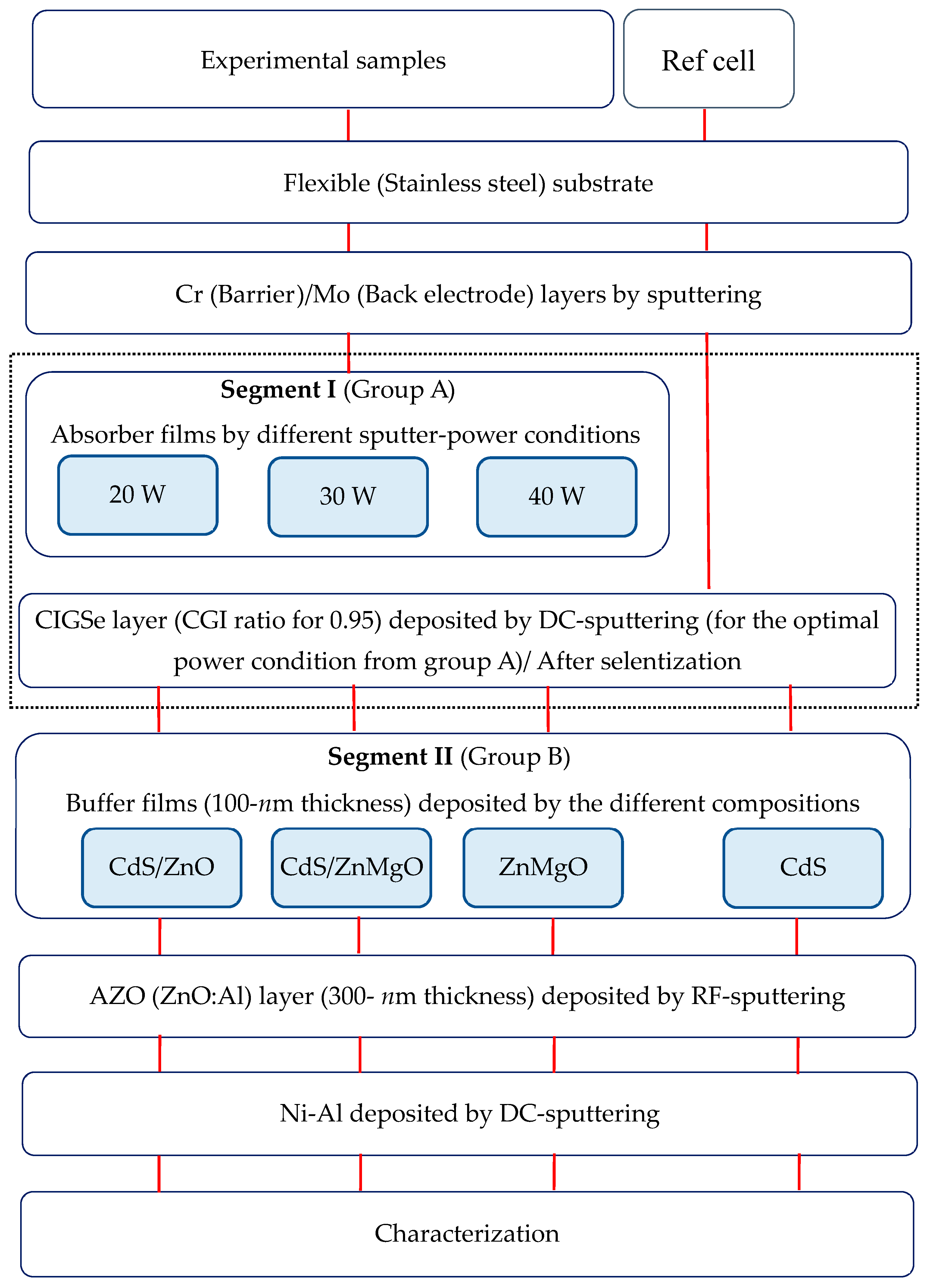
Figure 1 illustrates the process flowchart for fabricating the proposed flexible CIGSe-based solar cells using a two-segment process under varied conditions. Under the Cr barrier/Mo back electrode/stainless-steel (flexible) substrate in the segment-I process at temperature of 550 °C, the micro-film absorbers were made with different RF sputtering powers (20, 30 and 40 W for Group A samples) to seek the optimal sputtering-power condition. Next for the optimal bandgap structure in the segment-II process, buffer films (100-
nm thickness) were made of different metal-alloy compositions (
i.
e., CdS/ZnO, CdS/ZnMgO, ZnMgO and CdS for Group B samples) as the CdS-buffer alternative for the eco-friendly environment. Finally, the completed AZO (ZnO:Al for 300-
nm thickness)/front electrode (Ni-Al) was DC sputtered for characterization analysis.
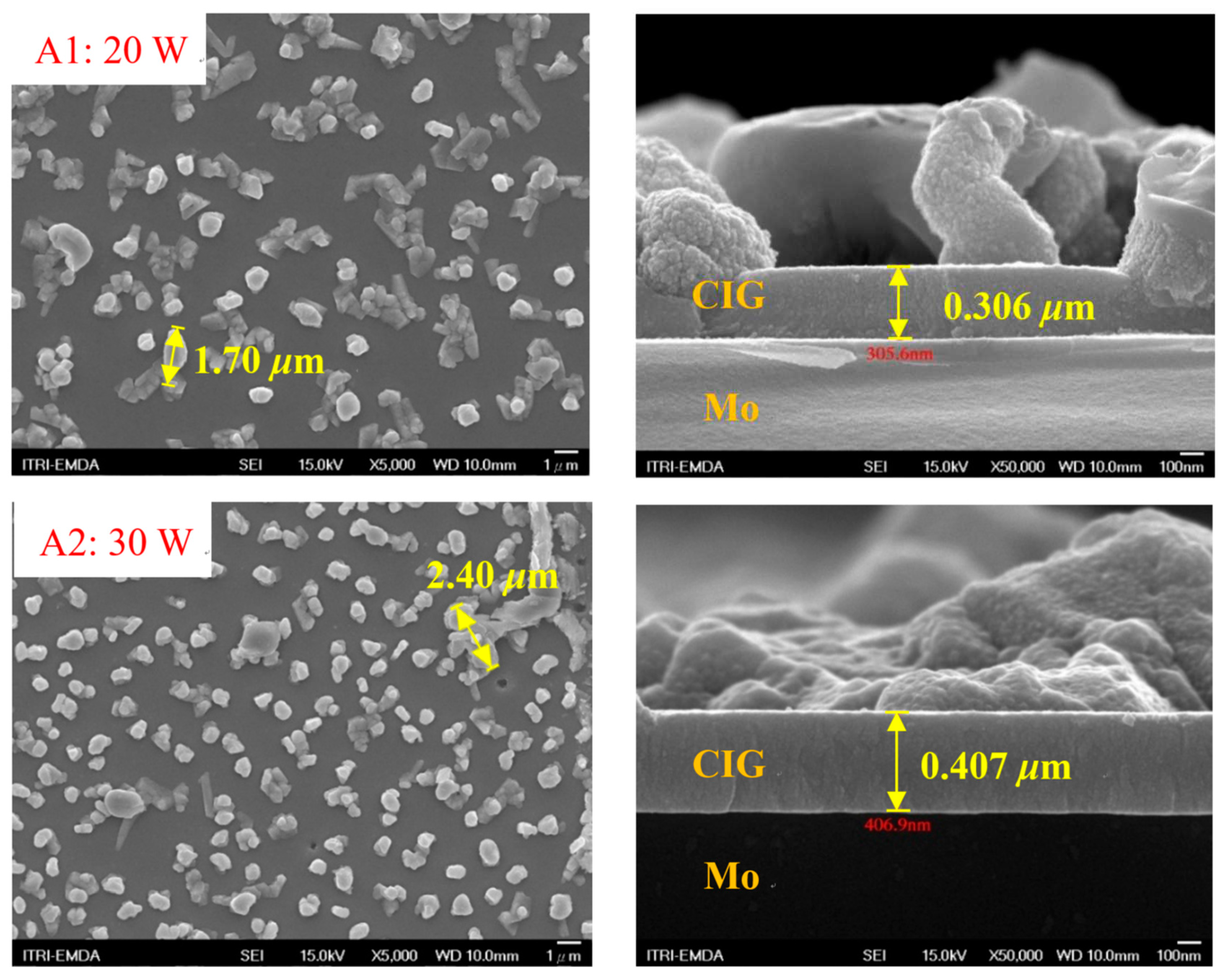
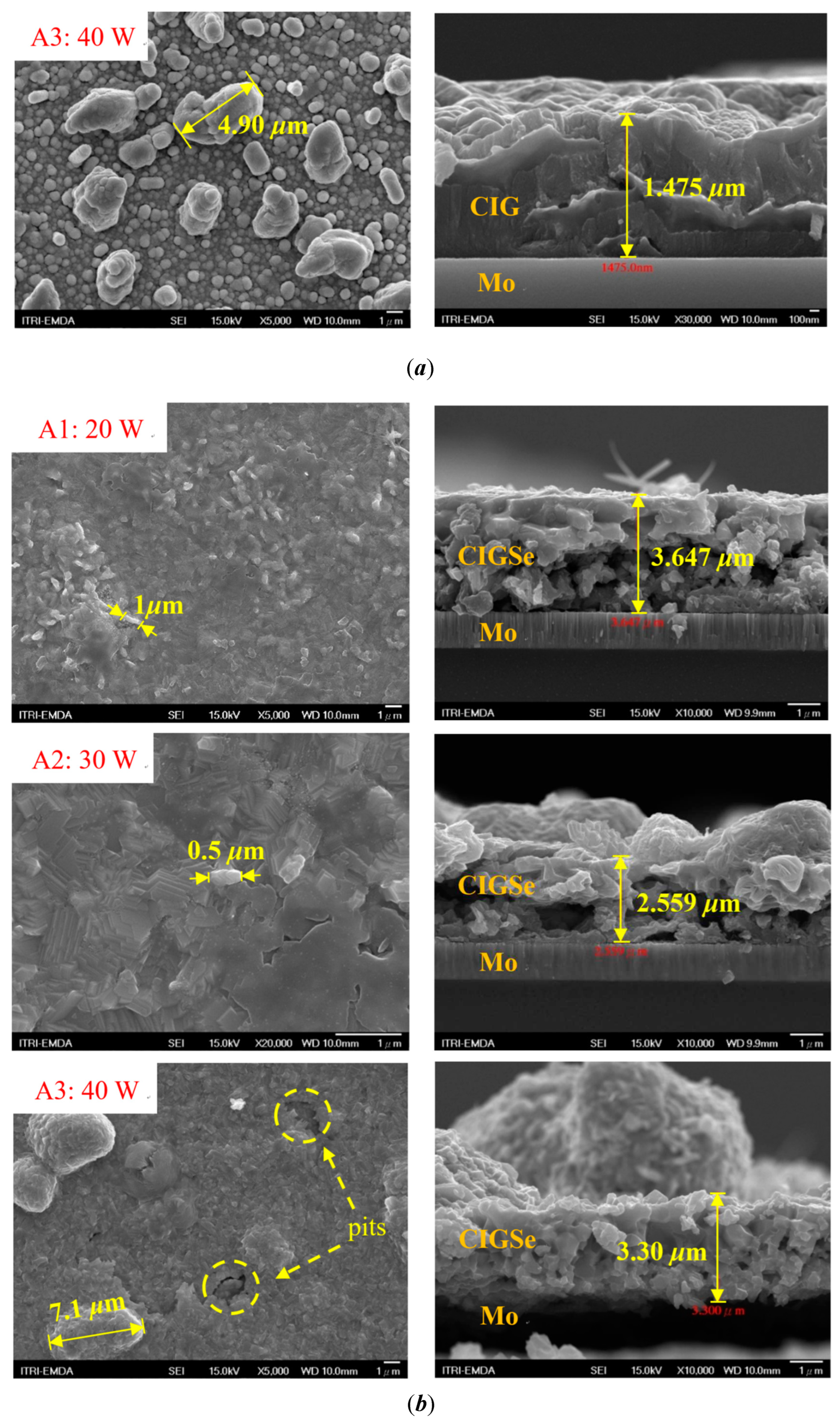
Figure 2 presents SEM images, featuring both top-view (left) and cross-sectional (right) perspectives, obtained subsequent to the segment-I process for CIGSe absorbers under varying sputtering powers (A1: 20 W, A2: 30 W, A3: 40 W). The images are provided for both (
a) before- and (
b) after-selenization stages. Visual inspection suggests that the grain size is larger for the higher sputtering powers even before and after selenization. The surface morphology of each CIGSe absorber is primarily dominated by the underlying particulate structure, even if this microfilm is still visible beneath the covering layer [
10]. Before the CIG film is selenized, the film images of left-
Figure 2(a) have many lumpy structures, and its particulate size gradually increases as the sputtering power gradually increases (20–40 W). After the CIG film is selenized at high sputtering power (40 W) of left-
Figure 2(b), uneven pits are formed on the surface of the film.
At the same time, the thickness of the absorber of Sample A1 (0.306
μm of right-
Figure 2(a)) is thinner than that of sample-A3 absorber (1.475
μm of right-
Figure 2(a)). Additionally, quantification based on the EDS spectra of CIGSe films reveals distinct sputtering powers of 20, 30, and 40 W for samples A1, A2, and A3, respectively (as detailed in
Table 1). Following the selenization of the CIG film, a slower reaction and growth rate occur, leading to the formation of uniform nanoparticles [
11]. Moreover, the inclusion of Cu-rich content, as observed in sample A2 with a 0.95-CGI ratio, within the CIGSe-absorber microfilm distinctly promotes grain growth, and diminishes the presence of fine-grain film, thereby resulting in a substantial improvement in absorber crystallinity and a reduction in trap state density [
12].
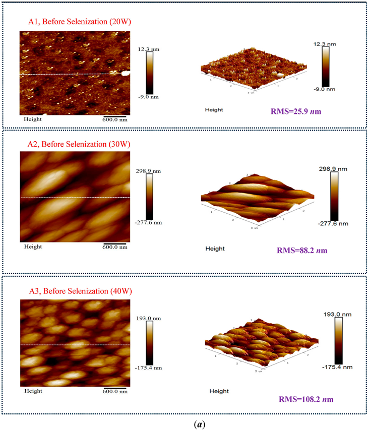
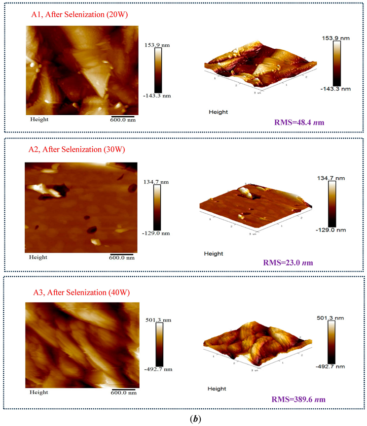
Table 2 plots for 2-D and 3-D AFM images of CIGSe thin-film absorbers prepared by segment-I process. The Ra and Rmax values of samples A1 (20 W), A2 (30 W) and A3 (40 W) were separately for (
a) 17.0/366, 71.8/480 and 80.0/520
nm before selenization, while (
b) 40.2/336.0, 10.5/320.0 and 379.5/682.6
nm after selenzation. Herein, Rmax and Ra denote the maximum surface-height and average center-line roughness, respectively. As depicted in the A2 image post-selenization (
Table 2(b)), a discernible compact and flat surface structure is observed, comprised of cone-shaped columns randomly distributed over the film’s surface. Consequently, the film presents a rough and porous surface, with an RMS surface roughness (Rq) measuring 23.0
nm. These observations are consistent with prior literature [
13], indicating that a more porous film structure produced with a 30 W sputtering power leads to the smallest grain size (~0.5
μm) from
Figure 2.
As mentioned above, the aim of this work is to improve overall efficiencies of
η, IQE and EQE values of the developed flexible CIGSe cell in the ultraviolet (UV)-visible wavelength region. Upon choosing the optimal-30-W CIGSe-absorber sputtered by the segment-I process, we shall consider CIGSe-absorber/buffer bandgap diagrams for the light-absorption as much as possible, thus reducing the amount of light loss [
6]. In the next segment-II process, buffer layers (100-
nm thickness) are made of different micro-film compositions (CdS/ZnO, CdS/ZnMgO, ZnMgO and CdS for Group B samples). Though the electrical resistivity of the microfilm increases with magnesium (Mg) content [
14], therefore, the Zn
1-xMg
xO buffer films were RF-sputtering prepared from ternary-alloy target for adjusting Mg content to satisfy the purpose of optical-bandgap application. Thus, the Tauc function is used to determine the optical bandgap (
Eg in eV) of either disordered or amorphous semiconductors [
15]. When a material is exposed to incident light and acquires sufficient energy to generate a photoelectron, the energy (along with its corresponding wavelength) of the photoelectron follows the principles outlined by the photoelectric effect equation [
16]. This equation is expressed as:
where
α is the absorption coefficient; A is a constant reflecting the extent of band tailing and
hν is the incident photon energy. Obviously, the energy bandgap of Zn
1-xMg
xO film is defined in terms of Mg concentration can be calculated from Eq. (2). Therefore,
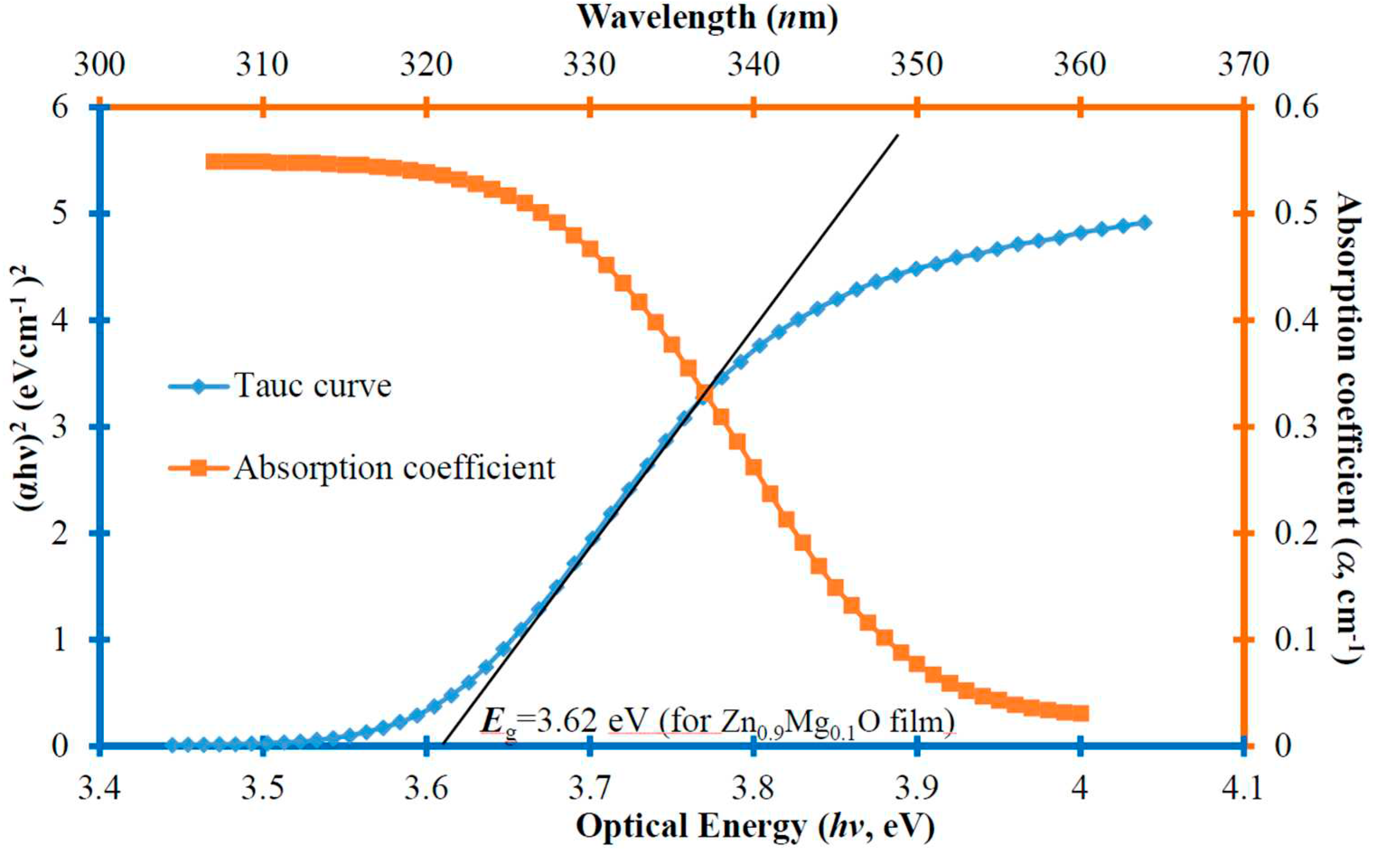
Figure 3 illustrates the comparisons of the optical-energy diagram (
hν in eV) of Zn
1-xMg
xO thin film with Tauc function (Eq.(1)) and absorption coefficient (
α in cm
-1), incorporating of Mg content (Eq.(2)) for the optimal optical-bandgap application. Furthermore, the corresponding value of
Eg (3.62 eV for
x=0.1 in Zn
1-xMg
xO film) is determined by extrapolating the linear portion of the curve to the
hν axis, where (α
hν)
1/2 = 0, as depicted in
Figure 3. This finding is in accordance with the results presented by Singh et al. [
14].
The current density-voltage (
J-
V) characteristics of the flexible-CIGSe cells (with optimal CGI ratio=0.95 from literature [
9]) were experimentally determined under illumination with the conditions of AM1.5G and an irradiance of 1000 W/cm
2.
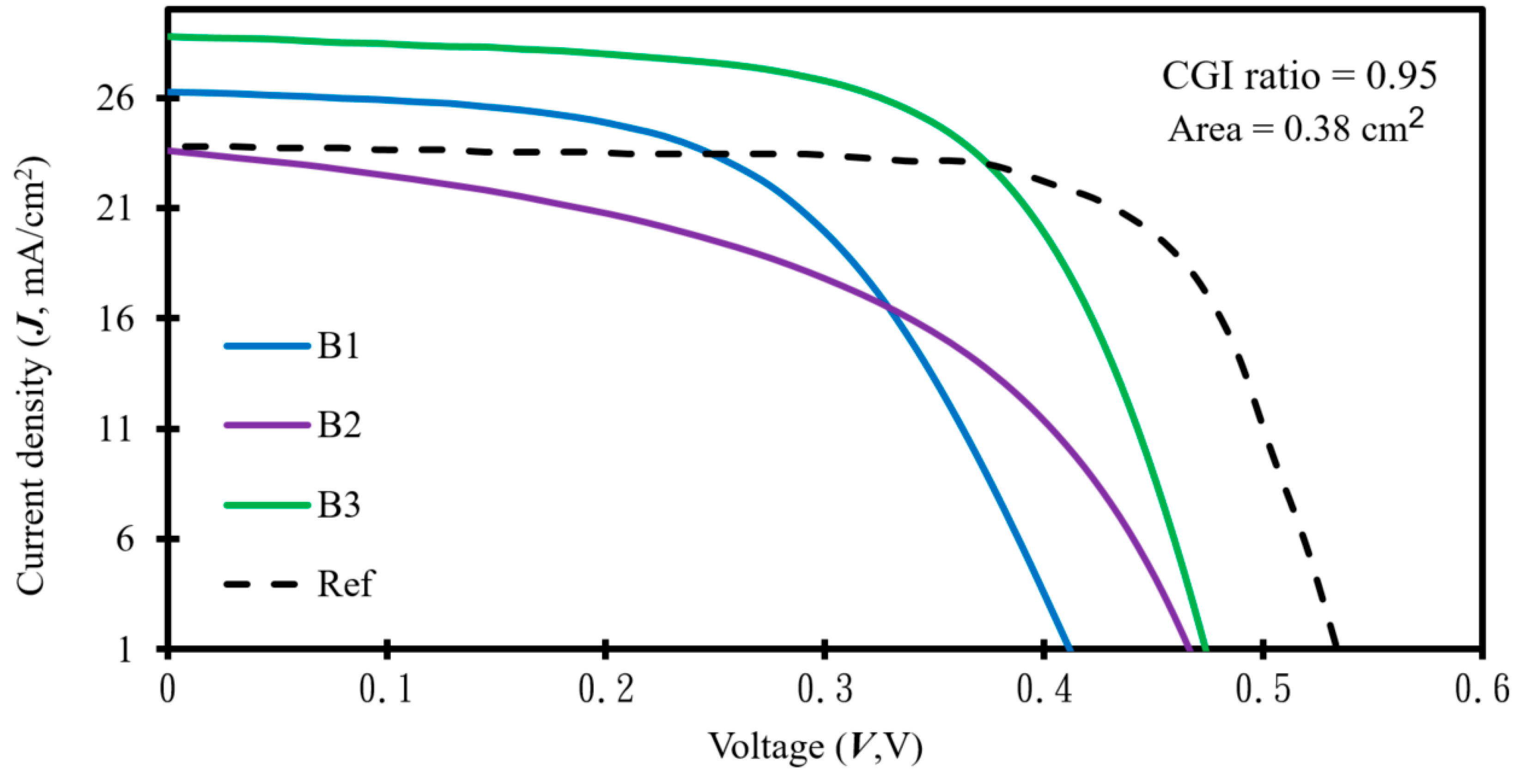
Figure 4 plots the
J-
V curve under illumination, and the electrical properties of the CIGSe-layer solar cells are succinctly presented on the top. The optimal performance was observed in sample B3, featuring a ZnMgO buffer material, resulting in the highest efficiency for the CGISe-layer solar cell. This configuration exhibited a short-circuit current (
JSC) of 28.75 mA/cm², open-circuit voltage (
VOC) of 480
mV, series resistance (RS) of 8 Ω-cm², and a conversion efficiency (
η) of 8.70%. This represents a significant absolute gain of 1.68% compared to the B2 cell. Further investigation revealed that the synthesis technique for the lower Mg-content device (utilizing Zn
0.9Mg
0.1O film) addressed an approximate 3.62-eV-bandgap phenomenon observed in the CIGSe-buffer layer at the optical-band spectra (refer to
Figure 3), as discussed previously. This improvement in optoelectronic quality enhances photon penetration into the buffer layer [
17].
| Samples / Buffer-layer materials |
VOC
(mV) |
JSC
(mA/cm2) |
F.F.
(%) |
η
(%) |
RSh
(Ω-cm2) |
RS
(Ω-cm2) |
|
B1, CdS+ZnO |
480 |
28.05 |
64 |
8.63 |
1042 |
8 |
|
B2, CdS+ZnMgO |
440 |
26.47 |
60 |
7.02 |
1117 |
10 |
|
B3, ZnMgO |
480 |
28.75 |
64 |
8.70 |
827 |
8 |
|
Ref, CdS |
531 |
24.61 |
62.4 |
8.15 |
1615 |
11.1 |
The two-segment process aims to achieve dual objectives: enhancing the internal/external quantum efficiencies (IQE and EQE) in the short-wavelength region, and augmenting the photocurrent and power-conversion efficiency (
η) of flexible CIGSe solar cells. Concurrently, we investigated the feasibility of micro-film compositions as an environmentally friendly alternative to CdS-buffer [
8]. Examining the optoelectrical parameters depicted in
Figure 4, the short-circuit current density (
JSC), incident light power (
PL), optical bandgap (
Eg), and reflectance (R(
λ)) were utilized to calculate the local IQE with respect to wavelength (IQE(
λ)) using the following equation [
18]:
Referred hereafter as Ref and sample-CIGSe cells,
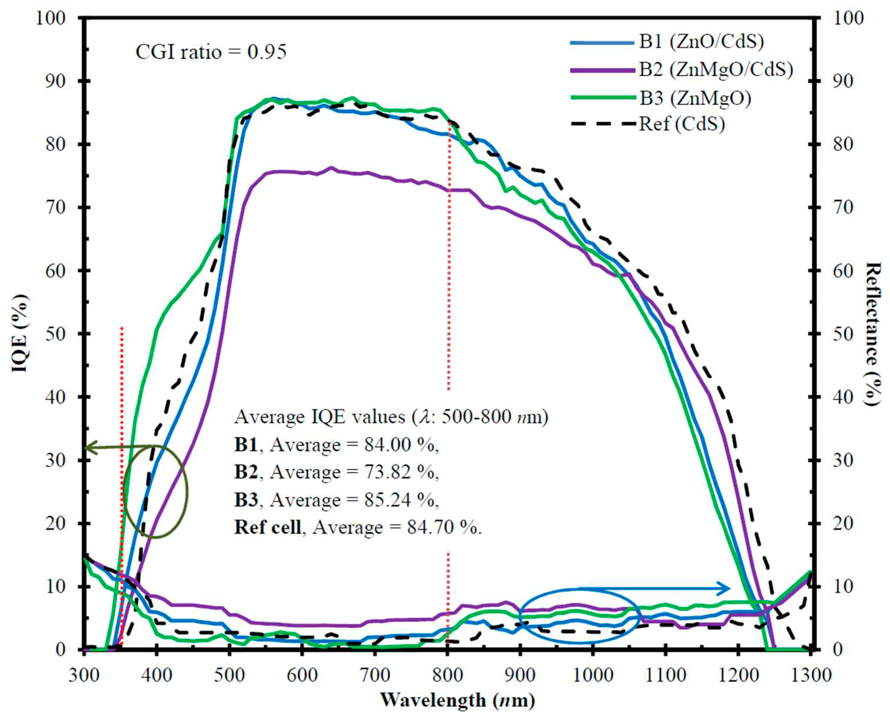
Figure 5 presents the IQE values (Eq. (3)) and the corresponding reflectance (R(
λ) measured at the 300–1,300
nm wavelength radiation) for different micro-film compositions (B1: CdS/ZnO, B2: CdS/ZnMgO, B3: ZnMgO and Ref: CdS). In which, the IQE curve of sample B3 (Average value=85.24% with ZnMgO-buffer cell) is higher than those of other cells in a visible range (500–800
nm wavelength). Moreover, the measured R(
λ) and the IQE values are fitted simultaneously to account for the dependence of the electrical performance on the optical properties (top chart in
Figure 4) of the cell. In which for sample B3, the
JSC value depends on the buffer-film bandgap, and
JSC has higher value to satisfy the Mg-content composition, thus resulting in higher
η values. Hence, the increased IQE has led to reduced reflectance in the longer wavelength range. Meanwhile, the decrease in IQE at shorter wavelengths (below 500
nm) can be attributed to surface recombination, aligning with the findings in the study by Cheng et al. [
19].
In the meantime,
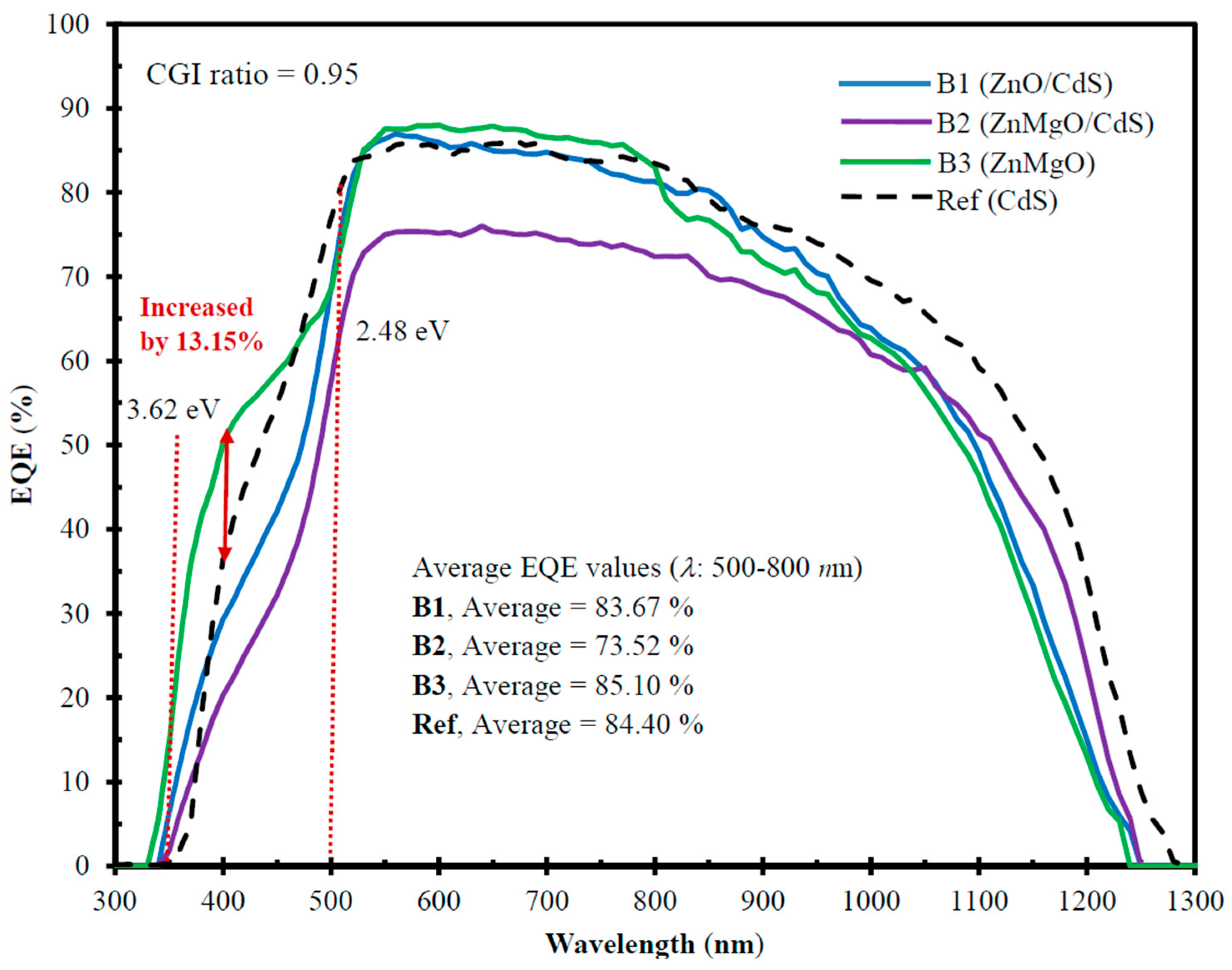
Figure 6 illustrates the spectral-EQE curves in a wide-wavelength range (300–1300
nm) of the developed three samples and Ref cell. In this study, the EQE of the developed samples are lower than those of the Ref cell for all wavelengths. For the short-wavelength range (350–500
nm corresponding band gap for 3.62–2.48 eV), it should be noted that the average EQE value of sample B3 was greater than that of Ref cell by 13.15%, thus contributing to the band-gap (
Eg=3.62 eV) effectiveness for the optimal Zn
0.9Mg
0.1O-content buffer and Mo as a back surface layer as a hole transport-electron reflected layer [
3].
In the long range of wavelengths (500–800
nm), the average EQE values are 83.67%, 73.52%, 85.10%, and 84.40% for samples B1, B2, B3, and Ref cell, respectively. For a Ga-grading bandgap at the back side, Mo provides a sufficient self-passivation at the absorber/back contact interface [
20]. This indicates a clear self-passivation quality improvement, which quasi-ohmic electrical contact overcomes Mo-diffusion effect on CIGSe/Mo interfaces. The sample B3 shows the most desirable average for the area under the curve (85.10%), thus it has the highest value of
F.
F. and the highest conversion efficiency (
η=8.70%) as seen in
Figure 4. In the proposed two-segment process, we had enhanced the performance of overall efficiencies by optimizing the cell parameters in terms of RF sputtering powers for CIGSe-absorber layer, and Mg-concentration of Zn
1-xMg
xO-buffer film. In which, the Cd-alternative buffer layer not only improves the device efficiency owing to better light absorption [
21], but also satisfies the environmental requirement for Cd-usage reduction.
Set up from nine optimal CIGSe-solar cells (sample B3) for the dimension of 30 × 30-cm
2 area, the PV-array module has been connected to a variable load (rheostat of 220 Ω, and 10 A) through multi-meters for current and voltage measurement.
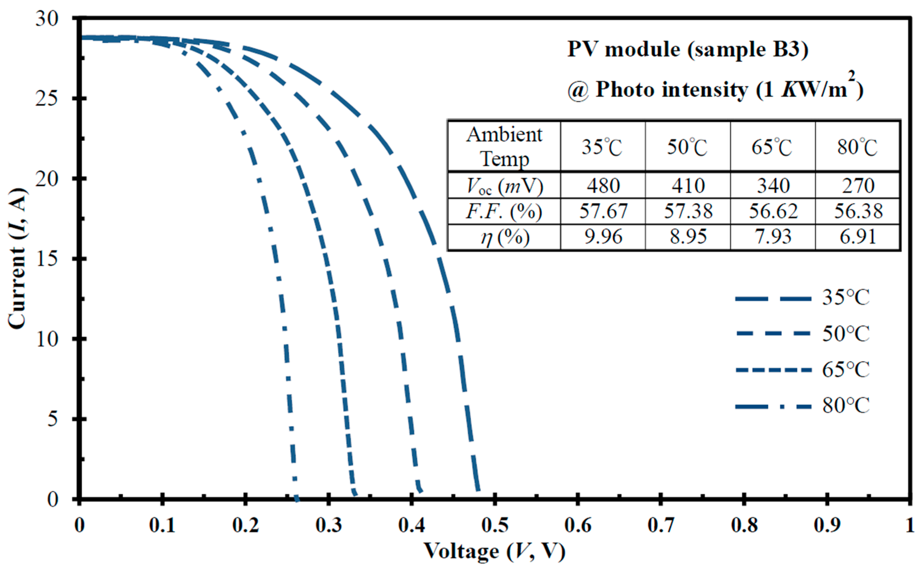
Figure 7 illustrates the current (A)-voltage (V) curves of a PV module under a photo intensity of 1
KW/m
2, showcasing the impact of varying ambient temperatures. Notably, the
VOC experienced a decrease (from 480 to 270
mV) as the ambient temperature rose from 35 to 80 °C. Corresponding optoelectrical performance parameters (
VOC, fill factor (
F.
F.), and η values) for the developed PV module at these ambient temperatures are provided in the upper portion of
Figure 7. As the temperature increases, the optical bandgap of the semiconductor contracts, causing a reduction in the
VOC value in accordance with the temperature dependence of the p–n junction voltage from the Tauc function, as previously described in Eq. (1). This negative-temperature effect on the
VOC value results in a decline in its
η value (from 9.96% to 6.91%), aligning with similar observations reported in [
9].
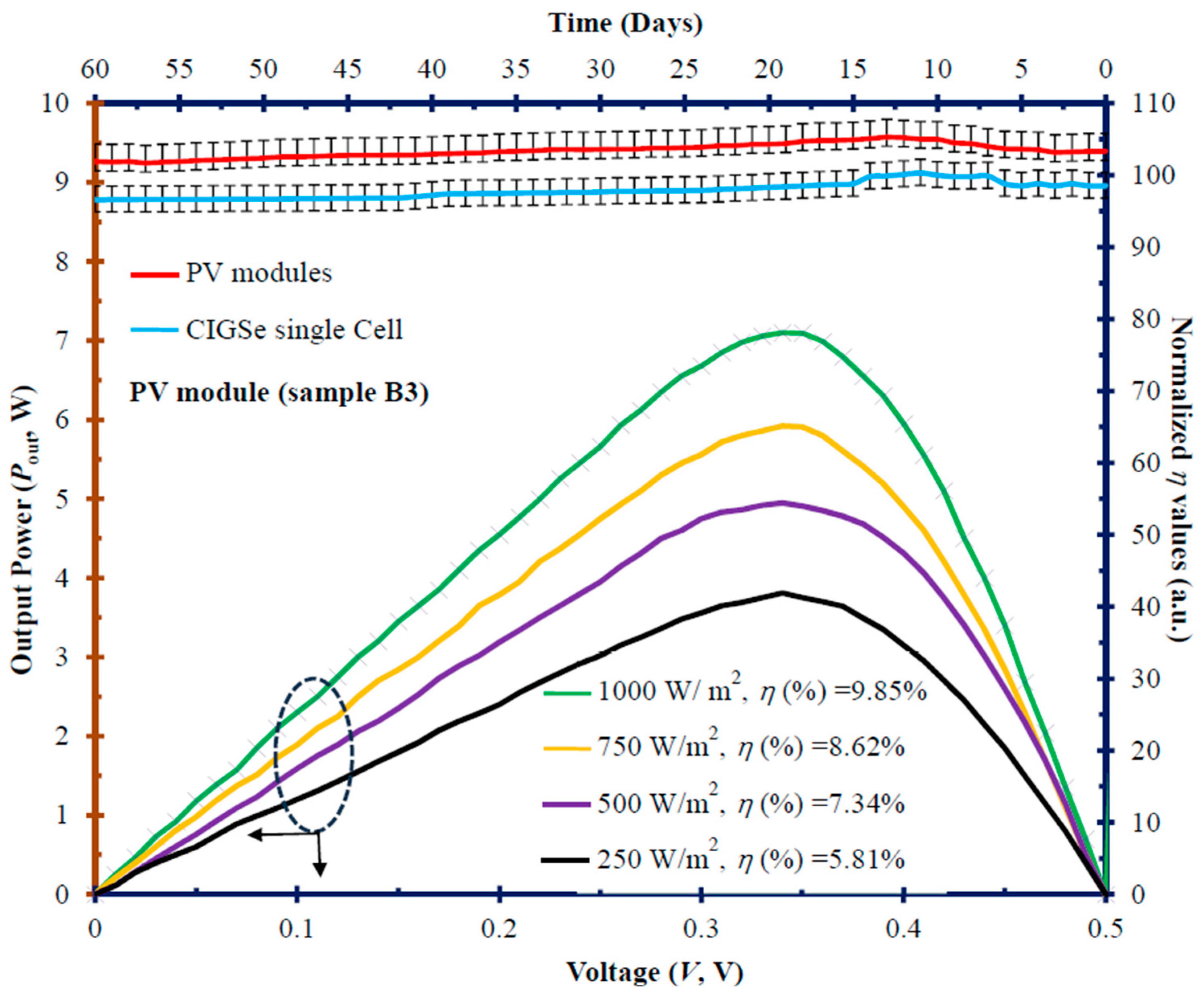
At a constant ambient temperature of 25 °C, the optimal CIGSe solar cells within a PV module (sample B3) exhibit a linearly increasing output power-voltage (
Pout-V) relationship, as depicted in
Figure 8. This trend is observed with a gradual elevation in the photo intensity from 250 to 1000 W/m
2. Conversely, this illustrates the positive impact of photo intensity on the
VOC value, consequently resulting in an enhancement of its
η value (from 5.81% to 9.85%). This observation aligns with the findings reported in [
22].
Concurrently,
Figure 8 displays the stability curves of the normalized
η values measured over a 60-day period. The data were normalized to the initial performances of the as-grown cell/module without adjustments for irradiance levels [
23]. Consequently, the day and night cycles are manifested in the data. The error bars associated with each data point represent the range between the maximum and minimum values observed for both the PV module and CIGSe single cell at each specific data point. All varied by less than ±5% of
Figure 8 (on the top-right axis), the developed PV module and CIGSe-single cell assess the acceptable
η-value stability, which is the same argument with the literature [
24].
Figure 1.
The overall flow chart of CIGSe solar cells by two-segment process. Under the Cr barrier/Mo back electrode/stainless-steel (flexible) substrate in the segment-I process, the absorption layer is made with different sputtering powers. Next in the segment-II process, buffer layer is made of different microfilm compositions (CdS/ZnO, CdS/ZnMgO, ZnMgO and CdS for Group B samples). Lastly, AZO (ZnO:Al for 300-nm thickness)/front electrode (Ni-Al) was sputtered for comparison and analysis.
Figure 2.
The SEM images of the CIGSe-absorber microfilms after segment I process. The top view (left) and cross-sectional view (right) were sputtered at different powers (A1: 20 W, A2: 30 W, A3: 40 W), respectively. (a) Before selenization with particulate size (from 1.7 to 4.9 μm) corresponding with thickness (from 305.6 to 1475 nm), (b) After selenization with particulate size are separately for 1 μm (A1), 0.5 μm (A2), 7.1 μm (A3) corresponding with thickness are for 3.647 μm (A1), 2.559 μm (A2), 3.3 μm (A3), respectively.
Figure 3.
The optical-band diagram (hν in eV) of Zn1-xMgxO thin film with a comparison of Tauc curve [(αhν)2 in (eV cm-1)2, bottom-left axis] and absorption coefficient (α in cm-1, corresponding with wavelength on the top-right axis) of CIGSe–solar cells. For the Mg content (x=0.1) of the Zn1-xMgxO film, the value of Eg is 3.62 eV.
Figure 4.
The current density-output voltage (J-V) curves were generated using various buffer-layer materials (CdS/ZnO, CdS/ZnMgO, ZnMgO, CdS) for samples B1, B2, B3, and the Ref cell. The optoelectrical performance of CIGSe-solar cells is presented above the corresponding curves.
Figure 4.
The current density-output voltage (J-V) curves were generated using various buffer-layer materials (CdS/ZnO, CdS/ZnMgO, ZnMgO, CdS) for samples B1, B2, B3, and the Ref cell. The optoelectrical performance of CIGSe-solar cells is presented above the corresponding curves.
Figure 5.
Spectral optoelectronic comparison of internal quantum efficiency (IQE in %, bottom-left axis) and reflectance (R(λ) in %, bottom-right axis) for wavelengths from 500 to 800 nm of CIGSe-solar cells (for CGI optimal ratio approaches 0.95) prepared with different buffer-layer materials (CdS/ZnO, CdS/ZnMgO, ZnMgO, CdS) for samples of B1, B2, B3 and Ref cell.
Figure 6.
The external quantum efficiency (EQE in %) of CIGSe-solar cells prepared with different buffer-layer materials (CdS/ZnO, CdS/ZnMgO, ZnMgO, CdS) for samples of B1, B2, B3 and Ref cell.
Figure 6.
The external quantum efficiency (EQE in %) of CIGSe-solar cells prepared with different buffer-layer materials (CdS/ZnO, CdS/ZnMgO, ZnMgO, CdS) for samples of B1, B2, B3 and Ref cell.
Figure 7.
Under a constant irradiance level (KW/m2), the current-voltage (I–V) curves were captured for a PV module consisting of nine optimal CIGSe-solar cells (sample B3) at varied ambient temperatures (35–80 °C). Additionally, the optoelectrical performance of the PV system is depicted in the top inset.
Figure 8.
At a constant ambient temperature of 25 °C, output power-voltage (Pout-V) curves were generated for optimal CIGSe-solar cells prepared within a PV module (sample B3). These curves were observed across a range of photo intensities (250–1000 W/m2) [bottom-left axis]. Additionally, the corresponding stability curves of normalized efficiency values (η) (a.u., corresponding with time (days) on the top-right axis) are provided for both the PV module and a single CIGSe-solar cell under an irradiance level of 1000 W/m2.
Table 1.
The surface compositions (before/after selenization) along with the corresponding images of EDS spectrum of CIGSe-absorber films. These films were prepared using different sputtering powers: 20 W for sample A1, 30 W for sample A2, and 40 W for sample A3.
Table 1.
The surface compositions (before/after selenization) along with the corresponding images of EDS spectrum of CIGSe-absorber films. These films were prepared using different sputtering powers: 20 W for sample A1, 30 W for sample A2, and 40 W for sample A3.
| Atomic Ratio (%) |
Cu K |
In L |
Ga K |
Se L |
CGI ratio |
GGI ratio |
| Before selenization |
A1 (20 W) |
44.80 |
36.37 |
18.53 |
0 |
0.812 |
0.341 |
| A2 (30 W) |
51.33 |
31.77 |
16.90 |
0 |
1.055 |
0.347 |
| A3 (40 W) |
46.36 |
37.94 |
15.70 |
0 |
0.864 |
0.293 |
| After selenization |
A1 (20 W) |
20.31 |
20.00 |
11.29 |
48.38 |
0.649 |
0.361 |
| A2 (30 W) |
24.90 |
16.13 |
10.03 |
48.94 |
0.950 |
0.365 |
| A3 (40 W) |
20.27 |
21.47 |
11.09 |
48.45 |
0.634 |
0.339 |
Table 2.
The AFM roughness of CIGSe thin-film absorption layer prepared by segment-I process, (a) before and (b) after selenization, using different sputtering powers, 20, 30 and 40 W for samples A1, A2 and A3, respectively.
Table 2.
The AFM roughness of CIGSe thin-film absorption layer prepared by segment-I process, (a) before and (b) after selenization, using different sputtering powers, 20, 30 and 40 W for samples A1, A2 and A3, respectively.
| Before Selenization |
RMS (Rq) |
Ra |
Rmax |
| A1, Sputter power 20W |
25.9 nm |
17.0 nm |
366 nm |
| A2, Sputter power 30W |
88.2 nm |
71.8 nm |
480 nm |
| A3, Sputter power 40W |
108.2 nm |
80.0 nm |
520 nm |
 |
| After Selenization |
RMS (Rq) |
Ra |
Rmax |
| A1, Sputter power 20W |
48.4 nm |
40.2 nm |
336.0 nm |
| A2, Sputter power 30W |
23.0 nm |
10.5 nm |
320.0 nm |
| A3, Sputter power 40W |
389.6 nm |
379.5 nm |
682.6 nm |
 |
