1. Introduction
Hybrid organic and inorganic nanocrystals combine the chemical properties of organic semiconductors with the chemical stability of inorganic nanoparticles by tuning the size of these NCs. Their special properties have led to a variety of promising optoelectronic applications such as photovoltaic cells. Our choice for this research is pentacene as an organic molecule and PbS-QDs as inorganic material. PbS-NCs has a distinguishable preferences due to their small carrier effective masses , high static dielectric constant, and large exciton Bohr radius [
1]. On the other hand, several groups have an interest in molecules like pentacene because it exhibits a property of singlet fission which plays a vital role in solar cells’ quantum efficiency [
2,
3,
4,
5,
6]. Photons excite singlet states of pentacene which in turn transfer their energy to the excitons of triplet states of the same and an adjacent molecule. The alignment of the optical energy levels of PbS- NCs, which are capped with different types of ligands, decides the destination of these triplet excitons [
6] to be dissociated into free charge carriers or recombine [
7,
8]. Recent research by Sargent et.al [
8] and other groups [
9,
10] have studied the charge transfer in organic-inorganic layers of PbS-ligands intensively. A combination of a singlet fission layer, such as pentacene, with COINs can be applied to overcome the Shockley–Queisser limit in solar cells.
Coupling organic ligands and inorganic NCs produces layers with specific properties depending on the type of materials which are used and their dimensions. The final electrical property of the film is thereby subsequently determined. These ligands will form a potential barrier among the NCs. The height of the barrier depends on ligand type, ligand length and the number of anchor groups which expedite them to attach to the NCs, whether they have one anchor group to form a shell or more to behave as linkers. Consequently, the distance among the NCs and the barrier height would have an effect on electronic structure and electronic wave functions overlap over these NCs [
10]. The overlap will determine semiconductors’ properties with a certain energy gap (Eg) or even metallic like or insulating behavior. Furthermore, research has found Urbach tails of HOMO and LUMO levels extended to the energy gaps of these COINs related to the disorder distribution of the NCs, ligands’ type and ligands’ length [
11]. According to Moreels [
12] and Wiedmann[
13] approximations, the energy gap of the QD has an inverse relation to its size. Our choice of particle size depends mainly on the requirement that the energy gap be smaller than the triplet energy of pentacene (0.86 eV). This choice was expected to have the optical energy state of the nanoparticles
below the triplet state
of pentacene which guarantees exciton transfer from the triplet to the nanoparticles with precise selection of ligands. The ligands can either push up or push down the HOMO - LUMO levels of COINs. However, this hypothesis seems to encounter several stumbling blocks to get high solar efficiency.
The imperative task of choosing PbS-NCs’ size and type of ligand in this research was based mainly on the results of three important references[
14,
15,
16] which represent the energy levels of diverse ligands. The size of PbS-NCs and type of ligand decide the energy alignment between the optical energy states
of COINs in connection to the triplet state of pentacene. Hence, we chose commercially purchased short chain alkali ligands 1,2-ethanedithiol (EDT) and tetrabutylammonium iodide (TBAI) [
14,
17]. Authors’ results lead them to the conclusion that the LUMO levels can plunge deeper because of the electronegativity of ligands and their higher affinity to grasp electrons inside the nanoparticles by developing a surface dipole around the particles [
15].
In this article, we present the results from the current voltage characteristics of a stack of individual and double heterostructures photodiodes and discuss how they are in agreement with the UPS results.In particular, no study to our knowledge, has considered pentacene with two types of COINs as a heterostructure device. We have investigated the effect of pentacene with heterostructure of COINs on the short circuit current and filling factor. The overall goal of this work was to compare the results obtained from diodes with two different ligands (heterostructure) to the diode of single type.
We summarize here the main contributions of this research. The heterostructure with two different ligands shows enhancement in the short circuit current upon a single type of ligand. A comparison of COINs’ films in morphology has been studied also to show the morphology effect on the diode performance. Electrical and optical measurements were performed with different setups. According to our results, adding pentacene to the two types of heterostructure ligands would enhance the optoelectronic properties of the diode. A transfer of the energy from a singlet fission layer like pentacene to COINs is expected; however, we do not have in our labs further verifying methods like transient absorption spectroscopy (TAS) for this phenomena. The only evidence is the enhancement in the short circuit current.
2. Experimental Work and Instruments
2.1. Materials
Lead sulfide quantum dots (PbS-QDs) were purchased from Quantum Solutions. PbS-QDs with an average diameter of (6.1+/-0.9 nm) as a solid powder were further diluted in Toluene solvent with 40 mg/mL concentration.More information about its absorption spectra is available in Figure S 1 of the supporting information (SI). The NCs were found to have a cuboctahedron shape with (111) and (100) facets [
18,
19]. These nanoparticles were capped with long-chain aliphatic insulating oleic acid (OA) ligands which are typically applied during QD synthesis as stabilizing and passivating surfactants [
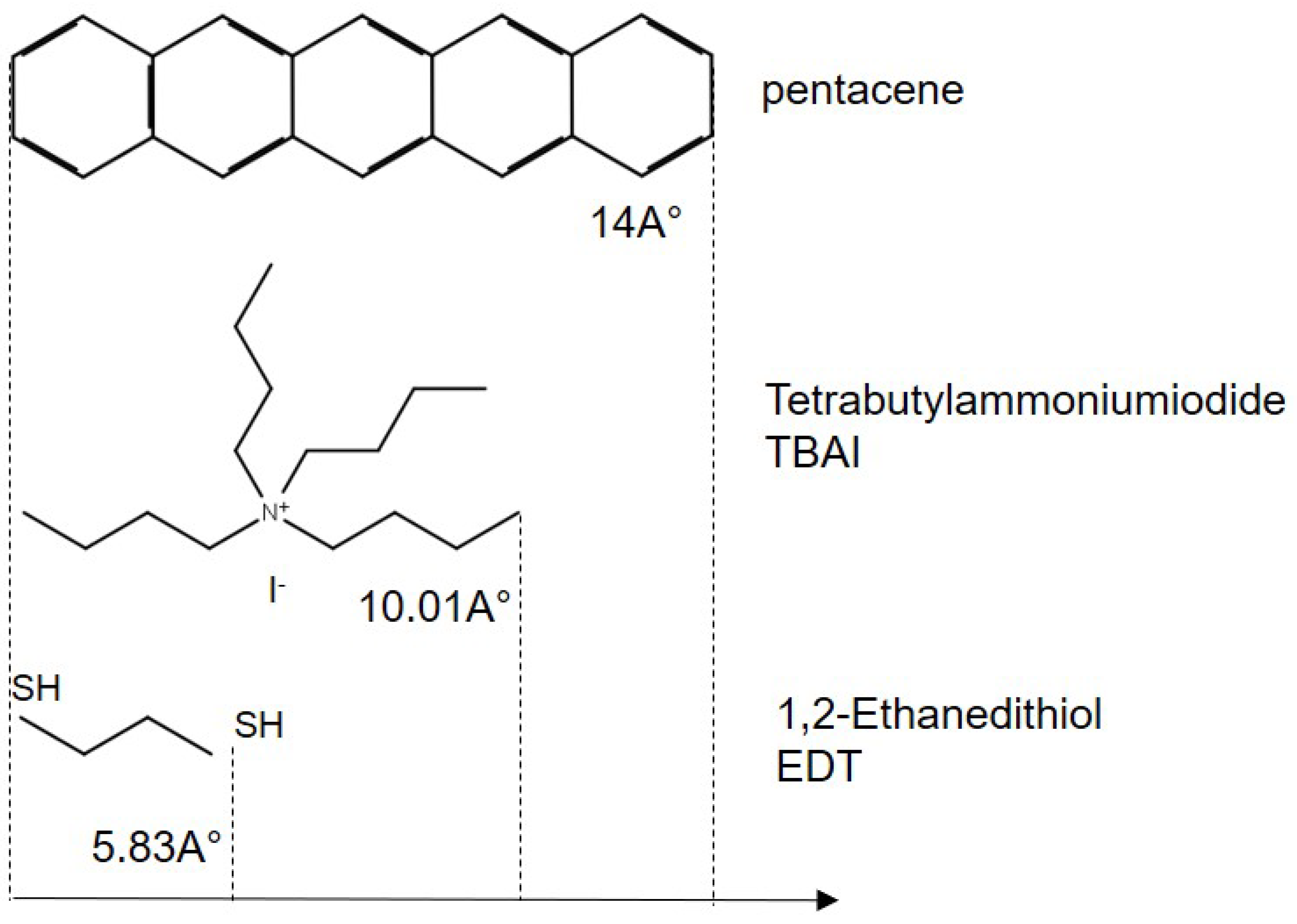
20]. In this work, OA is replaced by two different types of ligands (EDT and TBAI),
Figure 1. EDT ligand in solution and TBAI ligand as powder were purchased from Sigma Aldrich and diluted in acetonitrile and methanol, respectively. Ligand exchange was performed by spin coating one of the ligands EDT, TBAI and PbS-NCs layers sequentially to exchange the olic acid by the ligand. Each ligand exchange step is followed by a washing process. This process is repeated until we get the required thickness. To avoid air exposure, samples were prepared in a nitrogen environment inside a glove box as oxygen and hydroxyl (
) were observed attached to the PbS-NCs’ surface of (111) facets by Fourier-transform infrared spectroscopy as in the reference [
21]. Pentacene from TCI supplier, Bathocuproine (BCP) from Sigma Aldrich, poly(3,4-ethylenedioxythiophene) polystyrene sulfonate (Clevios™ P AI4083 PEDOT:PSS) from Heraeus Clevios GmbHwere used. The work functions of PEDOT:PSS (4.9 eV) [
22]were measured with UPS, see supporting information S 2.
2.2. Device Preparation
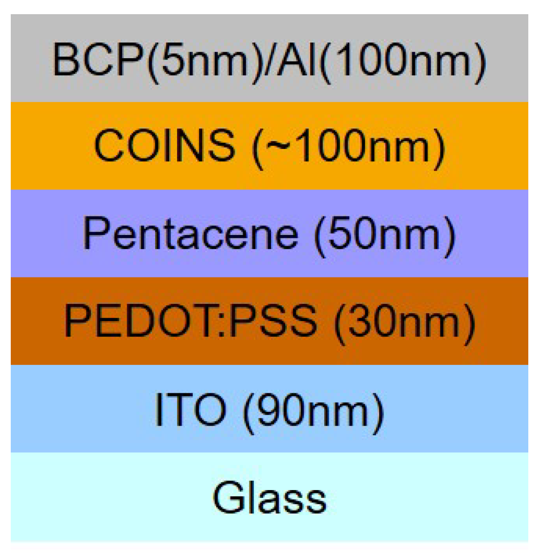
A stack configuration for our devices has been performed in the experiments which is illustrated in
Figure 2; (ITO/PEDOT:PSS/pentacene/COINs/BCP/Al).
Substrates were cleaned for 15 minutes in an ultrasonic bath with acetone and isopropanol. Plasma treatment followed the cleaning process. PEDOT:PSS was spin-coated from aqueous dispersion and subsequently dried at 100 °C for 1 hour. Organics and metals were all evaporated in ultra high vacuum ( mbar).
2.3. Experimental Methods
Transmission electron microscopy (TEM) was performed on a JEOL Neoarm F200 with a cold field-emission gun (Cold FEG) using carbon-coated copper grids (type S160-3) from Plano (Germany), operated at 200 keV electron beam energy under vacuum. Samples were scanned under ambient atmosphere with the scanasyst mode of atomic force microscopy (AFM) from Bruker company. Ultraviolet Photoelectron Spectroscopy (UPS) was performed in ultra high vacuum (UHV) using He I radiation (21.22 eV) from a gas discharge lamp and the radiation was attenuated by passing through an aluminum foil (350 nm) before reaching the sample to minimize sample damage. Survey data was collected from X-ray photoelectron spectroscopy (XPS) using a non-monochromatic MgK
radiation (1.2536 keV). A pass energy of 2.0 eV for UPS, 20 eV and 50 eV for high-resolution and survey XPS scans were used. By measuring the Fermi edge of a clean Au surface, it was possible to determine the energy resolution and energy scale calibration. A bias of (-10V) was applied to measure the secondary electron cut-off (SECO). Photodiodes were measured with Keithley 236 SMU in the dark and under one sun simulated AM1.5G, 100 mW/cm
2 illumination with a Xe lamp (Oriel 300 W with AM1.5G filters) integrated in a glove box system with nitrogen atmosphere. Current-voltage characteristics were measured from -1.5 V to 1.5 V in 0.05 V steps [
23].
IPCE (incident photon-to-current efficiency) measurements were carried out under vacuum in a cryostat using a monochromatic illumination from an Omni-300 Monochromator/Spectrograph, Zolix Instruments and lock-in amplifier. The thicknesses of the films, refractive index (n) and excitintion coefficient (k) were obtained from Ellipsometry (SE-850 and Spectraray/3 from SENTECH GmbH).
3. Results
This section summarizes the findings made about a comparison between the optoelectrical properties of two different ligands. Structure and morphology of the films were investigated using TEM and AFM. Also, the electronic structure of the energy levels were studied using ultraviolet photoelectron spectroscopy. Moreover, the electrical and optical properties were measured using different set-ups like sun-simulator, PAIOS and incident photon to current efficiency (IPCE).
3.1. Transmission Electron Microscope (TEM)
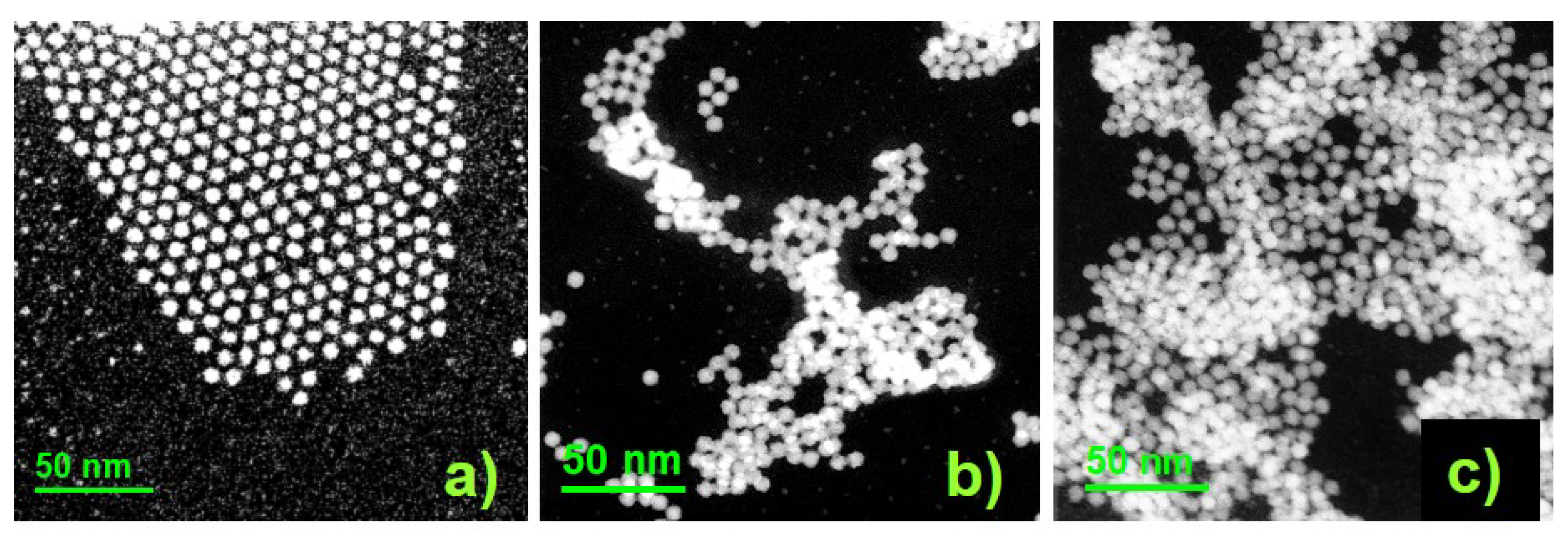
Images of PbS-NCs with different ligands under a conventional scanning transmission electron microscope STEM are shown in
Figure 3 (a, b and c) and S 3-S 5. The STEM image in Figure S 3 and the corresponding histogram of native OA-capped PbS-NCs in Figure S 4 reveal large size (6.1+/-0.9 nm) PbS-NCs capped with oleic acid (OA). Hexagonal order for these nanoparticles is observed in the first monolayer. This superlattice is initiated from the weak bond of oleic acid with NCs and prevents them from aggregation. The interparticle distances among the nanoparticles can be measured either directly from the real images or by tracing a cross section for the live profile of several particles and then calculating the distance by dividing the number of the NCs and subtracting the diameter of PbS-NC. There is another possibility to obtain the average distance from the fast Fourier transform (FFT) of a certain area of STEM images, as seen in the supporting information (Figures S 3-S 5, Table S 1). We selected the monolayer for FFT and excluded the clusters of PbS-NCs. Several atomic lattice planes of PbS crystal from the atomic resolution scale of TEM images were distinguished such as (200), (111) and more. There were other lattice planes detected from the diffraction pattern of FFT which are illustrated in the supporting file, Figures (S 67-S 9) and Table S 2.
The length of an EDT molecule is 0.58 nm according to our simulation with Schrödinger’s Materials Science Suite; however, the average distance is hardly measurable in the STEM image as the PbS-NCs have almost merged in both cases of EDT and TBAI. NCs in
Figures 3b and c have the tendency to be accumulated in different units with dimers, trimers and more in tetragonal alignment. These units grow in three dimensional shapes with barren areas among them. This initial seed-layer of PbS-NCs and ligand form the base coverage of the consequential layers. The NCs with EDT and TBAI in
Figure 3b and c seem to be merged. This behavior suggests a strong interaction between the PbS-NCs and the bifunctional thiols EDT ligands. The EDT here play the role of a double-sided linker between each two adjacent NCs by replacing two of its hydrogen atoms at both terminals. A similar narrative has been observed for TBAI Figure (3c) which has a salt-like structure. The reaction of EDT and TBAI has been examined thoroughly in the literature [
17,
24,
25,
26]. The
I−1
anions substitute divalent
S−2 anions within PbS-QDs and bind to the NCs’ surface to repel oxidative attack [
24]. Therefore, the coverage of the NCs and ligands depends mainly on the interaction between PbS-NCs and type of ligand.
TEM images in Figures(S 6-S 9) of the supporting information reveal that EDT and TBAI ligands have no preferable plane to react with PbS-NCs as all set planes are facing the projection of the TEM camera.
3.2. Atomic Force Microscope (AFM)
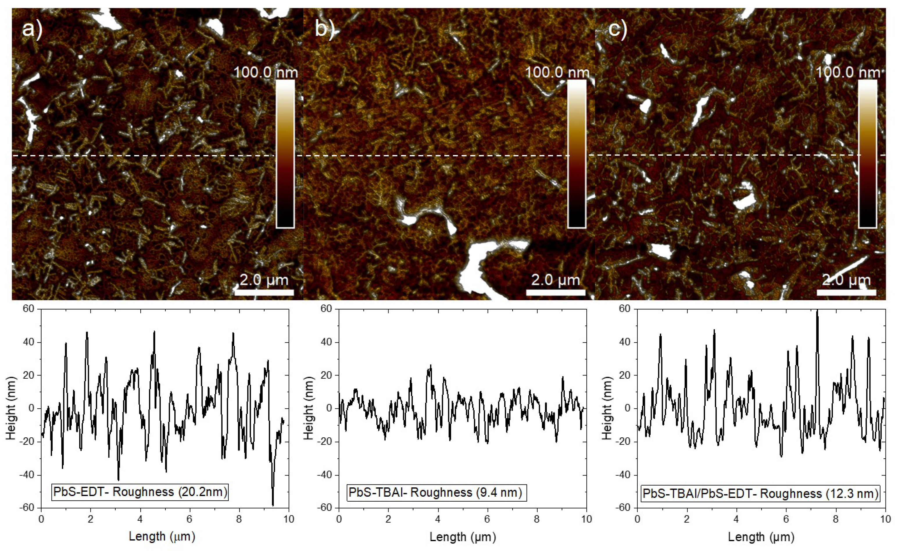
AFM images of PbS-NCs with ligands on ITO/PEDOT:PSS/pen substrates are shown in
Figure 4. Average thicknesses and roughness are listed in
Table 1 for disparate COINs.
Figure 4 (a - c) reveals a complete COINs coverage. Nonetheless, the roughness and grain sizes are different as given in
Table 1. These COINs are the outgrowth of the early monolayers which have been demonstrated in STEM images. Due to three dimensional aggregation, they have obtained a fiber-like structure on pentacene/PEDOT:PSS with high roughness. If we compare the effect of ligand types on roughness, EDT has a higher roughness than TBAI.
3.3. Ultraviolet Photoelectron Spectroscopy (UPS)
Ligands were classified according to their electrons donation to
cations. Ligands which donate 1 electron are called X-type e.g. iodide, carboxylates, thiolates [
27]. The neutrality and Fermi level position with respect to LUMO or HOMO level depends on the charge balance and thermodynamic stability of quantum dots (QDs) and ligands together. Fermi level determines the semiconductor type of the final PbS-ligand films. Therefore, it was necessary to measure valence level and work function of COIN films by photoelectron spectroscopy (UPS).
UPS was measured for multi-layer films deposited on ITO substrates to determine the energy levels (valence level and work function). Chemical composition of the films were measured by XPS to assure a full layer coverage to the ITO. To better understand the behavior of our photodiodes, data from UPS and XPS were measured, analyzed and correlated to the device characteristics. UPS and XPS results are illustrated in detail in the supporting file, Figure S 2. The low-binding energy onset of the occupied density of states represents the valence level (VL) with respect to the Fermi level, while the secondary electron cut-off (SECO) determines the work function at high binding energy.
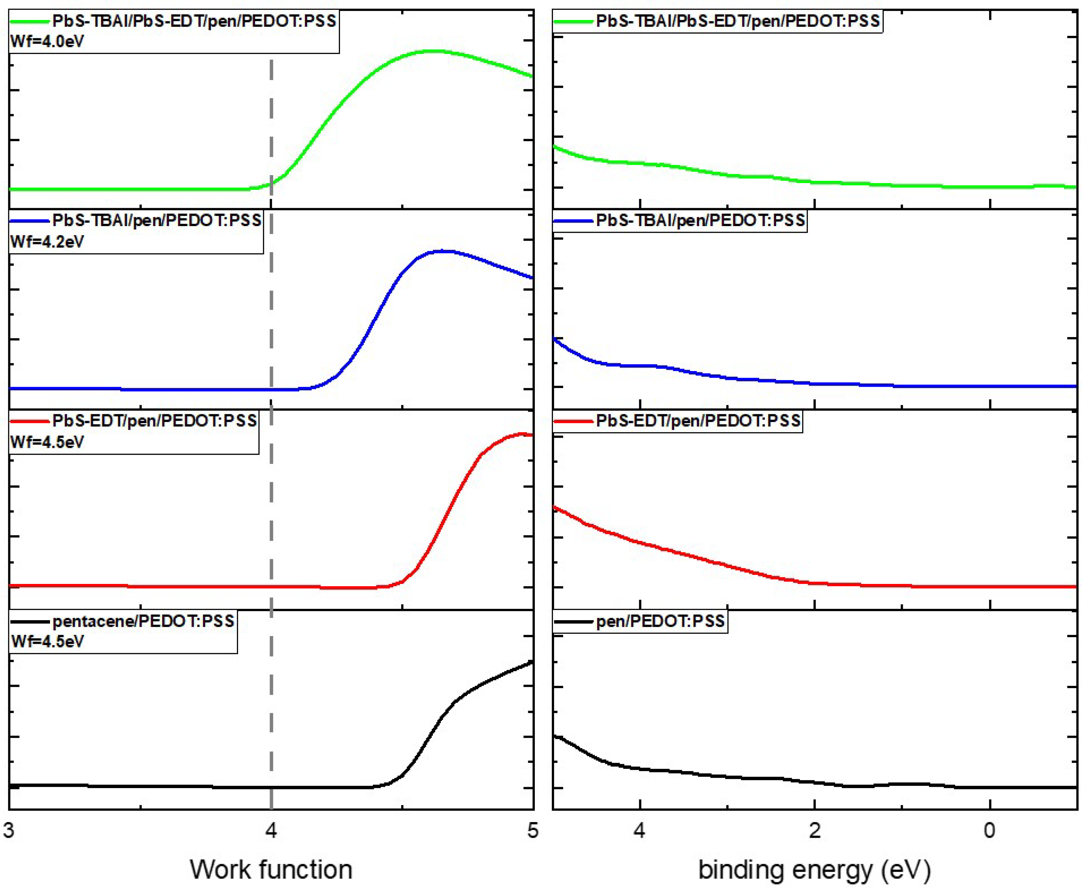
Figure 5 show the secondary electron cut-off of the different layers on PEDOT:PSS with the energy scale converted to the resulting work function.
The low binding energy onset with respect to the Fermi level corresponds to the
level of PbS-NCs. This value is obtained from an extrapolation of the curve to the instrumental background. The work function for the same type of PEDOT:PSS was measured before [
22]. When we deposit COINs on PEDOT:PSS, the work function is changed from (4.9eV) to minimum value of (4.0eV) in case of hetrostructure COINs/pentacene,
Figure 5. The difference in the work functions of PbS-EDT and PbS-TBAI attributes to the difference between the Pb-halide anion and the Pb-thiol interactions, which give rise to different surface dipole moments as studied elsewhere [
14].
XPS measurements which are shown in Figure S 2 in the supporting information, have very strong signals to Pb and S atoms and there were no residual Indium signals detected for all samples. The energy diagram of highest occupied energy levels (HOMO) and the lowest unoccupied energy levels (LUMO) of different layers are assigned in
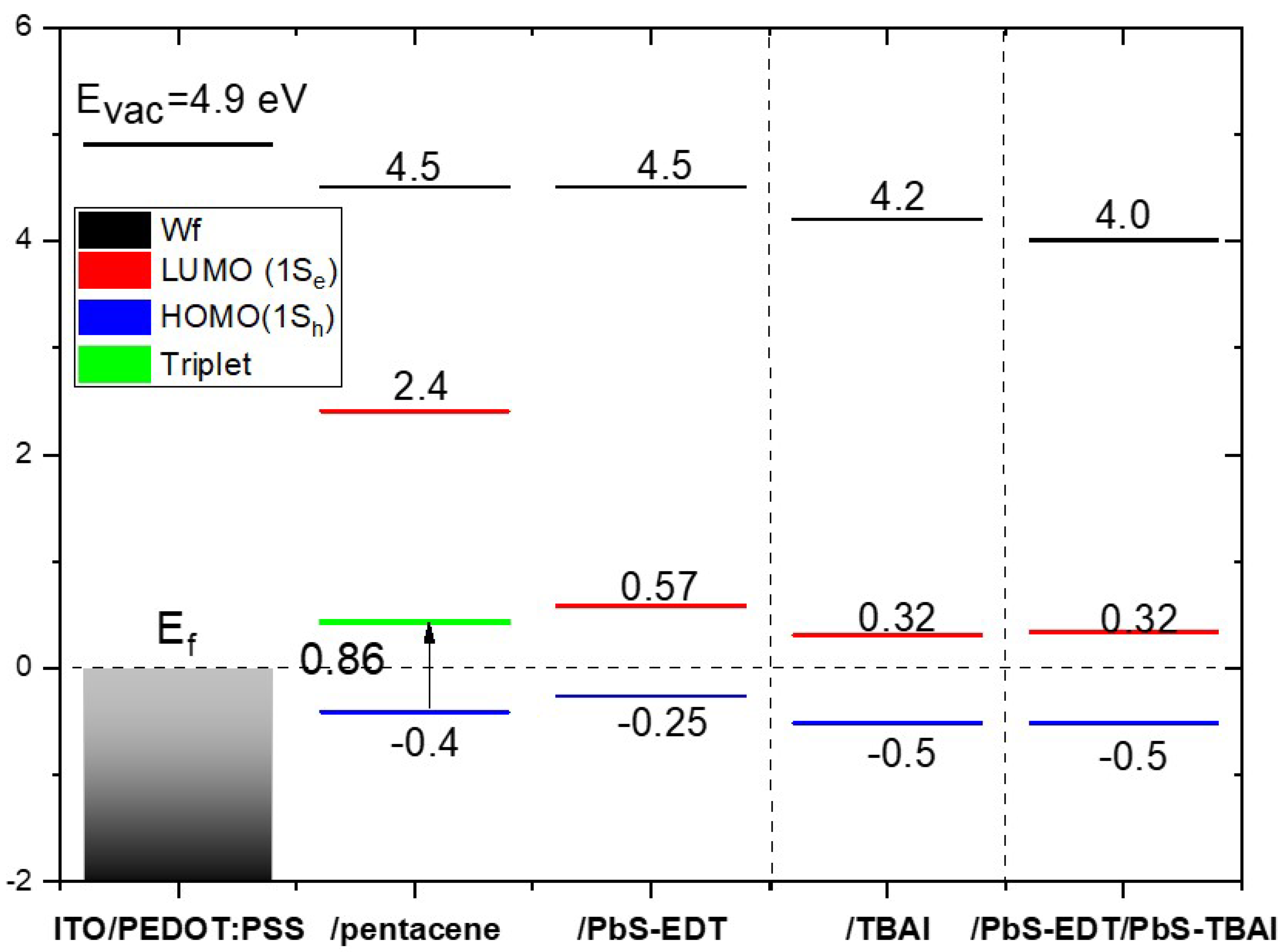
Figure 6.
The optical energy gap of the NCs is around (0.78eV). The transport energy gap of the coupled organic-inorganic materials depends strongly on the dielectric constant of the chosen ligands and the solvents [
14,
28]. Therefore, the effective dielectric constants of COINs with variant ligands were calculated (supporting information, Table S 3) according to the Maxwell-Garnett effective medium theory [
29].
The volume factors were found from TEM images and they have been found to be around 0.74 for PbS-EDT and 0.7 for PbS-TBAI (supporting information). The optical band gap of pentacene has been calculated from the onset value of the measured absorption spectrum in the supporting file at (1.8eV).
3.4. Electrical Characteristics
Inorganic–organic photovoltaic devices with a structure of organic pentacene and PbS-NCs have been electrically characterized in this section. The current flow in the organic-inorganic semiconductor diode is illustrated in
Figure 7. An ohmic injection contact with a proper electrode was chosen for the stack,
Figure 2. In any diode, there are two regions: diffusion and drift current region which arise from the difference in the carrier concentration and a drift of these carriers, resulting in a space charge region (SCLC). The
is then equal to the barrier height. At low positive applied voltage, the diffusion current is dominant over the drift current. The classical Shockley diode equation describes the current density versus applied voltage for the diode[
30]:
is the saturation current,
is the ideal factor, K is Boltzmann constant and T is the temperature.
At high positive voltage, larger than the built-in voltage, the electric field becomes positive. Electrons and holes are injected and they would be dominant by drift current. The current becomes limited by the uncompensated charges of the injected carriers, leading to a space- charge-limited current that can be described by Mott-Gurney formula[
31]:
is the effective mobility, d is the thickness. The current density versus voltage under illumination is given by [
32]:
The series resistance lowers the effective voltage at the junction by and parallel shunt resistance .
Parameters like the short-circuit current (
), open-circuit voltage (
), which are listed in
Table 2, were extracted from the current density-voltage characteristics in
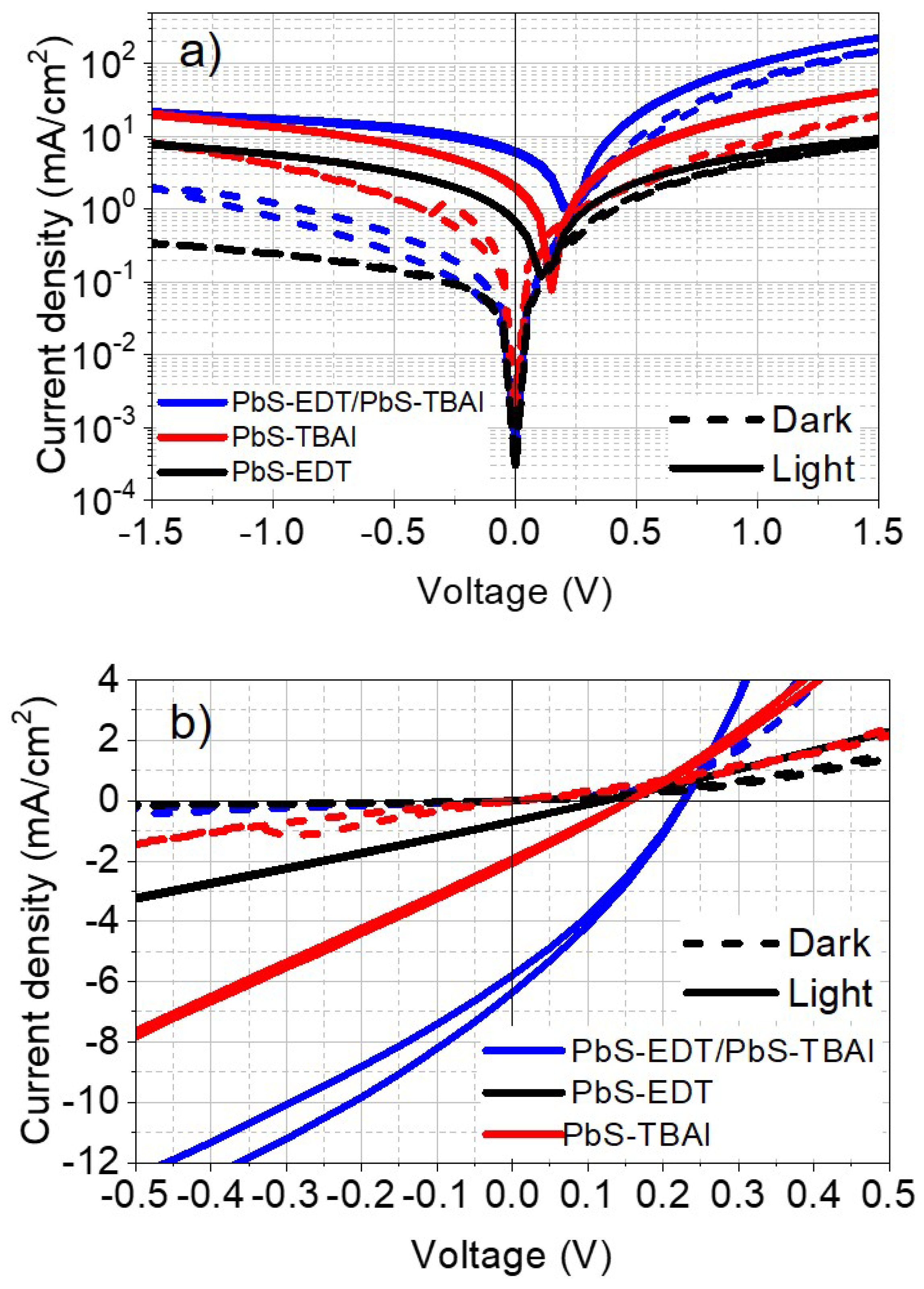
Figure 7. The parasitic resistances like the series resistance and the shunt resistance play a main role to identify the measured devices as diodes and how close are they to the ideal. It is clear from the current density-voltage characteristics in
Figure 7 that the diodes with EDT have the lowest leakage current. On the other hand, samples with TBAI or heterostructure ligands have a remarkable leakage current. This leakage current can be mainly attributed to the morphology of the COINs. Higher short circuit current density
, open circuit voltages, filling factor and efficiency were obtained from the double heterosubstructure stack as shown in
Table 2. The calculated onset voltages from the energy level diagrams in
Figure 5 of the fabricated devices are given in
Table 3.
The difference between the calculated and the real values would correspond to the losses in the inter-layers. The quasi Fermi level is iso-energetic when the solar cell is not illuminated. The Fermi level is splitting into two quasi-Fermi states
and
because of the charge carriers under illumination [
33]. Therefore, the energetic difference between the HOMO-LUMO level of adjacent heterostructure layers and the
would give the losses. These losses originate from different reasons such as an energetic disorder [
33]. When there is no flowing current, the measured voltage will represent the open circuit voltage (
)[
33,
34]: e
=
-
=
-
-
.
Figure 7.
Current-voltage characteristics for logarithmic and linear scale for the samples.
Figure 7.
Current-voltage characteristics for logarithmic and linear scale for the samples.
3.5. Incident Photon to Current Efficiency (IPCE)
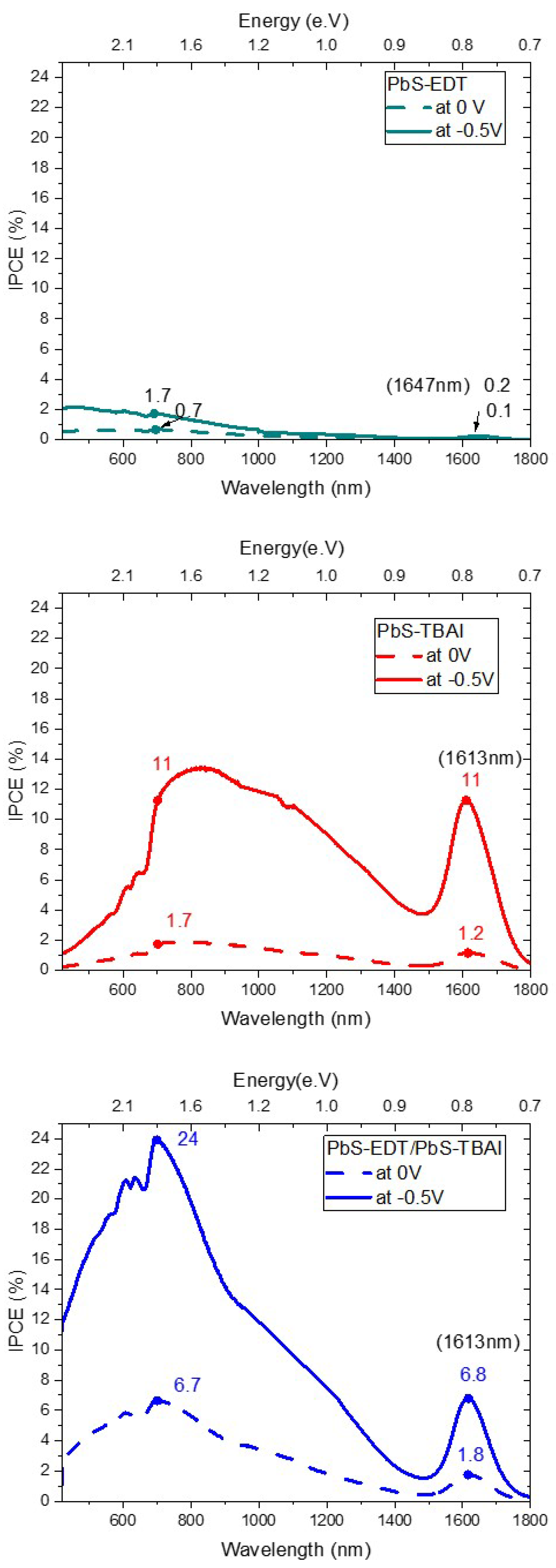
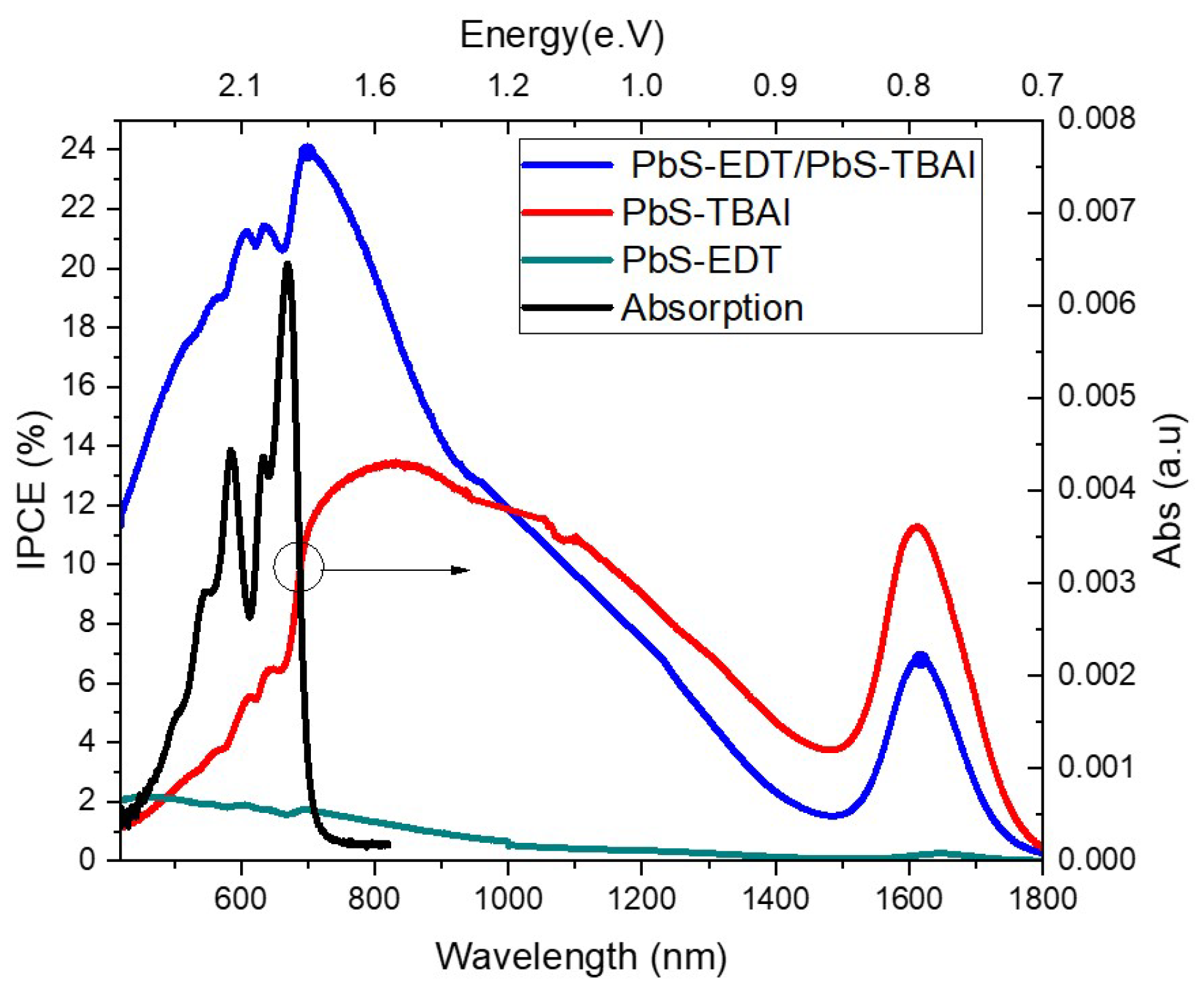
Figure 8 reveals the different current response of the samples to the applied photons from the monochromator of the IPCE setup. The main absorption peak of Pb NCs is around 1613nm. Samples with higher short circuits like the double type of ligands heterostructure obtained higher current signal at IPCE measurement. However, the increment of the IPCE is more than the double IPCE signal obtained from the single type devices with EDT or TBAI alone. EDT is a non-conjugated molecule, therefore, the broadened peaks in the range of (900-1300 nm) belong to the higher excitation states of PbS-NCs. These peaks are observed also in the IPCE spectra. A red shift at the solid phase of the PbS-NCs is observed in our sample upon the excitonic absorption peaks at (1613nm) of the NCs in solution. Another small red displace of around 34nm with EDT ligand samples was also detected. A similar shift has been reported by our group [
10] while this shift disappeared in the heterostructure samples with TBAI. Researchers who studied the effect of different ligands like EDT on the photoluminescence of PbS-QDs attributed this shift to several reasons [
35]. These reasons are summarized as several points like: i) strong coupling among the NCs, ii) dipole-dipole interaction and its effect on the line shape of the emission or iii) quantum confinement effect because of different delocalized wave functions of different ligands. However, they mainly attributed the reason to the strong coupling between the NCs and the ligands. Our results would contradict their conclusion. If the strong coupling would effect the red shift, we would have to see this displacement more at samples which have TBAI because NCs are agglomerated as we have observed in TEM and AFM images. The quantum confinement due to the ligand effect is more likely the reason for this shift. The dielectric constant variation is one piece of evidence that supports the hypothesis of quantum confinement.
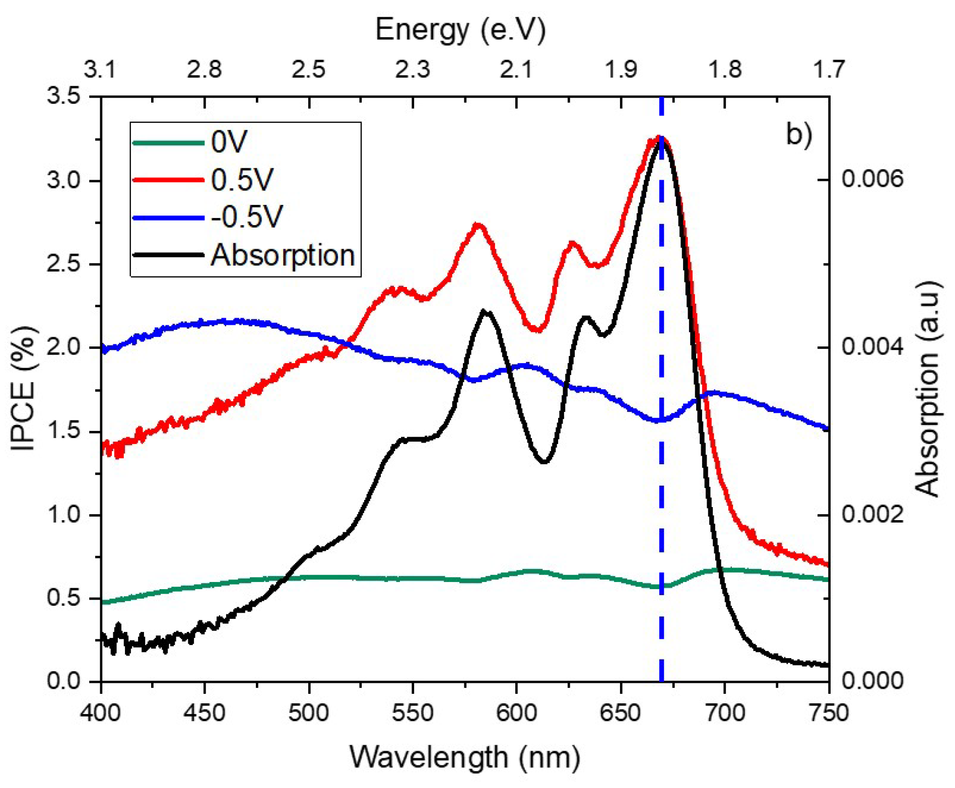
Because BCP have a large optical band gap of (3.5 eV), they play a role of a transparent layer for the visible light [
36,
37]. This leads to light reflection at the aluminum and gold surface. The interference of the incident and reflected wavelength and the extra absorption of the light would manifest inverted peaks which are outcropped in the visible range of IPCE signals. This effect is attributed to the spatial collection efficiency because of Fabry-Pe’rot effect and polydispersity of density of states [
38].
A finger print of the conjugated molecule like pentacene appears as vibrionic peaks in the visible range. The vibrionic spectra of pentacene are not clearly observable in the curves of
Figure 8 when no applied voltage was applied because the absorption of COINs is higher in the visible range as well as the infrared. The signal became more recognizable when we applied reverse bias because the latter improves the carrier charge separation. In
Figure 9 and
Figure 10, we observed inverted peaks in correspondence to the position of pentacene vibrionic peaks. We can attribute these upside down peaks to the re-absorption of the reflected photons at the metal contact and interference effect. However, this observation adds another complexity to be understood when we applied a positive bias. Applying a positive voltage maintains the vibronic peaks of pentacene without a spectral shift,
Figure 10. This led us to other conclusions, whether optical dielectric constant is effected by the charge accumulation at the interfaces of the films or applying voltage would have an effect on the molecular polarization [
39,
40].
4. Discussions
From the review above, key findings emerge: Disordered films are formed from the coupled PbS and EDT, TBAI ligands as they appear in the TEM and AFM images. The irregular distribution of PbS-ligands is attributed to the short interparticle distances and formation of many voids and agglomeration on the monolayer level. This finding demonstrated that the morphology of the films plays a fundamental role in the optoelectronic properties of the devices.
In this section, we will discuss the difference between the single type of ligands and the double type of ligands (EDT and TBAI) in a heterostructure diode of pentacene/PbS-COINs. According to literature [
14], PbS-TBAI has a LUMO level lying below the PbS-EDT. This reference [
14] was the inspiration for us to apply a double type of ligand heterojunction in our research. Before we start our discussion regarding the double type ligands heterostructure, we address the difference in electronic energy levels and electrical characterization between these two different COINs of PbS-EDT and PbS-TBAI separately. The diagram in
Figure 5 shows the difference of PbS-EDT and PbS-TBAI energy levels on pentacene/PEDOT:PSS. Quasi Fermi level of COINs on ITO/PEDOT:PSS/pentacene is shifted down to align with the pentacene Fermi level. Here, the Fermi level sets at zero and is considered to be the reference of HOMO-LUMO levels for all the layers. Another shift can be observed also at the HOMO and LUMO levels. In case of PbS-EDT on pentacene, the HOMO level is slightly above the HOMO level of pentacene alone while the HOMO of PbS-TBAI and PbS-EDT/PbS-TBAI are lower than the HOMO of pentacene. HOMO position would block the holes and that explains the drawback in the performance of PbS-EDT. As we have seen in
Figure 5, the optical energy under the LUMO level of PbS-EDT is relatively higher than the triplet state of pentacene. That indicates that transferring the photo generated exciton from pentacene to the optical energy of COINs is impractical. Yet this is possible in the case of PbS-TBAI where the optical energy level is much closer to the triplet state of pentacene. The difference in the vacuum level in terms of the work function represents the dipole effect at the interface between pentacene and the COINs. The exciton binding energies were calculated for EDT and TBAI. They have a difference in value as illustrated in Table S3 in the supporting file [
41]. Mainly, the exciton energy level value and LUMO level position depend on the surrounding dielectric constant of COINs and particle size. When we recall the images of TEM, PbS-TBAI revealed better substance coverage than PbS-EDT. However, TBAI COINs shows worse diode behavior and it has a short-circuit tendency (
Figure 7). The EDT sample has better diode characteristics with a clear injection region. The charge separation at the reverse bias in the case of EDT also is eminent between the dark current and photocurrent. On the other hand, both ligands in
Figure 7 show diode characteristics and the difference between the dark and photocurrent at the reverse bias is relatively significant. To improve the energy levels adaption and transfer of excitons, a double type of ligands heterostructure was employed in this research.
Figure 7 demonstrates the difference between the single types of photodiodes and the stack of combined heterostructure COINs (PbS-EDT/PbS-TBAI). The current versus voltage graphs show a better and clear injection region in the EDT and the stack of double ligands heterostructure sample. These results correspond to the energy level diagrams from UPS in
Figure 5. An improvement of current injection is discerned in the double ligands heterostructure photodiode. This enhancement results from the modification of the energy level positions of HOMO-LUMO levels of PbS-EDT/PbS-TBAI relative to the pentacene levels at the interface which allows better injection for both electron and holes. This suggests a better photo detection and exciton separation.
In general, the electrons are blocked to be transferred from the COINs to pentacene in the dark current as they appear in
Figure 7. Oppositely, the photo carriers exhibit an inverse direction. Therefore, for the heterostrcuture device in
Figure 7, the photo generated electron-hole pairs are able to be transferred inside these layers. The low short circuit current for EDT single type ligands indicates that triplet excitons are lost which are initiated from singlet fission in pentacene molecules on their way to the optical energy state in COINs. The exciton losses can be attributed not only to the energy level alignment but to the distance between pentacene molecules and COINs as well. Obviously, only the molecules and NCs which are at the interface would exchange their energy and the rest of excitons can recombine meanwhile. We also observed that this result can be affected by many factors like EDT concentration and layer thickness. In general, TBAI single type photodiode and the double heterostructure sample show leakage current which suggests low shunt resistance in many samples and this is an indication of high trap concentrations. The onset voltage difference between the donor-acceptor layers are listed in
Table 3. It is obvious that using TBAI ligand lowers the onset voltage which suggests increasing the conductivity and the current of the sample. TBAI can lower the work function and the ionization potential by introducing a dipole at the surface while EDT layers show no change of the work function. An improvement is observed in the photocurrent of the double heterostructure. The reason can be attributed to the thickness of the heterostructure, which is double the thickness of the single type of COINs. Another reason can be attributed to the variation of work function and dipole effect and hence this leads to a change of built in potential and the internal electrical field which can have an effect on the charge separation in the diffused interfaces among the heterostructure layers. The improvement at the heterostructure samples were observed mainly in the short circuit current and the IPCE signal. The vibronic peaks of the pentacene can be observed significantly at applied reverse voltage. The applied voltage can separate the charge carriers and improve the external quantum efficiency.
The increment of the IPCE signal at reverse voltage upon no applied voltage are found to be 6.5 and 9.2 times in case of TBAI single type ligand sample at the visible and infrared ranges, respectively. On the other hand, the increment is much lower in case of EDT single ligand type sample and the heterostructure sample. In case of EDT, it is only double in both ranges while in case of the heterostructure is around four times. We can attribute this to the alignment of the HOMO level of the PbS-EDT above the HOMO level of pentacene which blocks the holes.
5. Conclusion
Our results casts light on a new type of organic-inorganic photodiodes. In conclusion, the implementation of a singlet fission layer like pentacene with a double type ligands heterostructure improves the photocurrent, opet circuit voltage filling factor and the efficiency of a photodiode in comparison to the single type of ligands in a coupled organic-inorganic nanostructure films. The enhancement of the short-circuit current is only the first stepping stone which provides evidence for transferring the photoelectrons from the triplet state of pentacene to the PbS-NCs. Furthermore, charge separation and the difference between the photocurrent and dark conductivity current need to be ameliorated. Moreover, replacing EDT and TBAI by other linker molecules may significantly improve the photodiode performance. Our findings add to a growing corpus of research showing that several parameters can have an effect on the photodiode performance like; ligand type, ligand concentration, particle size, COINs’ thickness, diode structure (stack) and recombination. From the UPS measurement, we can conclude that the electronic and optical properties of the different COINs are explained by an effective-medium theory based on their binding and the structural arrangements.
According to our results, using TBAI instead of the EDT ligand improves the photodiode parameters: Increase the electron transfer from the triplet state of pentacene to the COINs by manipulating the position of energy levels of COINs and decrease the work function according the UPS results. Decreasing the work function leads to better charge carrier injection by decreasing the barrier height. This improvement was observed furthermore for the heterostructure samples by improving the short circuit current and the IPCE signals.
Supplementary Materials
The following supporting information can be downloaded at the website of this paper posted on
Preprints.org.
The following supporting material is available:
Absorption
Energy Levels, UPS and XPS
Transmission Electron Microscope
Effective Dielectric Constant
Ligand Concentrations
Acknowledgments
This work was funded by the German Research Foundation (DFG) under Project No. BR 1728/18-1. A.M. has received funding by the DFG under Project No. BR 182087777 - SFB
951
References
- Scheele, M.; Hanifi, D.; Zherebetskyy, D.; Chourou, S.T.; Axnanda, S.; Rancatore, B.J.; Thorkelsson, K.; Xu, T.; Liu, Z.; Wang, L.W.; others. PbS nanoparticles capped with tetrathiafulvalenetetracarboxylate: utilizing energy level alignment for efficient carrier transport. ACS nano 2014, 8, 2532–2540. [Google Scholar] [CrossRef]
- Ehrler, B.; Wilson, M.W.B.; Rao, A.; Friend, R.H.; Greenham, N.C. Singlet exciton fission-sensitized infrared quantum dot solar cells. Nano letters 2012, 12, 1053–1057. [Google Scholar] [CrossRef] [PubMed]
- Smith, M.B.; Michl, J. Singlet fission. Chemical reviews 2010, 110, 6891–6936. [Google Scholar] [CrossRef]
- Papa, C.M.; Garakyaraghi, S.; Granger, D.B.; Anthony, J.E.; Castellano, F.N. TIPS-pentacene triplet exciton generation on PbS quantum dots results from indirect sensitization. Chemical science 2020, 11, 5690–5696. [Google Scholar] [CrossRef]
- Garakyaraghi, S.; Mongin, C.; Granger, D.B.; Anthony, J.E.; Castellano, F.N. Delayed molecular triplet generation from energized lead sulfide quantum dots. The journal of physical chemistry letters 2017, 8, 1458–1463. [Google Scholar] [CrossRef]
- Pun, A.B.; Asadpoordarvish, A.; Kumarasamy, E.; Tayebjee, M.J.Y.; Niesner, D.; McCamey, D.R.; Sanders, S.N.; Campos, L.M.; Sfeir, M.Y. Ultra-fast intramolecular singlet fission to persistent multiexcitons by molecular design. Nature chemistry 2019, 11, 821–828. [Google Scholar] [CrossRef]
- Davis, N.J.L.K.; Allardice, J.R.; Xiao, J.; Petty, A.J.; Greenham, N.C.; Anthony, J.E.; Rao, A. Singlet fission and triplet transfer to PbS quantum dots in TIPS-tetracene carboxylic acid ligands. The journal of physical chemistry letters 2018, 9, 1454–1460. [Google Scholar] [CrossRef]
- Hu, L.; Mandelis, A.; Yang, Z.; Guo, X.; Lan, X.; Liu, M.; Walters, G.; Melnikov, A.; Sargent, E.H. Temperature-and ligand-dependent carrier transport dynamics in photovoltaic PbS colloidal quantum dot thin films using diffusion-wave methods. Solar Energy Materials and Solar Cells 2017, 164, 135–145. [Google Scholar] [CrossRef]
- Liu, Y.; Gibbs, M.; Puthussery, J.; Gaik, S.; Ihly, R.; W. Hillhouse, H.; Law, M. Dependence of Carrier Mobility on Nanocrystal Size and Ligand Length in PbSe Nanocrystal Solids. Nano Lett 2010, 10, 1960–1969. [Google Scholar] [CrossRef] [PubMed]
- Scheele, M.; Brütting, W.; Schreiber, F. Coupled organic-inorganic nanostructures (COIN). Physical Chemistry Chemical Physics 2015, 17, 97–111. [Google Scholar] [CrossRef]
- Erslev, P.T.; Chen, H.Y.; Gao, J.; Beard, M.C.; Frank, A.J.; van de Lagemaat, J.; Johnson, J.C.; Luther, J.M. Sharp exponential band tails in highly disordered lead sulfide quantum dot arrays. Physical Review B 2012, 86, 155313. [Google Scholar] [CrossRef]
- Moreels, I.; Lambert, K.; Smeets, D.; De Muynck, D.; Nollet, T.; Martins, J.C.; Vanhaecke, F.; Vantomme, A.; Delerue, C.; Allan, G.; others. Size-Dependent Optical Properties of Colloidal PbS Quantum Dots. ACS Nano 2009, 3, 3023–3030. [Google Scholar] [CrossRef]
- Weidman, M.C.; Beck, M.E.; Hoffman, R.S.; Prins, F.; Tisdale, W.A. Monodisperse, Air-Stable PbS Nanocrystals via Precursor Stoichiometry Control. ACS nano 2014, 8, 6363–6371. [Google Scholar] [CrossRef] [PubMed]
- Brown, P.; Kim, D.; Lunt, R.; Bawendi, M.; Grossman, J.; Bulovic, V. Energy level modification in lead sulfide quantum dot photovoltaics through ligand exchange. APS 2014, 2014, L24–002. [Google Scholar] [CrossRef]
- Ganesan, A.A.; Houtepen, A.J.; Crisp, R.W. Quantum dot solar cells: Small beginnings have large impacts. Applied Sciences 2018, 8, 1867. [Google Scholar] [CrossRef]
- Tabachnyk, M.; Ehrler, B.; Gélinas, S.; Böhm, M.L.; Walker, B.J.; Musselman, K.P.; Greenham, N.C.; Friend, R.H.; Rao, A. Resonant energy transfer of triplet excitons from pentacene to PbSe nanocrystals. Nature materials 2014, 13, 1033–1038. [Google Scholar] [CrossRef]
- Maiti, S.; André, A.; Banerjee, R.; Hagenlocher, J.; Konovalov, O.; Schreiber, F.; Scheele, M. Monitoring self-assembly and ligand exchange of PbS nanocrystal superlattices at the liquid/air interface in real time. The journal of physical chemistry letters 2018, 9, 739–744. [Google Scholar] [CrossRef]
- Choi, H.; Ko, J.H.; Kim, Y.H.; Jeong, S. Steric-hindrance-driven shape transition in PbS quantum dots: understanding size-dependent stability. Journal of the American Chemical Society 2013, 135, 5278–5281. [Google Scholar] [CrossRef]
- Beygi, H.; Sajjadi, S.A.; Babakhani, A.; Young, J.F.; van Veggel, F.C.J.M. Surface chemistry of as-synthesized and air-oxidized PbS quantum dots. Applied Surface Science 2018, 457, 1–10. [Google Scholar] [CrossRef]
- Heuer-Jungemann, A.; Feliu, N.; Bakaimi, I.; Hamaly, M.; Alkilany, A.; Chakraborty, I.; Masood, A.; Casula, M.F.; Kostopoulou, A.; Oh, E.; others. The role of ligands in the chemical synthesis and applications of inorganic nanoparticles. Chemical reviews 2019, 119, 4819–4880. [Google Scholar] [CrossRef]
- Tom, A.E.; Thomas, A.; Ison, V.V. Novel post-synthesis purification strat egies and the ligand exchange processes in simplifying the fabrication of PbS quantum dot solar cells. RSC Advances 2020, 10, 30707–30715. [Google Scholar] [CrossRef]
- Wagner, J.; Gruber, M.; Hinderhofer, A.; Wilke, A.; Bröker, B.; Frisch, J.; Amsalem, P.; Vollmer, A.; Opitz, A.; Koch, N.; others. High fill factor and open circuit voltage in organic photovoltaic cells with diindenoperylene as donor material. Advanced Functional Materials 2010, 20, 4295–4303. [Google Scholar] [CrossRef]
- Brütting, W.; Riel, H.; Beierlein, T.; Riess, W. Influence of trapped and interfacial charges in organic multilayer light-emitting devices. Journal of Applied Physics 2001, 89, 1704–1712. [Google Scholar] [CrossRef]
- Gao, W.; Zhai, G.; Zhang, C.; Shao, Z.; Zheng, L.; Zhang, Y.; Yang, Y.; Li, X.; Liu, X.; Xu, B. Towards understanding the initial performance improvement of PbS quantum dot solar cells upon short-term air exposure. RSC advances 2018, 8, 15149–15157. [Google Scholar] [CrossRef]
- Sengupta, S.; Loutaty, R.; Petel, K.; Levin, E.; Lemcoff, N.G.; Golan, Y. The effect of short chain thiol ligand additives on chemical bath deposition of lead sulphide thin films: the unique behaviour of 1, 2-ethanedithiol. CrystEngComm 2016, 18, 9122–9129. [Google Scholar] [CrossRef]
- Song, J.H.; Choi, H.; Kim, Y.H.; Jeong, S. High performance colloidal quantum dot photovoltaics by controlling protic solvents in ligand exchange. Advanced Energy Materials 2017, 7, 1700301. [Google Scholar] [CrossRef]
- Giansante, C.; Infante, I. Surface traps in colloidal quantum dots: a combined experimental and theoretical perspective. The journal of physical chemistry letters 2017, 8, 5209–5215. [Google Scholar] [CrossRef] [PubMed]
- Grassl, F.; Ullrich, A.; Mansour, A.; Abdalbaqi, S.; Opitz, A.; Scheele, M.; Brütting, W. Coupled Organic-Inorganic Nanostructures with Mixed Organic Linker Molecules. ACS Appl. Mater. Interfaces 2021, 13, 37483–37493. [Google Scholar] [CrossRef] [PubMed]
- Scheele, M.; Engel, J.H.; Ferry, V.E.; Hanifi, D.; Liu, Y.; Alivisatos, A.P. Nonmonotonic size dependence in the hole mobility of methoxide-stabilized PbSe quantum dot solids. ACS nano 2013, 7, 6774–6781. [Google Scholar] [CrossRef] [PubMed]
- Wetzelaer, G.J.A.; Blom, P.W. Diffusion-driven currents in organic-semiconductor diodes. NPG Asia Materials 2014, 6, e110–e110. [Google Scholar] [CrossRef]
- Clymer, D.A.; Matin, M.A. Application of Mott-Gurney law to model the current-voltage relationship of PPV/CN-PPV with a thin-metal anode buffer. Photonic Devices and Algorithms for Computing VII. International Society for Optics and Photonics. 2005, 5907, 59070S. [Google Scholar] [CrossRef]
- Tress, W. Device physics of organic solar cells. 2011. [Google Scholar]
- Yeboah, D.; Singh, J. Study of the Contributions of donor and acceptor photoexcitations to open circuit voltage in bulk heterojunction organic solar cells. Electronics 2017, 6, 75. [Google Scholar] [CrossRef]
- Scharber, M.C.; Mühlbacher, D.; Koppe, M.; Denk, P.; Waldauf, C.; Heeger, A.J.; Brabec, C.J. Design Rules for Donors in Bulk-heterojunction Solar Cells—towards 10 % Energy-conversion Efficiency. AJ Heeger, CJ Brabec, Adv. Mater 2006, 18, 789. [Google Scholar] [CrossRef]
- Doty, M.F.; Haughn, C.R.; Gerlein, L.F.; Cloutier, S.G.; Xu, F.; Ma, X. Impact of Different Surface Ligands on the Optical Properties of PbS Quantum Dot Solids. MISSING 2015, 8, 1858–1870. [Google Scholar] [CrossRef]
- Narayan, K.; Varadharajaperumal, S.; Rao, G.M.; Varma, M.M.; Srinivas, T. Effect of thickness variation of hole injection and hole blocking layers on the performance of fluorescent green organic light emitting diodes. Current Applied Physics 2013, 13, 18–25. [Google Scholar] [CrossRef]
- Falkenberg, C.; Olthof, S.; Rieger, R.; Baumgarten, M.; Muellen, K.; Leo, K.; Riede, M. The role of energy level matching in organic solar cells—Hexaazatriphenylene hexacarbonitrile as transparent electron transport material. Solar Energy Materials and Solar Cells 2011, 95, 927–932. [Google Scholar] [CrossRef]
- Ouellette, O. Optoelectronic Investigations of Colloidal Quantum Dot Solar Cells. PhD thesis, University of Toronto (Canada), 2019.
- Hestand, N.; Yamagata, H.; Xu, B.; Sun, D.; Zhong, Y.; Harutyunyan, A.R.; Chen, G.; Dai, H.L.; Rao, Y.; Spano, F. Polarized absorption in crystalline pentacene: theory vs experiment. The Journal of Physical Chemistry C 2015, 119, 22137–22147. [Google Scholar] [CrossRef]
- Shi, Z.; Taguchi, D.; Manaka, T.; Iwamoto, M. Observation of turnover of spontaneous polarization in ferroelectric layer of pentacene/poly-(vinylidene-trifluoroethylene) double-layer capacitor under photo illumination by optical second-harmonic generation measurement. Journal of Applied Physics 2016, 119, 165502. [Google Scholar] [CrossRef]
- Brütting, W. Physics of Organic Semiconductors. Wiley Online Library 2006. [Google Scholar] [CrossRef]
|
Disclaimer/Publisher’s Note: The statements, opinions and data contained in all publications are solely those of the individual author(s) and contributor(s) and not of MDPI and/or the editor(s). MDPI and/or the editor(s) disclaim responsibility for any injury to people or property resulting from any ideas, methods, instructions or products referred to in the content. |
© 2023 by the authors. Licensee MDPI, Basel, Switzerland. This article is an open access article distributed under the terms and conditions of the Creative Commons Attribution (CC BY) license (http://creativecommons.org/licenses/by/4.0/).
