1. Introduction
Bridge circuit measurements have important advantages such as low measurement error, high sensitivity, reduction of noise and temperature drift [
1]. Wheatstone bridge electrical circuit consists of two parallel branches each consisting of two arms with resistor element in it. If a Wheatstone bridge is used in magnetic field sensors, then the elements electrical resistivity of which depends on the applied magnetic field are used as the resistors in each arm. The supply voltage
Uin is applied to the parallel branches and the potential difference
Uout between middle points of the branches is measured. The maximum of
Uout/
Uin can be achieved if resistance increases in two bridge arms and decreases in two other arms with the change of magnetic field. In this case, all four sensitive elements contribute to the output signal, and circuit is the full-bridge. In microelectronics, a spin valve (SV) nanostructure with the giant magnetoresistance (GMR) is often used as magnetosensitive material [
2,
3,
4].
SV consists of two ferromagnetic (FM) layers, so-called free (FL) and pinned (PL), separated by a non-magnetic spacer usually from Cu. The magnetic moment (
Mp) of the pinned layer is fixed by the exchange interaction with the adjacent antiferromagnetic (AF) layer [
5]. The magnetic reversal hysteresis loop for PL is shifted to the high-field region. The high-field loop shift (
Hex) depends on the interaction between AF and PL. For FL the field shift of the hysteresis loop from
H = 0 (
Hj) is small. In the fields |
Hj | < |
H| < |
Hex| the magnetic moments of FL and PL are opposite and there is a plateau on the magnetoresistive curve corresponding to the maximum of magnetoresistance (
MRmax).
Hj depends on FM layers interaction through the non-magnetic spacer. This interaction is the result of competition between dipolar ferromagnetic and oscillating RKKY exchange interactions [
6]. If dipolar ferromagnetic interaction is dominant, then
Hj and
MRmax decrease with the increase of spacer thickness. If the standard deviation of interlayer roughness is no more than 0.3–0.5 nm [
7,
8], then RKKY interaction can be dominant. In this case,
Hj changes periodically with the increase of spacer thickness, and SV with
Hj ≈ 0 and large
MRmax can be obtained [
9].
The pinned layer in SV can be replaced by the synthetic antiferromagnet (SAF) to reduce the magnetostatic interaction between the FM layers and to increase the operating temperature range. SAF consists of two FM layers coupled through the layer of Ru [
10]. Thickness of Ru layer (0.7-0.9 nm) corresponds to the maximum of antiferromagnetic exchange interaction [
11]. In this case the FM layer adjacent to the AF layer is called the pinned layer (PL) and the second FM layer in SAF is called the reference layer (RL).
Magnetic and magnetoresistive properties of SV have several types of anisotropy: 1) uniaxial easy-axis (EA) anisotropy induced during deposition in a magnetic field; 2) unidirectional anisotropy with the pinning direction (PD) arising due to the interaction between the pinned and AF layers; and 3) shape anisotropy in micro-objects. PD can be changed by the thermomagnetic treatment (TMT) [
1,
12].
It is quite difficult to implement a full Wheatstone bridge at magnetic field microsensors fabrication from a single SV film, because the resistance (
Rn, n = 1, 2, 3, 4) of all bridge arms changes equally at the change of a magnetic field, and all d
Rn/d
H are the same in sign. d
R1,3/d
H and d
R2,4/d
H should be opposite in sign to give a contribution to the output voltage
Uout from all bridge elements. It is possible for SVs in a Wheatstone bridge if their PD are mutually opposite. The following methods are used to obtain this: two stage deposition of SVs with different PD [
1] and EA [
13] or with different compositions [
14] onto the corresponding parts of the substrate; TMT in a field corresponding to the spin-flop state in the SAF [
11,
13]; the use of a permanent magnet to create additional oppositely directed field components in the active elements of the bridge [
15].
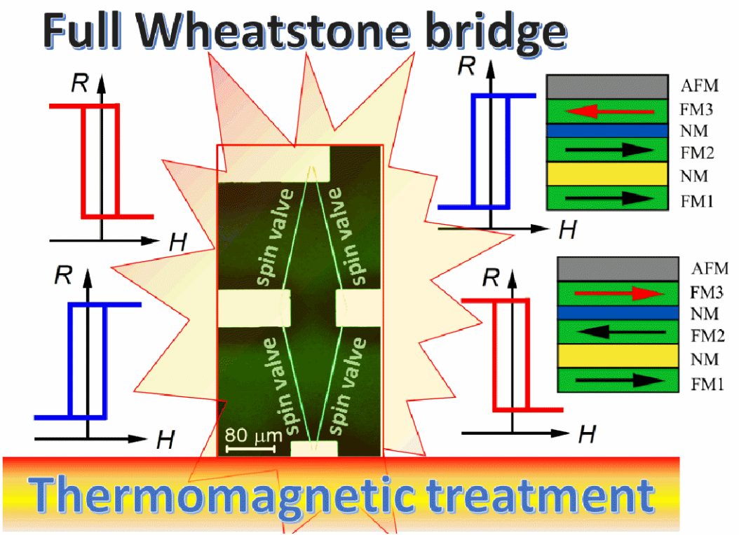
In this work the spin valves with a predominance of RKKY interaction between the free and reference layers are studying. The formation of an exchange shift in the pinned layer under combination of shape anisotropy and uniaxial anisotropy is investigated. A thermomagnetic treatment mode to form an opposite exchange shift in the non-parallel sides of a rhombus-shaped microobject was found and full Wheatstone bridge circuit was realized.
2. Materials and Methods
SVs with the composition Ta(5)/[Ni
80Fe
20]
60Cr
40(5)/Co
70Fe
20Ni
10(
tFL)/Cu(
tCu)/ Co
70Fe
20Ni
10(
tRL)/Ru(0.8)/Co
70Fe
20Ni
10(
tPL)/Fe
50Mn
50(18)/Ta(6) were deposited on glass substrates by dc magnetron sputtering in the magnetic field of 80 Oe applied in a film plane. Layer thicknesses are given in nm. The thicknesses of Cu and FM layers were varied. Co
70Fe
20Ni
10 was used as FM layer. For this alloy the saturation magnetization is 13% higher and the coercivity is 4.5 times lower than for Co
90Fe
10 commonly used in SVs [
16]. The buffer layer Ta/[Ni
80Fe
20]
60Cr
40 promotes the formation of <111> texture [
17,
18] and the decrease of crystallites size and interlayer roughness of nanostructured film [
19].
Studies of materials microstructure were carried out by X-ray diffractometry on a DRON-3M difactometer in CoKα1 radiation and by transmission electron microscopy on a Tecnai G-30.
Magnetic microstructure of microobjects was investigated by scanning probe microscope Solver Next (NT-MDT) in the magnetic force microscopy (MFM) mode.
Magnetoresistive measurements and TMT were carried out in a setup based on a Bruker electromagnet and a LakeShore 336 temperature controller. TMT involved heating in a helium atmosphere to a temperature
TTMT = 448 K, which exceeds the blocking temperature
Tb = 433 K for SVs based on an antiferromagnetic FeMn alloy [
20]. The magnetoresistance was determined as
MR = (
R(
H)
- Rs)/
Rs, where
R(
H) – resistance of the sample in a magnetic field,
Rs – resistance of the sample in the saturation field.
Microobjects were fabricated by laser lithography on DWL 66+ (Heidelberg Instruments Mikrotechnik GmbH) and reactive ion etching on PlasmaPro 80 RIE (Oxford Instruments)
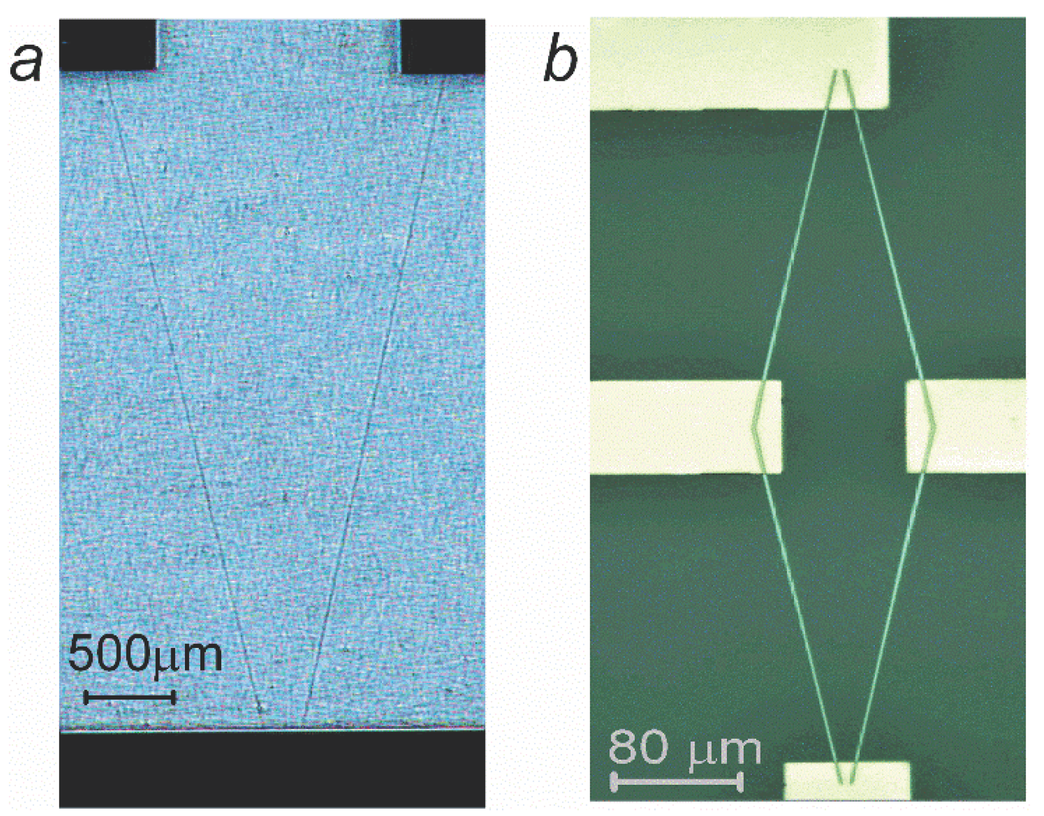
. The contact pads were fabricated using the lift-off procedure. There were prepared 2 types of microobjects (
Figure 1). (1) V-shaped microobjects were made of two microstripes forming a corner with Cu contact pads at the apex of the corner and at the ends of the microstripes. The corner angle (α ) was 20 or 40º, and its bisector was coincided with the EA. (2) Rhombus-shaped microobjects were made of 315 μm long and 2 μm wide microstripes and Cu pads at the rhombus vertices. The acute angles were α = 20 or 40º, and the long rhombus diagonal was coincided with the EA.
3. Results
3.1. Microstructural studies
The Co
70Fe
20Ni
10, [Ni
80Fe
20]
60Cr
40 ternary FM alloys, Cu and Fe
50Mn
50 antiferromagnetic alloy have the same cubic face-centered (fcc) crystal structure and similar lattice parameter values.
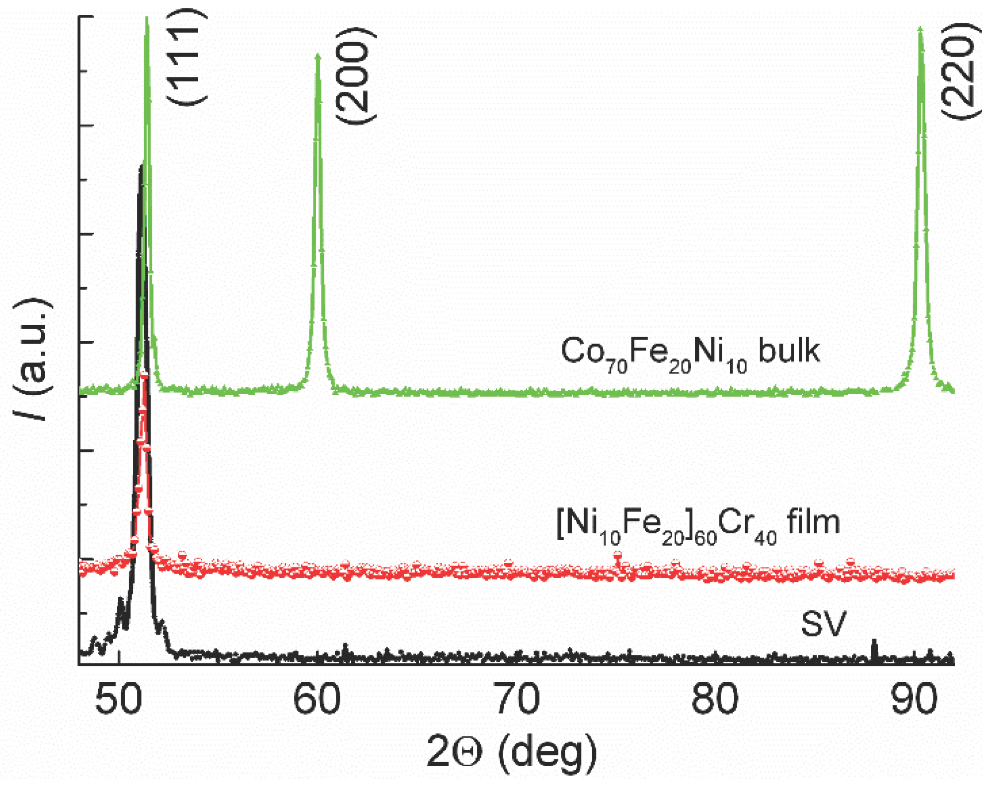
Figure 2 shows coincidence of the angular position of (111) peak for bulk Co
70Fe
20Ni
10 alloy, thin film of Co
70Fe
20Ni
10 alloy and for the SV containing the layers of these alloys. It is seen that there is <111> texture in the film and in the SV, since there are no other peaks of the fcc structure. The full width at half-maximum of the rocking curve (ω-scan) for (111) peak of SV is 4.4 degrees.
Thickness oscillations (satellites) are clearly seen around (111) peak in SV X-ray diffraction pattern. The thickness estimated by the period of these oscillations coincides with the total thickness of the NiFeCr/CoFeNi/Cu/CoFeNi layers of the SV. Thus in that part of nanostructure alignment of the microstructure of the layers takes place.
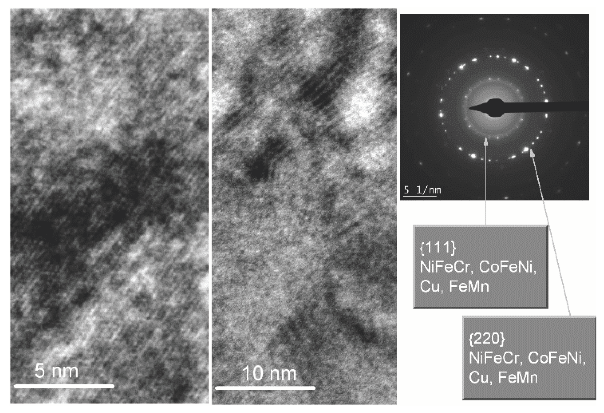
Figure 3 shows the results of TEM investigation. In electron diffraction pattern Debye rings for NiFeCr, CoFeNi, Cu and FeMn are common because of the same fcc structure and similar lattice parameter. Note that {220} ring is the brightest, and {111} ring is weak. This is characteristic for <111> texture and consistent with the results of the X-ray diffraction study. High-resolution images show thin parallel bands (
Figure 3a). It is direct resolution of atomic plane projections on the image plane.
Figure 3 b shows moire lines. This is the result of the interference of diffracted by the crystal lattices of adjacent layers electron beams. In multilayer structures such parallel to each other moire lines appear if the lattice mismatch of layers is low and the number of dislocations and packaging defects is small.
So, studied SVs have perfect microstructure of layers, low lattice mismatch of layers and high perfection of <111> texture. Such properties of microstructure were obtained by using layer materials with similar crystal structure and the buffer layer of the Ta(5)/NiFeCr(5) composition. In [
9,
19] the similar high-quality microstructure was achieved in superlattices and spin valves sputtered onto Ta/NiFeCr buffer layer. In present investigation, we need such microstructural properties to obtain smooth interfaces and RKKY interlayer coupling prevalence.
3.2. Exchange coupling of free and reference layers
Magnetoresistive curves were measured for SVs with various
tCu = 1.8 – 2.4 nm in a field applied parallel to PD || EA.
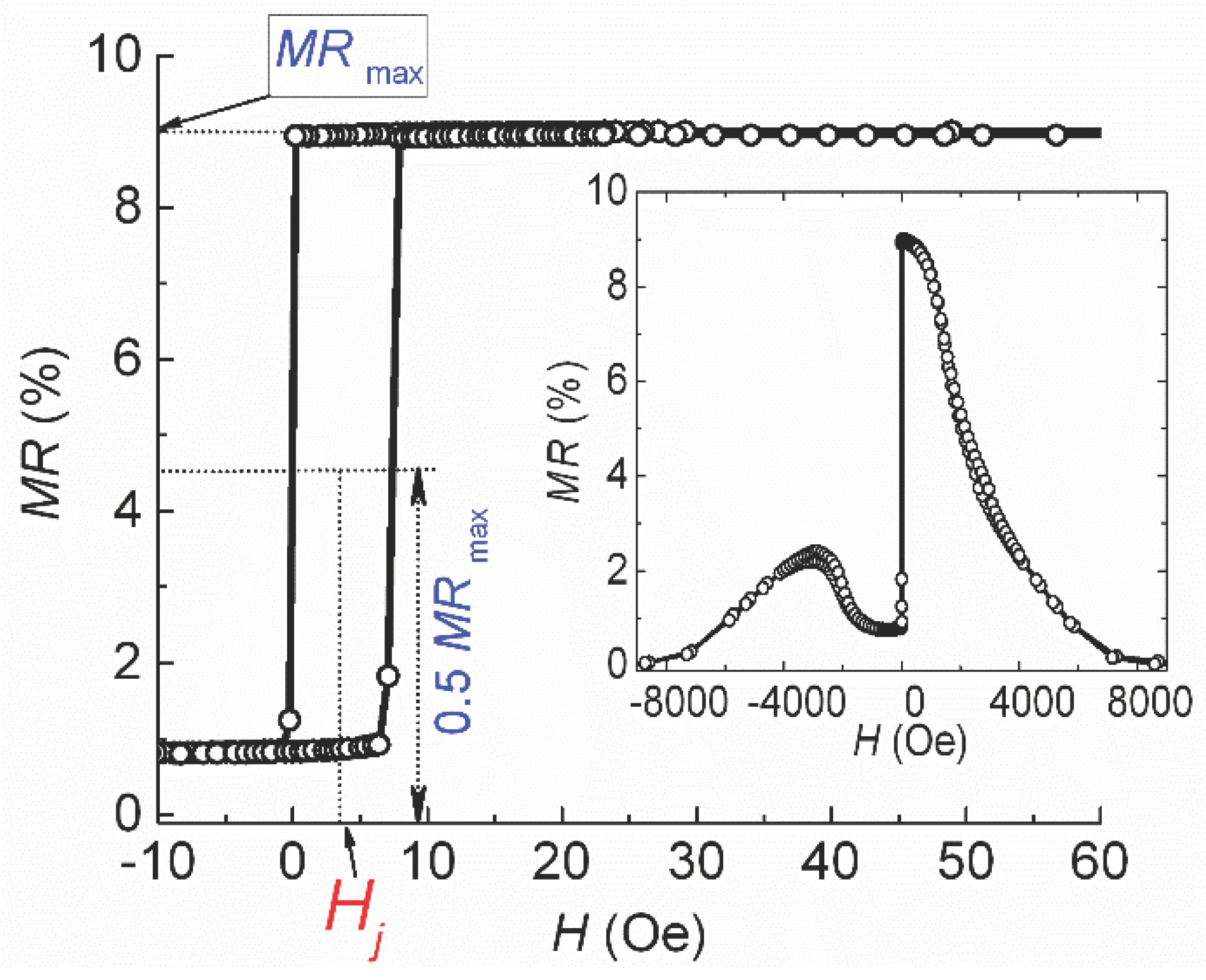
Figure 4 shows
MR(
H) curve for SV with
tCu = 2.2 nm. It is seen from the figure how the values of
MRmax and the shift of low field hysteresis loop (
Hj) were estimated.
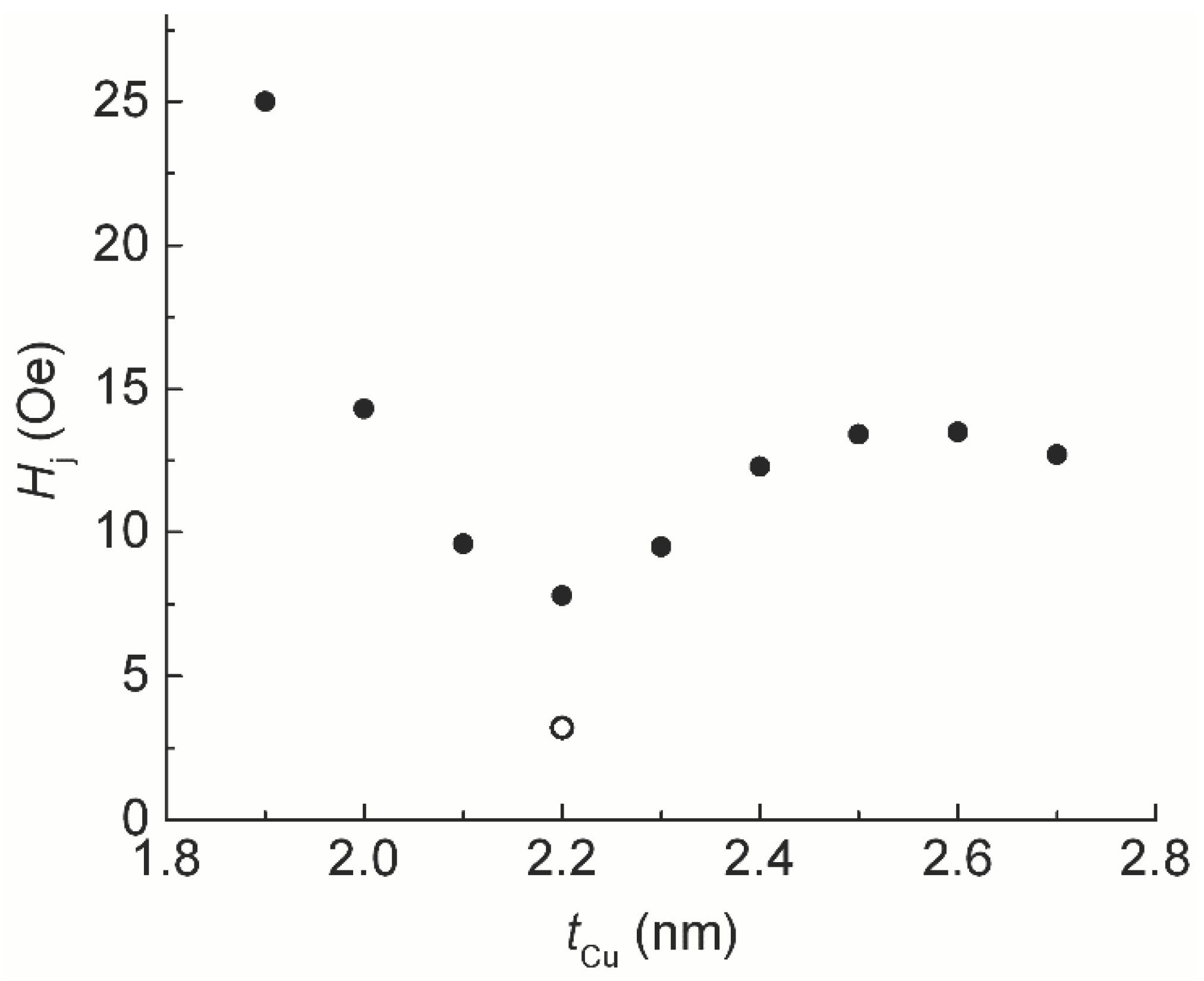
The
Hj value depends on the interaction between free and reference FM layers. Ordinarily, if the ferromagnetic dipolar coupling dominates, then
Hj(
tCu) dependence decreases monotonously. In our case
Hj(
tCu) dependence has an oscillating character, and we may conclude that RKKY interlayer coupling dominates (
Figure 5).
Minimum value of
Hj was obtained at
tCu = 2.2 nm. Then we changed the thickness of FM layers in order to increase
MRmax and further reduce the
Hj. We achieved the
Hj value close to
H = 0 (open symbol in the
Figure 5) and
MRmax = 9 % . In the SV of obtained composition, we changed the reference layer thickness (
tRL). Thus, the difference (
tRL –
tPL) between FM layers in SAF and the total magnetic moment of SAF changed, respectively.
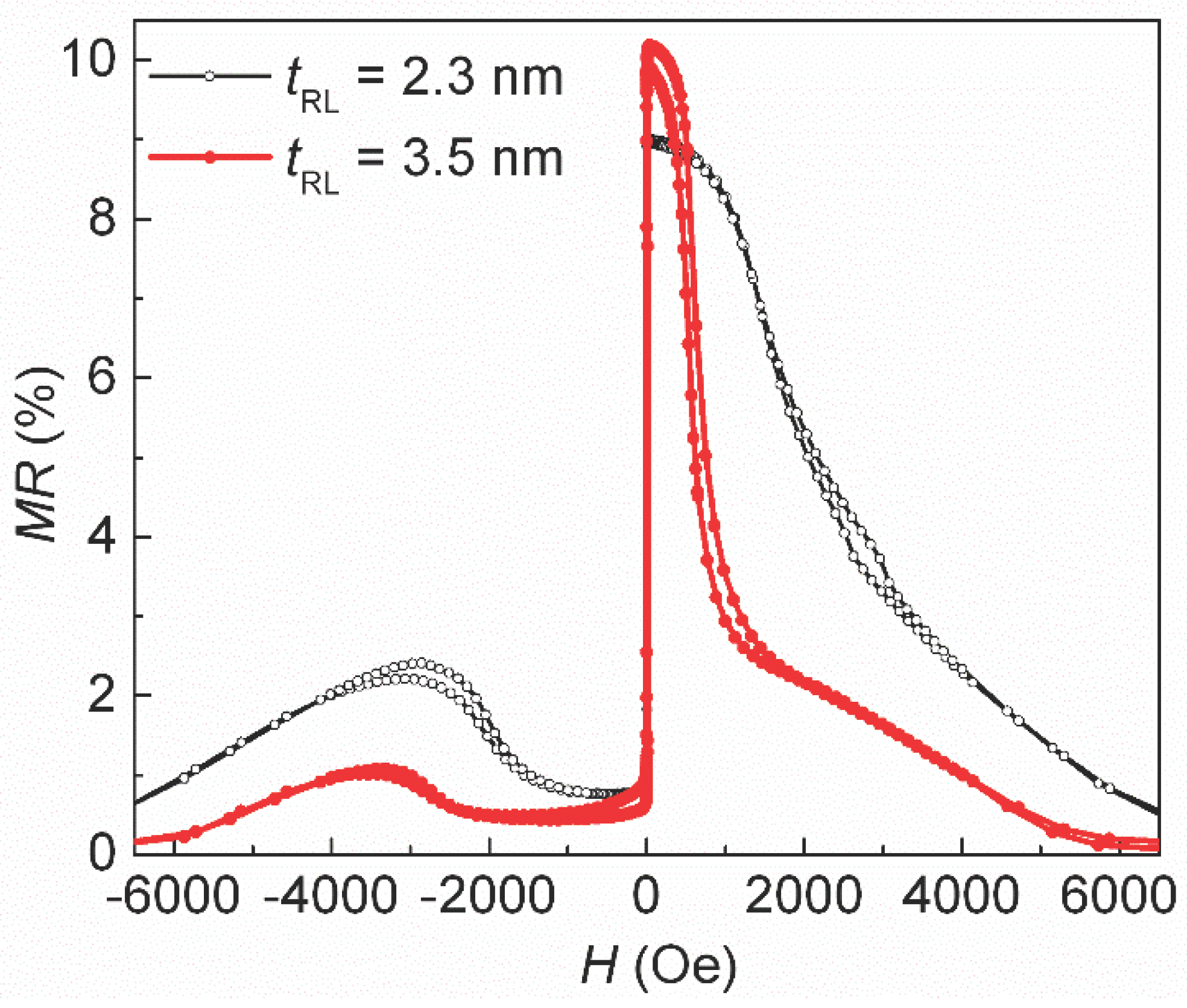
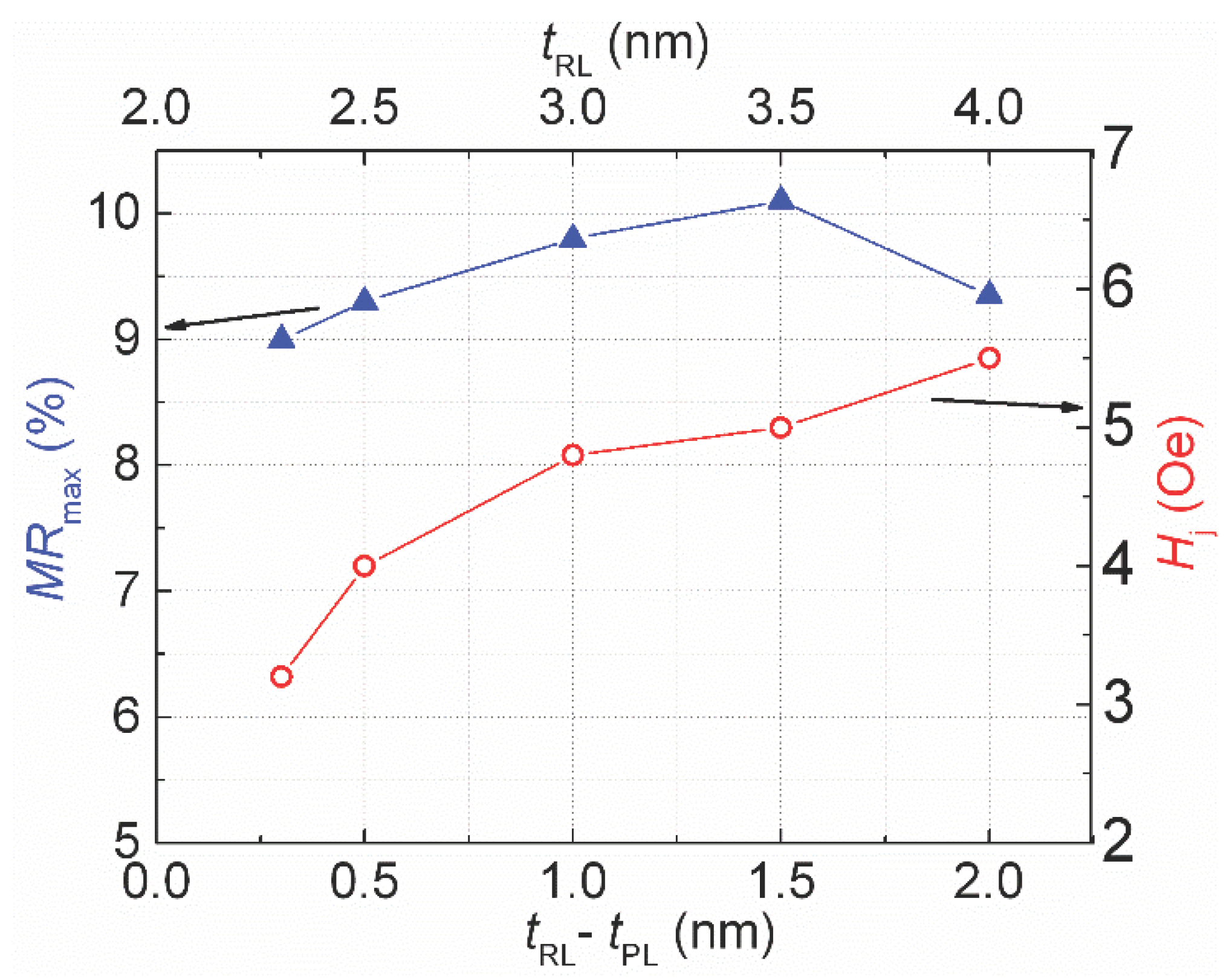
Figure 6 and
Figure 7 show change of magnetoresistive curves and the values of
Hj and
MRmax that occur due to increasing value of
tRL.
It can be seen that when the thickness and, accordingly, the magnetic moment of the reference layer increases, the interlayer coupling and the Hj value naturally increase. Note that the value of MRmax varies slightly.
Further studies will be carried out on this series of SVs with a small shift of the low-field hysteresis loop and different values of the reference layer magnetic moment.
3.3. Change of pinning direction in spin valve films and microobjects during thermomagnetic treatment
Thermomagnetic treatment procedure includes annealing at
TTMT and subsequent cooling in the applied magnetic field
HTMT. If
TTMT >
Tb, the exchange interaction at the boundary CoFeNi/FeMn is destroyed, then the initial unidirectional anisotropy and the initial PD in the SV disappear. Cooling in the applied magnetic field forms new unidirectional anisotropy and new PD1. The direction of PD1 coincides with direction of magnetic moment of adjacent FM layer [
21,
22]. We performed two consecutive TMT procedures for the following objects: V-shaped SV microobject and SV film. We performed the first TMT(1) in
HTMT = 9 kOe exceeding the magnetic saturation field and the second TMT(2) in
HTMT ≈ 0.
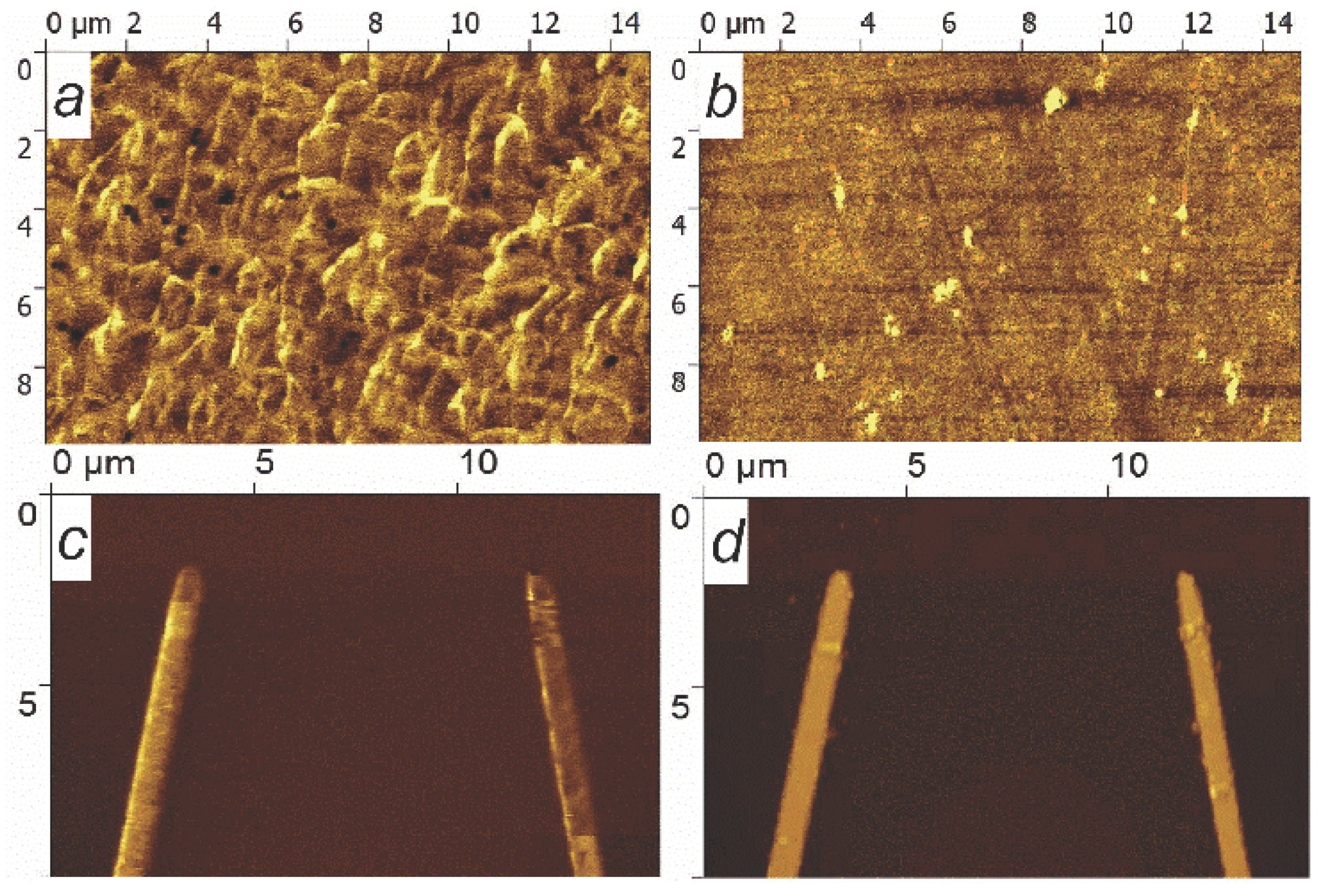
HTMT was always directed perpendicular to EA. After TMT(2) we investigated the magnetic structure of V-shaped microobject and SV film using magnetic force microscopy.
Figure 8 shows topography and corresponding MFM images obtained for the film and for V-shaped microobject.
The MFM image of the film shows an irregular magnetic structure. Each of the two stripes of the V-shaped microobject is in an almost single-domain state. Magnetic contrast shows that the magnetic ordering in these stripes is different. In MFM image (
Figure 8c) left stripe is lighter than right stripe while there is no such difference in the topography image. Thus, after the same TMT, different magnetic structures are formed in the film and in V-shaped microobject. Presumably, the reason of the observed differences is as follows.
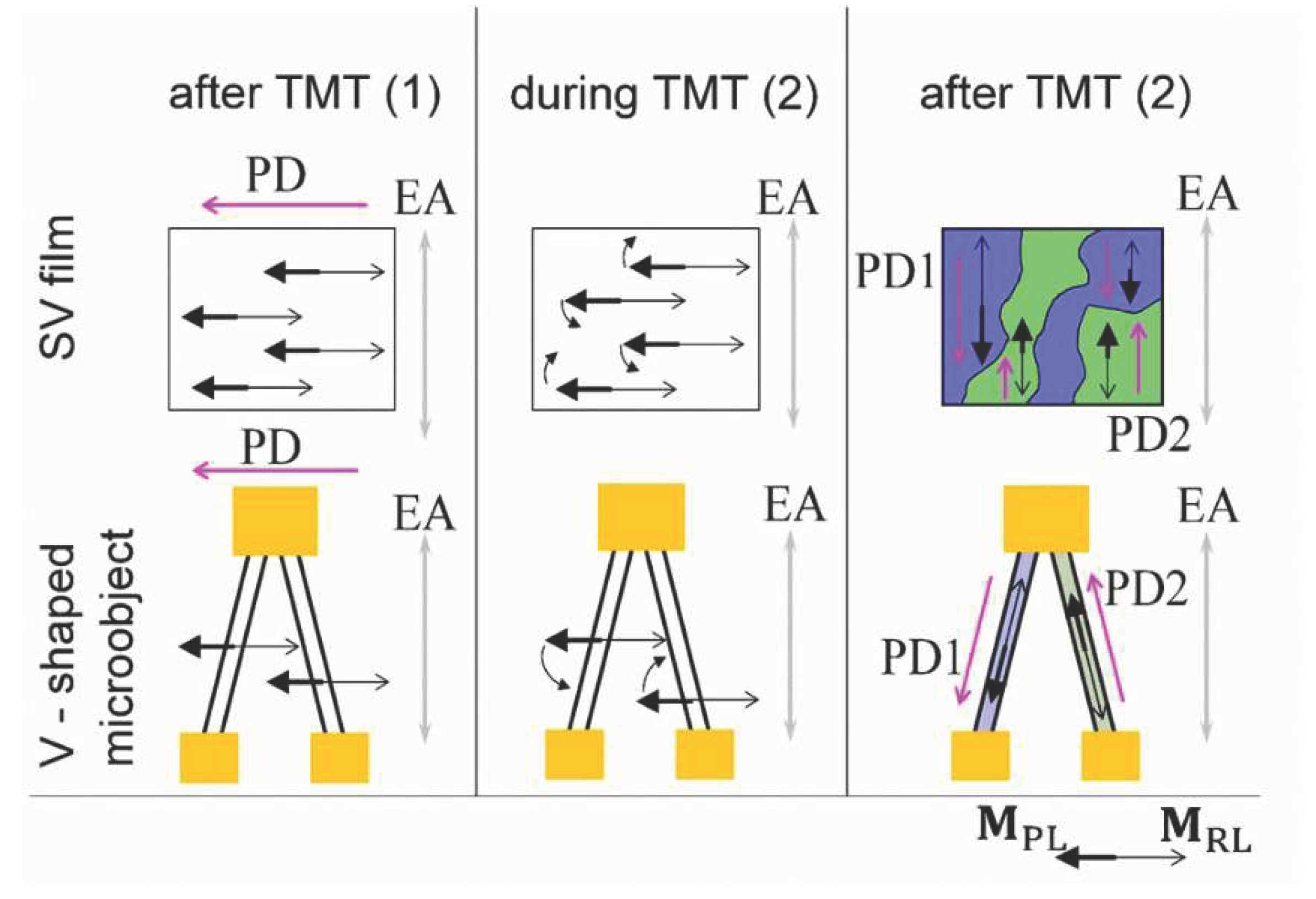
Magnetic moments of pinned and reference layer (
MPL and
MRL) are antiferromagnetically coupled and opposite to each other in
HTMT ≈ 0. In the SV film during TMT(2) at
T =
TTMT uniaxial anisotropy controls the turn of
MPL and
MRL, thus the clockwise and counterclockwise turns are equally probable (
Figure 9). During subsequent cooling, the exchange interaction in CoFeNi/FeMn boundary fixes this different magnetic ordering and forms new pinning directions PD1 and PD2 in different regions of the film. PD1 and PD2 are antiparallel and collinear with EA. In microobjects, shape anisotropy competes with uniaxial anisotropy. If shape anisotropy dominates, then it controls the turn of
MPL and
MRL during TMT(2) at
T =
TTMT. With our experiment geometry (
Figure 9) in one stripe of V-shaped microobject
MPL and
MRL will turn clockwise, and in the other – counterclockwise. Thus after the cooling new pinning directions PD1and PD2 are collinear with stripes. If the angle between the stripes is 20 or 40
o, the angle between PD1 and PD2 will be 160 or 140
o, respectively.
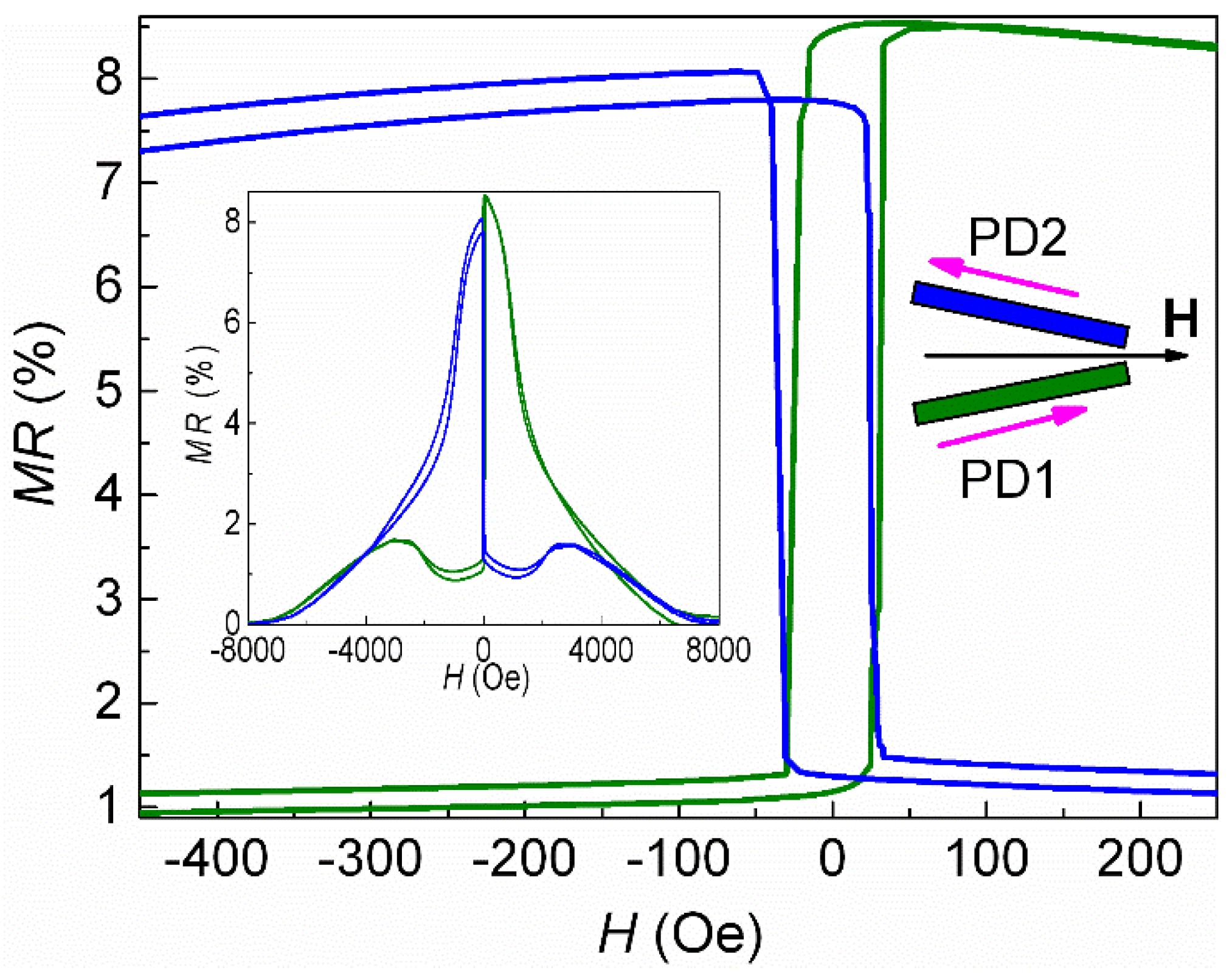
Magnetoresistive curves measured for each stripe of V-shaped microobject in the magnetic field applied parallel to EA are shown in
Figure 10. The values of
Hex for two different stripes are opposite in sign. This is in a good agreement with the fact that in one stripe the projection of PD onto the applied field is positive, and in the other - negative.
In the low fields dMR/dH > 0 for the green magnetoresistive curve and dMR/dH < 0 for the blue magnetoresistive curve. Note that this PD arrangement was obtained in different stripes of a single microobject by two TMT in a direction-fixed magnetic field.
3.4. Full Wheatstone Bridge based on rhombus-shaped spin valve microobject
TMT(1) and TMT(2) procedures were performed for rhombus-shaped spin valve microobject.
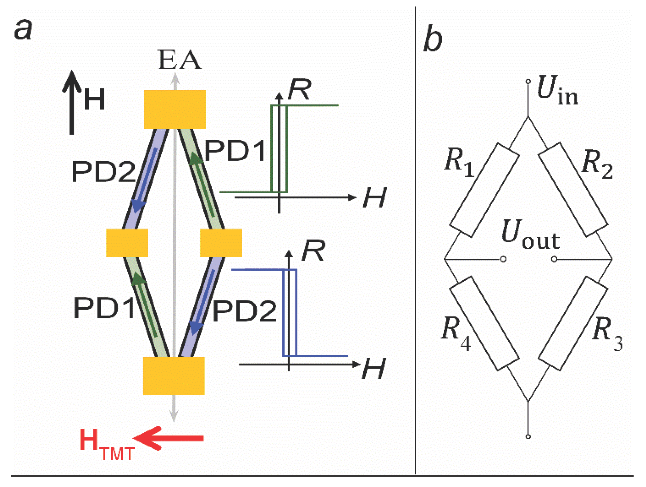
Figure 11 shows the PD arrangement in rhombus sides which can be expected if you consider a rhombus as two V-shaped microobjects. It is this mutual PD arrangement that is required to implement the Wheatstone bridge, in which d
R1,3/d
H and d
R2,4/d
H are opposite in sign, thus each SV-element makes an active contribution to the output signal.
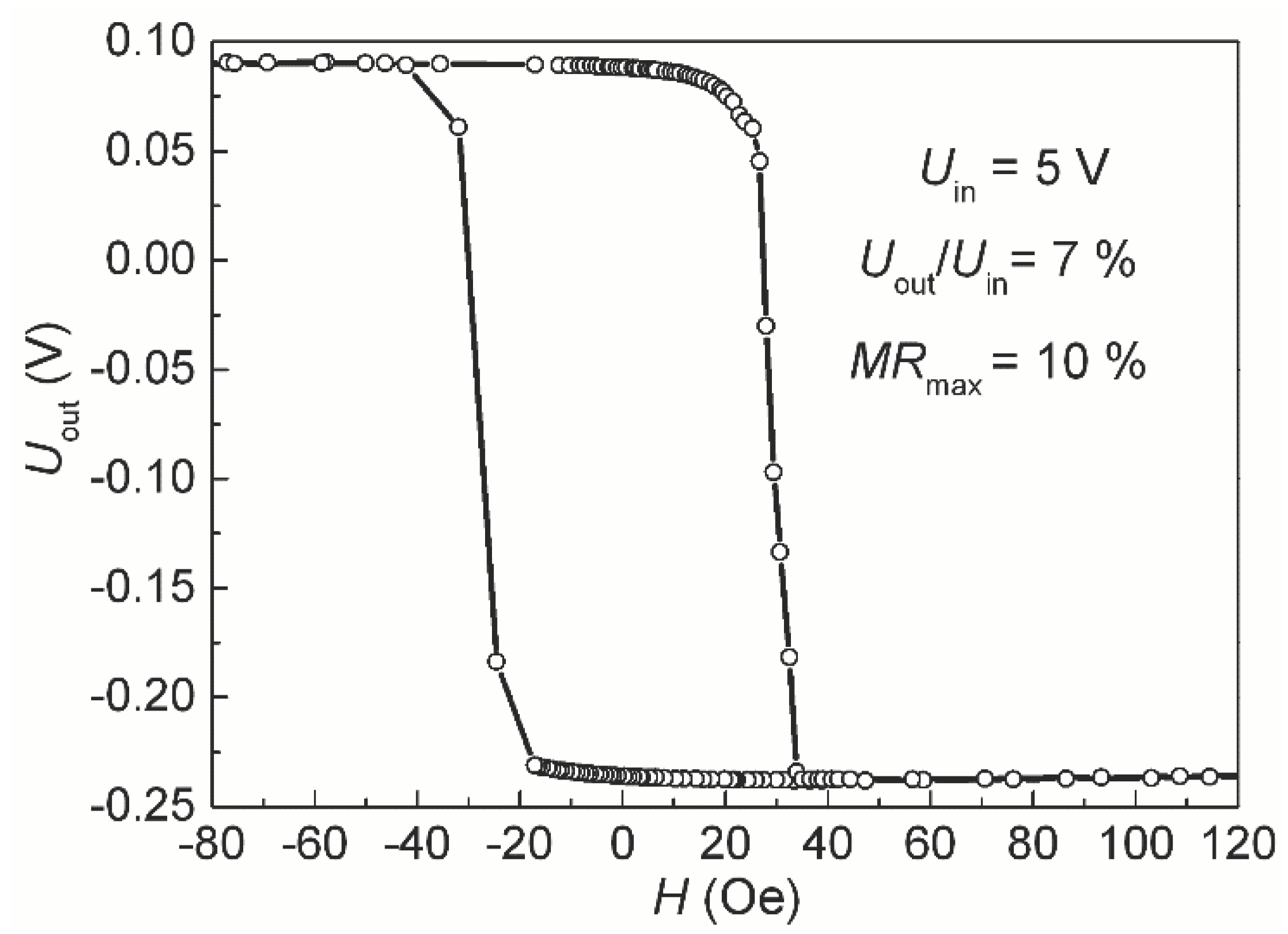
We applied supply voltage (
Uin) to the long diagonal and measured output voltage (
Uout) in the short diagonal of the rhombus under a magnetic field swept along EA (
Figure 12).
Maximal output of full Wheatstone bridge is estimated from
Uout/
Uin = Δ
R/
R, where
R is the resistance of each of the four elements and Δ
R is a resistance change in the applied magnetic field. For half Wheatstone bridge with two active sensing elements, maximal output is
Uout/
Uin = 0.5Δ
R/
R, accordingly [
23]. Thus, for full Wheatstone bridge with for active SV-elements we obtain
Uout/
Uin =
MRmax, where
MRmax is maximal magnetoresistance of each SV-element. In our case
Uout/
Uin = 7 % while
MRmax = 10 % (
Figure 6 and
Figure 12), thus 0.5
MRmax <
Uout/
Uin <
MRmax. A possible reason is that there are small areas of undesirable PD orientation in the rhombus -forming stripes. These areas are visible in the image of the magnetic structure (
Figure 8c) in the upper part of the left stripe and in the lower part of the right stripe.
3.5. Formation of opposite pinning directions in rhombus-shaped microobjects based on spin valves with different thickness of the reference layer
An increase in the thickness
tRL leads to an increase of the total effective magnetic moment (
Meff) of antiferromagnetically coupled
MPL and
MRL,
Meff =
MRL -
MPL. During TMT(2) at
T >
Tb the magnetic moments arrange in accordance to minimize the anisotropy energy. We estimate the shape anisotropy field, using [
24] where the demagnetizing factors of the general ellipsoid were reported. For the long stripe, the demagnetizing factor is approximately
t/
w, where
t is the thickness of the FM layer and
w is the width of the stripe. Hence, the anisotropy field is the sum of two terms:
Ha = 2
Ku/
Meff + 4
Meff t/
w, where
Ku is uniaxial anisotropy constant and
t =
tRL +
tPL. We change the relationship between the two terms of the anisotropy field by changing
tRL. Thus, we can change the magnetic moments arrange after TMT(2).
Rhombus-shaped microobjects with the angle α = 20 and 40
o were fabricated from the films of SVs with
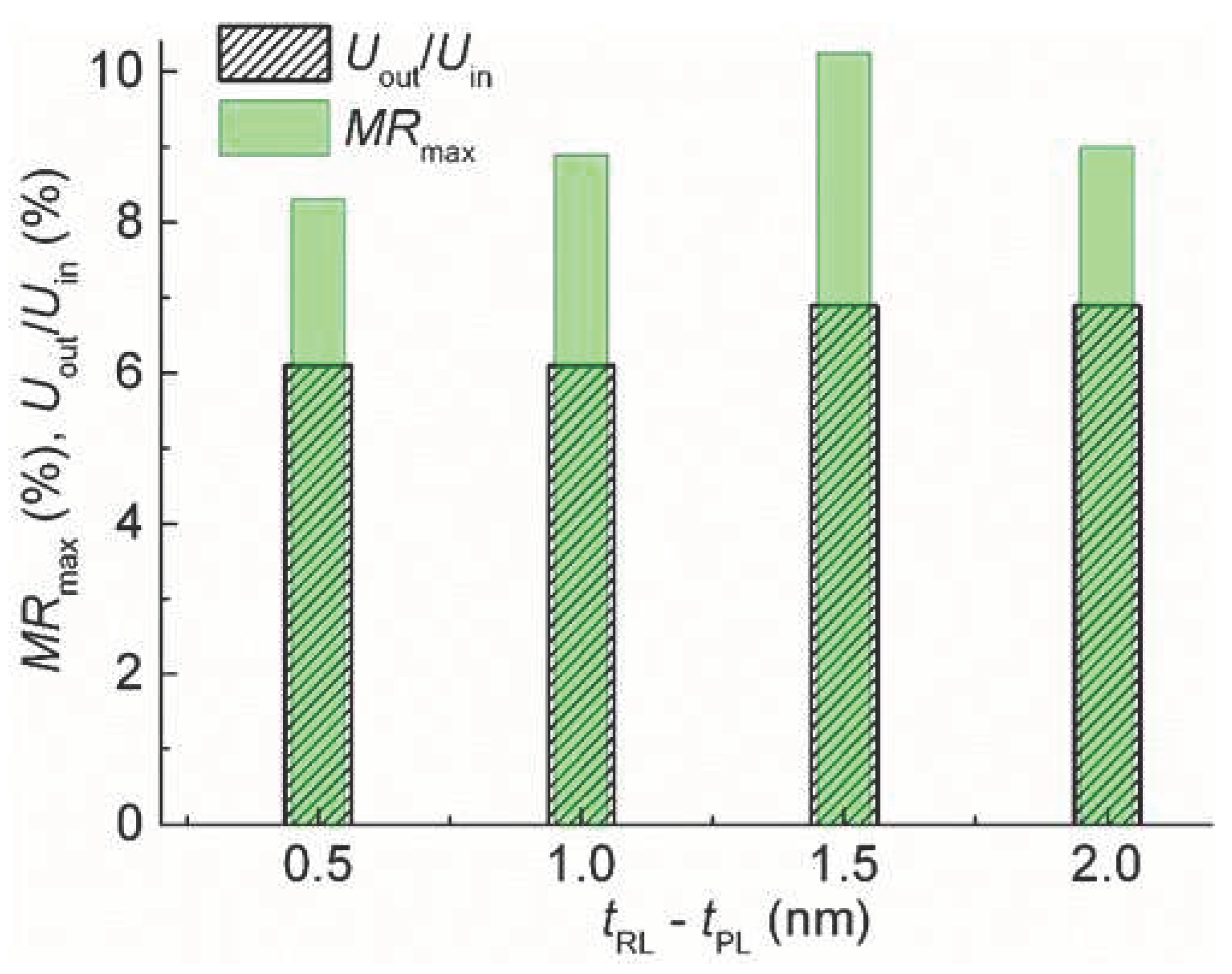
tRL = 2.3, 2.5, 3.0, 3.5 and 4 nm. TMT(1) and TMT(2) were performed consistently and then the Wheatstone bridge output voltage was measured in the short diagonal of the rhombus under a magnetic field swept along EA.
Figure 13 shows the bar charts for comparison of the Wheatstone bridge
Uout/
Uin ratio with the
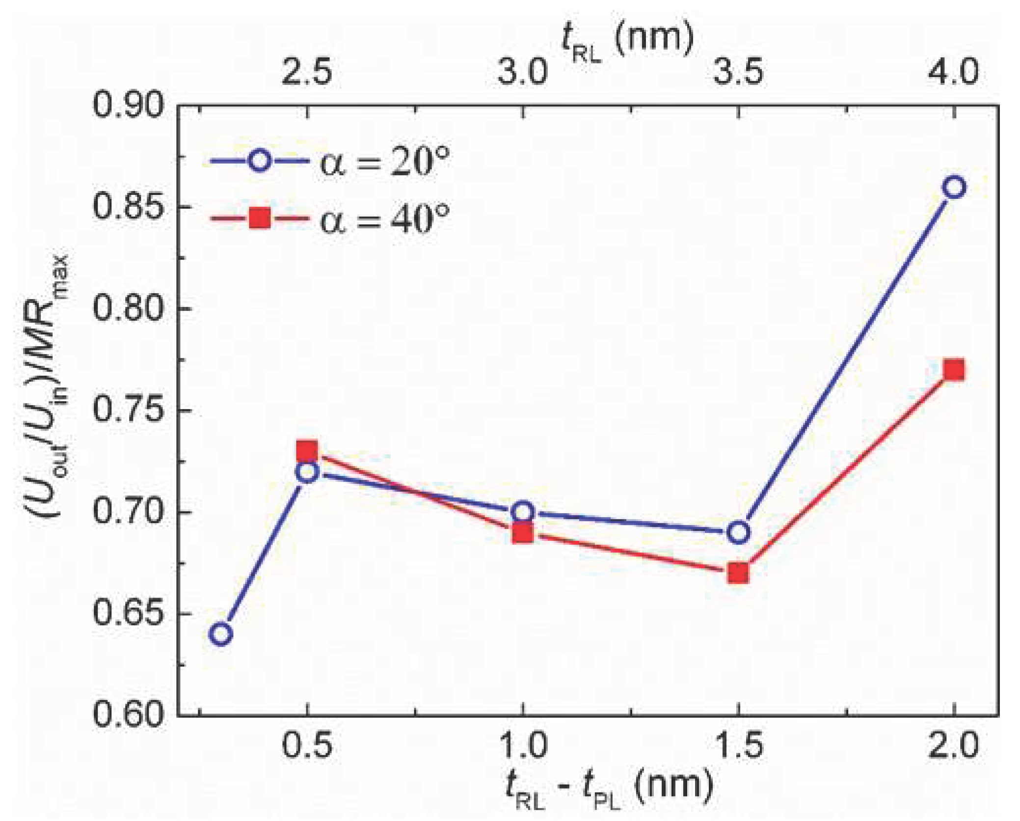
MRmax value of SV stripes. For the convenience of the comparison we also plotted the relation between
Uout/
Uin and
MRmax as a function of the reference layer thickness (
Figure 14).
For two sets of the rhombus-shaped microobjects (α = 20 and 40o) the minimal difference between Uout/Uin and MRmax was found for samples with maximum tRL and maximum difference in FM layers thicknesses in SAF. Probably, the effect of shape anisotropy on the alignment of magnetic moments at TMT increases with an increase in the total magnetic moment of antiferromagnetically coupled MPL and MRL.
4. Discussion
The proposed method of implementing the full Wheatstone bridge scheme with SVs as a magnetically sensitive material is quite simple. It does not require separate sputtering of SV elements with an exchange bias opposite in sign and separate TMT of each SV element. Nevertheless, there are a number of requirements for the successful application of this method. To prevent accidental splitting into magnetic domains, the microstructure of the layers should contain a minimum of defects and the interlayer boundaries should be smooth. Opposite in exchange bias SV elements should change magnetoresistance in the same low fields. Therefore, the shift of the low-field hysteresis loop should be close to H = 0. To increase the ratio between Uout/Uin and MRmax of each SV element, it is necessary to increase the difference in the thicknesses of the reference and pinned layer and, accordingly, the total magnetic moment of SAF
5. Conclusions
It is shown that shape anisotropy controls turn of magnetic moments in spin valve microobjects in low magnetic fields.
We found the TMT procedure, which makes it possible to obtain opposite in sign exchange bias fields and a close to collinear arrangement of axes of uniaxial and unidirectional anisotropy in separate elements of Wheatstone bridge circuit. The procedure includes two subsequent TMT in the applied perpendicular to easy axis magnetic field. At the first TMT the field exceed the saturation field and at the second TMT the field is close to H = 0. Formation of the opposite exchange bias in non-parallel sides of the rhombus-shaped microobject is caused by the predominance of shape anisotropy in magnetic reversal and during TMT. Output signal of the based on the complete Wheatstone Bridge sensor have the shape of a step. Such characteristic are in demand in switching devices.
Author Contributions
V.U. supervision and project administration , V.P. magnetron sputtering SV films, L.N. design of experiments and analysis of the data, writing of manuscript, X-ray diffractometry, A.G. mi-croobjects fabrication, magnetoresistance measurements, T.C. investigation, thermomagnetic threatment, figure representations and analysis of the data, A.P. magnetic microscopic investiga-tion by atomic force microscopy , T.K. microstructure studies by transmission electron micros-copy, M.M. supervision, review and editing. All authors have read and agreed to the published version of the manuscript.
Funding
This study was performed in terms of state assignment for the Ministry of Science and Higher Education of the Russian Federation (theme Spin, no. 122021000036-3).
Institutional Review Board Statement
Not applicable.
Informed Consent Statement
Not applicable
Conflicts of Interest
The authors declare no conflict of interest.
References
- Freitas, P.P.; Ferreira, R.; Cardoso, S. Spintronic sensors. Proceeding of the IEEE 2016, 104, 1894–1918. [Google Scholar] [CrossRef]
- Carvalho, M.; Ribeiro, P.; Romão, V.; S. Cardoso, S. Smart fingertip sensor for food quality control: Fruit maturity assessment with a magnetic device. Journal of Magnetism and Magnetic Materials 2021, 536, 168116. [CrossRef]
- Yan, S.; Cao, Z.; Guo, Z.; Zheng, Z.; Cao, A.; Qi, Y.; Leng, Q.; Zhao, W. Design and Fabrication of Full Wheatstone-Bridge-Based Angular GMR Sensors. Sensors 2018, 18, 1832. [Google Scholar] [CrossRef] [PubMed]
- Suharyadi, E.; Alfansuri, T.; Handriani, L. S.; Wibowo, N. A.; Sabarman, H. Detection of Fe3O4/PEG nanoparticles using one and two spin-valve GMR sensing elements in Wheatstone bridge circuit. Journal of Materials Science: Materials in Electronics 2021, 32, 23958–23967. [Google Scholar] [CrossRef]
- Dieny, B.; Speriosu, V.S.; Parkin, S.S.P.; Gurney, B.A.; Wilhout, D.R.; Maui, D. Giant magnetoresistance in soft ferromagnetic multilayers. Phys. Rev. B. 1991, 43, 1297–1300. [Google Scholar] [CrossRef] [PubMed]
- Kools, J.C.S. Exchange-Biased Spin-Valves for Magnetic Storage. IEEE Trans. on Magn. 1996, 32, 3165–3184. [Google Scholar] [CrossRef]
- Svalov, A.V.; Sorokin, A.N.; Savin, P.A.; García-Arribas, A.; Fernández, A.; Vas’kovskiy, V.O.; Kurlyandskaya, G.V. Co/Cu/Co Pseudo Spin-Valve System Prepared by Magnetron Sputtering with Different Argon Pressure. Key Engineering Materials 2015, 644, 211–214. [Google Scholar] [CrossRef]
- Öksüzoglu, R.M.; Sarac, U. , Yıldırım M., Çınar H. Characterization of Microstructural and Morphological Properties in As-deposited Ta/NiFe/IrMn/CoFe/Ta Multilayer. System. J. Mater. Sci. Technol. 2014, 30, 359–364. [Google Scholar] [CrossRef]
- Naumova, L.I.; Milyaev, M. A.; Zavornitsin, R. S.; Pavlova, A. Yu.; Maksimova, I. K.; Krinitsina, T. P.; Chernyshova, T. A.; Proglyado, V. V.; Ustinov, V. V. High-Sensitive Sensing Elements Based on Spin Valves with Antiferromagnetic Interlayer. Coupling. Physics of Metals and Metallography 2019, 120, 653–659. [Google Scholar] [CrossRef]
- Meguro, K.; Hoshiya, H.; Watanabe, K.; Hamakawa, Y.; Fuyama, M. Spin-Valve Films Using Synthetic Ferrimagnets for Pinned Layer. IEEE Trans. on Magn. 1999, 35, 2925–2927. [Google Scholar] [CrossRef]
- Huai, Y.; Zhang, J.; Anderson, G.W.; Rana, P.; Funada, S.; Hung, C.Y.; Zhao, M.; Tran, S. Spin-valve heads with synthetic antiferromagnet CoFe/Ru/CoFe/IrMn. Journal of Applied Physics 1999, 85, 5528–5530. [Google Scholar] [CrossRef]
- Milyaev, M.; Naumova, L.; Chernyshova, T.; Proglyado, V.; Kamensky, I.; Ustinov, V. Spin-flop in Synthetic Antiferromagnet and Anhysteretic Magnetic Reversal in FeMn-Based Spin Valves. IEEE Trans. on Magn. 2016, 52, 2301104. [Google Scholar] [CrossRef]
- Milyaev, M.A.; L. I. Naumova, L.I.; Zavornitsyn, R.S.; Maksimova, I.K.; A.Yu. Pavlova, A.Yu.; Proglyado, V.V.; Ustinov, V.V. Use of a Spin-Flop State for the Creation of Spin-Valve Elements for a Full Wheatstone Bridge. Physics of Metals and Metallography 2020, 121, 721–728. [Google Scholar] [CrossRef]
- Ferreira, R.; Paz, E.; Freitas, P.; Ribeiro, J.; Germano, J.; Sousa, L. 2-Axis Magnetometers Based on Full Wheatstone Bridges Incorporating. Magnetic Tunnel Junctions Connected in Series. IEEE Trans. on Magn. 2012, 48, 4107. [Google Scholar] [CrossRef]
- Borole, U.P.; Khan, J.; Barshilia, H.C.; Chowdhury, P. Design, fabrication, and characterization of giant magnetoresistance (GMR) based open-loop current sensor with U-shaped current carrying conductor. Sensors Actuators A 2021, 332, 112103. [Google Scholar] [CrossRef]
-
Fukuzawa H., Iwasaki H., Koi K., Sahashi M. Soft magnetic characteristics of an ultrathin CoFeNi free layer in spin-valve films J. Magnetism and Magnetic Mater 2006, 298, 65–71. [CrossRef]
- Sugita, Y.; Kawawake, Y.; Satomi, M.; Sakakima, H. Thermal stability of PtMn based synthetic spin valves using thin oxide layer. J. Appl,. Phys. 2001, 89, 6919–6921. [Google Scholar] [CrossRef]
- Bannikova, N. S.; Milyaev, M. A.; Naumova, L. I.; Patrakov, E. I.; Proglyado, V. V.; Kamenskii, I. Yu.; Ryabukhina, M. V.; Ustinov, V. V. Giant Magnetoresistance and Hysteresis Phenomena in CoFe/Cu Superlattices with Highly Perfect Crystallographic Texture. Physics of Metals and Metallography 2018, 119, 1073–1078. [Google Scholar] [CrossRef]
- Bannikova, N. S.; Milyaev, M. A.; Naumova, L. I.; Krinitsina, T. P.; Patrakov, E. I.; Proglyado, V. V.; Chernyshova, T. A.; Ustinov, V. V. NiFeCo/Cu superlattices with high magnetoresistive sensitivity and weak hysteresis. Physics of the Solid State 2016, 58, 2011–2017. [Google Scholar] [CrossRef]
- Berkowitz, A.E.; Takano, K. Exchange anisotropy - a review. J. Magn. Magn. Mat. 1999, 200, 552–570. [Google Scholar] [CrossRef]
- Tong, H.C.; Qian, C.; Miloslavsky, L.; Funada, S.; Shi, X.; Liu, F.; Dey, S. The spin flop of synthetic antiferromagnetic films J. Appl. Phys. 2000, 87, 5055–5067. [Google Scholar] [CrossRef]
- Beach, R.S.; McCord, J.; Webb, P.; Mauri, D. Orthogonal pinning of two ferromagnetic layers in a synthetic spin valve Appl. Phys. Lett. 2002, 80, 4576–4578. [Google Scholar] [CrossRef]
- Reig, C.; Cubells-Beltran, M.-D.; Munoz, D.R. ; Magnetic Field Sensors Based on Giant Magnetoresistance (GMR) Technology: Applications in Electrical Current Sensing. Sensors 2009, 9, 7919–7942. [Google Scholar] [CrossRef] [PubMed]
- Osborn, J.A. Demagnetizing Factors of the General Ellipsoid. Phys. Rev. 1945, 67, 351–357. [Google Scholar] [CrossRef]
Figure 1.
Images of V-shaped (a) and rhombus-shaped (b) microobject with contact pads.
Figure 1.
Images of V-shaped (a) and rhombus-shaped (b) microobject with contact pads.
Figure 2.
X-ray diffraction patterns for SV of Ta(5)/NiFeCr(5)/CoFeNi(3.5)/Cu(3.3)/CoFeNi(3.5) /Ru(0.8)/CoFeNi(3)/FeMn(10)/Ta(5) composition, NiFeCr film with thickness of 60 nm and bulk sample of CoFeNi alloy.
Figure 2.
X-ray diffraction patterns for SV of Ta(5)/NiFeCr(5)/CoFeNi(3.5)/Cu(3.3)/CoFeNi(3.5) /Ru(0.8)/CoFeNi(3)/FeMn(10)/Ta(5) composition, NiFeCr film with thickness of 60 nm and bulk sample of CoFeNi alloy.
Figure 3.
TEM high-resolution images and electron diffraction pattern for SV of Ta(5)/NiFeCr(5)/CoFeNi(3.5)/Cu(3.3)/CoFeNi(3.5)/Ru(0.8)/CoFeNi(3)/FeMn(10)/Ta(5) composition.
Figure 3.
TEM high-resolution images and electron diffraction pattern for SV of Ta(5)/NiFeCr(5)/CoFeNi(3.5)/Cu(3.3)/CoFeNi(3.5)/Ru(0.8)/CoFeNi(3)/FeMn(10)/Ta(5) composition.
Figure 4.
Low field part of magnetoresistive curve for SV of Ta(5)/NiFeCr(5)/CoFeNi(5.5)/Cu(2.2)/ CoFeNi(2.3)/Ru(0.8)/CoFeNi(2)/ FeMn(10)/Ta(5) composition. The inset shows the MR(H) curve in a wide range of fields.
Figure 4.
Low field part of magnetoresistive curve for SV of Ta(5)/NiFeCr(5)/CoFeNi(5.5)/Cu(2.2)/ CoFeNi(2.3)/Ru(0.8)/CoFeNi(2)/ FeMn(10)/Ta(5) composition. The inset shows the MR(H) curve in a wide range of fields.
Figure 5.
The dependence of low field hysteresis loop shift on the thickness of Cu layer for SVs of Ta(5)/NiFeCr(5)/CoFeNi(4)/Cu(tCu)/CoFeNi(4)/Ru(0.8)/CoFeNi(3.5)/FeMn(10)/Ta(5) composition (solid symbols) and the shift of low field hysteresis loop for the SV of Ta(5)/NiFeCr(5)/CoFeNi(5.5)/Cu(2.2)/CoFeNi(2.3)/Ru(0.8)/CoFeNi(2)/ FeMn(10)/Ta(5) composition (open symbol).
Figure 6.
Magnetoresistive curves for SVs of Ta(5)/NiFeCr(5)/CoFeNi(5.5)/Cu(2.2)/ CoFeNi(tRL)/Ru(0.8)/CoFeNi(2)/ FeMn(10)/Ta(5) composition for tRL = 2.3 and 3.5 nm.
Figure 6.
Magnetoresistive curves for SVs of Ta(5)/NiFeCr(5)/CoFeNi(5.5)/Cu(2.2)/ CoFeNi(tRL)/Ru(0.8)/CoFeNi(2)/ FeMn(10)/Ta(5) composition for tRL = 2.3 and 3.5 nm.
Figure 7.
Dependencies of low field hysteresis loop shift and the maximal magnetoresistance on the reference layer thickness for the SVs of Ta(5)/NiFeCr(5)/CoFeNi(5.5)/Cu(2.2)/ CoFeNi(tRL)/Ru(0.8)/CoFeNi(2)/ FeMn(10)/Ta(5) composition.
Figure 7.
Dependencies of low field hysteresis loop shift and the maximal magnetoresistance on the reference layer thickness for the SVs of Ta(5)/NiFeCr(5)/CoFeNi(5.5)/Cu(2.2)/ CoFeNi(tRL)/Ru(0.8)/CoFeNi(2)/ FeMn(10)/Ta(5) composition.
Figure 8.
Topography (b,d) and MFM (a,c) images obtained for the film (a,b) and for V-shaped microobject (c,d).
Figure 8.
Topography (b,d) and MFM (a,c) images obtained for the film (a,b) and for V-shaped microobject (c,d).
Figure 9.
Schematic representation of turn of reference and pinned layer magnetic moments in SV film and SV microobject during TMT.
Figure 9.
Schematic representation of turn of reference and pinned layer magnetic moments in SV film and SV microobject during TMT.
Figure 10.
Low field parts of magnetoresistive curves measured for each stripe of V-shaped SV microobject. The applied magnetic field direction with respect to PD1 and PD2 is shown in the insert on the right. The inset on the left shows the MR(H) curves in a wide range of fields. .
Figure 10.
Low field parts of magnetoresistive curves measured for each stripe of V-shaped SV microobject. The applied magnetic field direction with respect to PD1 and PD2 is shown in the insert on the right. The inset on the left shows the MR(H) curves in a wide range of fields. .
Figure 11.
Scheme of PD arrangement in rhombus-shaped microobject sides after TMT(1) and TMT(2) (a) and electric circuit of the Wheatstone bridge (b). The inset in (a) shows R(H) dependences for R1, R3 (blue) and R2, R4 (green).
Figure 11.
Scheme of PD arrangement in rhombus-shaped microobject sides after TMT(1) and TMT(2) (a) and electric circuit of the Wheatstone bridge (b). The inset in (a) shows R(H) dependences for R1, R3 (blue) and R2, R4 (green).
Figure 12.
Wheatstone bridge output under a magnetic field sweep along EA for the rhombus-shaped microobject based on SV of Ta(5)/NiFeCr(5)/CoFeNi(5.5)/Cu(2.2)/CoFeNi(3.5)/ Ru(0.8)/CoFeNi(2)/ FeMn(10)/Ta(5) composition.
Figure 12.
Wheatstone bridge output under a magnetic field sweep along EA for the rhombus-shaped microobject based on SV of Ta(5)/NiFeCr(5)/CoFeNi(5.5)/Cu(2.2)/CoFeNi(3.5)/ Ru(0.8)/CoFeNi(2)/ FeMn(10)/Ta(5) composition.
Figure 13.
The dependencies of Wheatstone bridge Uout/Uin ratio and SV stripe MRmax value on the thickness of the reference layer for rhombus-shaped microobjects with α = 40o.
Figure 13.
The dependencies of Wheatstone bridge Uout/Uin ratio and SV stripe MRmax value on the thickness of the reference layer for rhombus-shaped microobjects with α = 40o.
Figure 14.
The dependencies of the relation between Uout/Uin and MRmax on the thickness of the reference layer for rhombus-shaped microobjects with α = 20 and 40o.
Figure 14.
The dependencies of the relation between Uout/Uin and MRmax on the thickness of the reference layer for rhombus-shaped microobjects with α = 20 and 40o.
|
Disclaimer/Publisher’s Note: The statements, opinions and data contained in all publications are solely those of the individual author(s) and contributor(s) and not of MDPI and/or the editor(s). MDPI and/or the editor(s) disclaim responsibility for any injury to people or property resulting from any ideas, methods, instructions or products referred to in the content. |
© 2023 by the authors. Licensee MDPI, Basel, Switzerland. This article is an open access article distributed under the terms and conditions of the Creative Commons Attribution (CC BY) license (http://creativecommons.org/licenses/by/4.0/).
