Submitted:
04 January 2024
Posted:
04 January 2024
You are already at the latest version
Abstract
Keywords:
1. Introduction
2. Materials and Methods
3. Results and Discussion
Conclusion
Financial Support
References
- Whiteside, Mark, and J. Marvin Herndon. “Humic like substances (HULIS): Contribution to global warming and stratospheric ozone depletion.” European Journal of Applied Sciences–Vol 11.2 (2023). [CrossRef]
- Jones, Matthew W., et al. “National contributions to climate change due to historical emissions of carbon dioxide, methane, and nitrous oxide since 1850.” Scientific Data 10.1 (2023): 155. [CrossRef]
- Voumik, Liton Chandra, et al. “An investigation into the primary causes of carbon dioxide releases in Kenya: Does renewable energy matter to reduce carbon emission?” Renewable Energy Focus 47 (2023): 100491. [CrossRef]
- Andrews, Steven S. “Thermal Radiation.” Light and Waves: A Conceptual Exploration of Physics. Cham: Springer International Publishing, 2023. 307-328.
- Weart, Spencer R. “Are There Simple Models of Global Warming?.” The Physics Teacher 61.6 (2023): 516-518. [CrossRef]
- Aakko-Saksa, Päivi T., et al. “Reduction in greenhouse gas and other emissions from ship engines: Current trends and future options.” Progress in Energy and Combustion Science 94 (2023): 101055. [CrossRef]
- Voumik, Liton Chandra, et al. “CO2 emissions from renewable and non-renewable electricity generation sources in the G7 countries: static and dynamic panel assessment.” Energies 16.3 (2023): 1044. [CrossRef]
- Sinclair, Upton. “This Fossil Fuel Project Is Essential.” The Citizen’s Guide to Climate Success: Overcoming Myths that Hinder Progress (2020): 76. [CrossRef]
- Kumar, Arun, and Sandhya Prajapati. Solar Powered Wastewater Recycling. CRC Press, 2023.
- Zhang, Yue, et al. “Advancements in the energy-efficient brine mining technologies as a new frontier for renewable energy.” Fuel 335 (2023): 127072. [CrossRef]
- Yang, Yuqing, et al. “Modelling and optimal energy management for battery energy storage systems in renewable energy systems: A review.” Renewable and Sustainable Energy Reviews 167 (2022): 112671. [CrossRef]
- Fraser, Timothy, Andrew J. Chapman, and Yosuke Shigetomi. “Leapfrogging or lagging? Drivers of social equity from renewable energy transitions globally.” Energy Research & Social Science 98 (2023): 103006. [CrossRef]
- Sayed, Enas Taha, et al. “Recent progress in renewable energy based-desalination in the Middle East and North Africa MENA region.” Journal of Advanced Research 48 (2023): 125-156. [CrossRef]
- Luceño-Sánchez, José Antonio, Ana María Díez-Pascual, and Rafael Peña Capilla. “Materials for photovoltaics: State of art and recent developments.” International journal of molecular sciences 20.4 (2019): 976. [CrossRef]
- Huang, Yi-Teng, et al. “Perovskite-inspired materials for photovoltaics and beyond—from design to devices.” Nanotechnology 32.13 (2021): 132004. [CrossRef]
- Yao, Huifeng, et al. “Recent progress in chlorinated organic photovoltaic materials.” Accounts of Chemical Research 53.4 (2020): 822-832. [CrossRef]
- Almora, Osbel, et al. “Device performance of emerging photovoltaic materials (Version 3).” Advanced energy materials 13.1 (2023): 2203313. [CrossRef]
- Josephine, Egwunyenga N., Okunzuwa S. Ikponmwosa, and Imosobomeh L. Ikhioya. “Synthesis of SnS/SnO nanostructure material for photovoltaic application.” East European Journal of Physics 1 (2023): 154-161. [CrossRef]
- Bellucci, A., et al. “Hybrid thermionic-photovoltaic converter with an In0. 53Ga0. 47As anode.” Solar Energy Materials and Solar Cells 238 (2022): 111588.
- Rafin, SM Sajjad Hossain, Roni Ahmed, and Osama A. Mohammed. “Wide Band Gap Semiconductor Devices for Power Electronic Converters.” 2023 Fourth International Symposium on 3D Power Electronics Integration and Manufacturing (3D-PEIM). IEEE, 2023.
- Dada, Modupeola, et al. “Functional materials for solar thermophotovoltaic devices in energy conversion applications: a review.” Frontiers in Energy Research 11 (2023): 1124288. [CrossRef]
- Chen, Shiyou, et al. “Intrinsic point defects and complexes in the quaternary kesterite semiconductor Cu 2 ZnSnS 4.” Physical Review B 81.24 (2010): 245204. [CrossRef]
- Chen, Shiyou, et al. “Defect physics of the kesterite thin-film solar cell absorber Cu2ZnSnS4.” Applied Physics Letters 96.2 (2010). [CrossRef]
- Steinhagen, Chet, et al. “Synthesis of Cu2ZnSnS4 nanocrystals for use in low-cost photovoltaics.” Journal of the American Chemical Society 131.35 (2009): 12554-12555. [CrossRef]
- Chen, S., et all. Recent progress in the theoretical study of Cu2ZnSnS4 and related chalcogenide semiconductors, Physics, - 2011, 40, 248-258.
- Persson, Clas. “Electronic and optical properties of Cu2ZnSnS4 and Cu2ZnSnSe4.” Journal of Applied Physics 107.5 (2010). [CrossRef]
- Haight, Richard, Wilfried Haensch, and Daniel Friedman. “Solar-powering the Internet of Things.” Science 353.6295 (2016): 124-125. [CrossRef]
- Fan, Ping, et al. “High-efficiency ultra-thin Cu2ZnSnS4 solar cells by double-pressure sputtering with spark plasma sintered quaternary target.” Journal of Energy Chemistry 61 (2021): 186-194. [CrossRef]
- Green, Martin A., et al. Solar cell efficiency tables (version 62). No. NREL/JA-5900-86382. National Renewable Energy Laboratory (NREL), Golden, CO (United States), 2023.
- NREL, Best Research-Cell Efficiencies, https://www.nrel.gov/pv/assets/pdfs/cell-pv-eff-emergingpv-rev210726.pdf (accessed: October 2022.
- Y. Gong, Q. Zhu, B. Li, S. Wang, B. Duan, L. Lou, C. Xiang, E. Jedlicka, R. Giridharagopal, Y. Zhou, Q. Dai, W. Yan, S. Chen, Q. Meng, H. Xin, Nat. Energy 2022, 7, 966. [CrossRef]
- Gupta, G. K., Chaurasiya, R., & Dixit, A. (2019). Theoretical studies on structural, electronic and optical properties of kesterite and stannite Cu2ZnGe (S/Se) 4 solar cell absorbers. Computational Condensed Matter, 19, e00334. [CrossRef]
- Baid, Mitisha, et al. “A comprehensive review on Cu 2 ZnSnS 4 (CZTS) thin film for solar cell: forecast issues and future anticipation.” Optical and Quantum Electronics 53 (2021): 1-45. [CrossRef]
- Sahu, Meenakshi, et al. “Review article on the lattice defect and interface loss mechanisms in kesterite materials and their impact on solar cell performance.” Solar Energy 230 (2021): 13-58. [CrossRef]
- Pu, A. (2018). Modelling & simulations of Cu2ZnSnS4 thin film solar cell devices (Doctoral dissertation, UNSW Sydney).
- Gao, Yuanhao, et al. “Facile non-injection synthesis of high quality CZTS nanocrystals.” RSC Advances 4.34 (2014): 17667-17670. [CrossRef]
- Banerjee, A. S., Elliott, R. S., & James, R. D. (2015). A spectral scheme for Kohn–Sham density functional theory of clusters. Journal of Computational Physics, 287, 226-253. [CrossRef]
- Kato, T., & Saito, S. (2023). Kohn–Sham potentials by an inverse Kohn–Sham equation and accuracy assessment by virial theorem. Journal of the Chinese Chemical Society, 70(3), 554-569. [CrossRef]
- Nematov, D. Influence of Iodine Doping on the Structural and Electronic Properties of CsSnBr3. Int. J. Appl. Phys. 2022, 7, 36–47.
- Nematov, D.; Kholmurodov, K.; Yuldasheva, D.; Rakhmonov, K.; Khojakhonov, I. Ab-initio Study of Structural and Electronic Properties of Perovskite Nanocrystals of the CsSn[Br1−xIx]3 Family. HighTech Innov. J. 2022, 3, 140–150. [CrossRef]
- Davlatshoevich, N.D. Investigation Optical Properties of the Orthorhombic System CsSnBr3-xIx: Application for Solar Cells and Optoelectronic Devices. J. Hum. Earth Futur. 2021, 2, 404–411. [CrossRef]
- Dilshod, N.; Kholmirzo, K.; Aliona, S.; Kahramon, F.; Viktoriya, G.; Tamerlan, K. On the Optical Properties of the Cu2ZnSn[S1−xSex]4 System in the IR Range. Trends Sci. 2023, 20, 4058–4058. [CrossRef]
- Zhang, Yijia, Shujie Zhou, and Kaiwen Sun. “Cu2ZnSnS4 (CZTS) for Photoelectrochemical CO2 Reduction: Efficiency, Selectivity, and Stability.” Nanomaterials 13.20 (2023): 2762. [CrossRef]
- Nematov, D. D., Kholmurodov, K. T., Husenzoda, M. A., Lyubchyk, A., & Burhonzoda, A. S. (2022). Molecular Adsorption of H2O on TiO2 and TiO2:Y Surfaces. Journal of Human, Earth, and Future, 3(2), 213-222. [CrossRef]
- Nematov, D. D., et al. “Molecular Dynamics of DNA Damage and Conformational Behavior on a Zirconium-Dioxide Surface.” Journal of Surface Investigation: X-Ray, Synchrotron and Neutron Techniques 13.6 (2019): 1165-1184. [CrossRef]
- Nematov, Dilshod. “Bandgap tuning and analysis of the electronic structure of the Cu2NiXS4 (X= Sn, Ge, Si) system: mBJ accuracy with DFT expense.” Chemistry of Inorganic Materials 1 (2023): 100001. [CrossRef]
- Kresse G, Furthmuller J. Efficiency of ab-initio total energy calculations for metals and semiconductors using a plane-wave basis set. Comput. Mater. Sci. 1996; 6:15–50. [CrossRef]
- Sun, J., Ruzsinszky, A., & Perdew, J. P. (2015). Strongly constrained and appropriately normed semilocal density functional. Physical review letters, 115(3), 036402. [CrossRef]
- Sahni, Viraht, K-P. Bohnen, and Manoj K. Harbola. “Analysis of the local-density approximation of density functional theory.” Physical Review A 37.6 (1988): 1895. [CrossRef]
- Perdew, John P., Kieron Burke, and Matthias Ernzerhof. “Generalized gradient approximation made simple.” Physical review letters 77.18 (1996): 3865. [CrossRef]
- Painter, G. S. “Improved correlation corrections to the local-spin-density approximation.” Physical Review B 24.8 (1981): 4264. [CrossRef]
- Singh, David J. “Electronic structure calculations with the Tran-Blaha modified Becke-Johnson density functional.” Physical Review B 82.20 (2010): 205102. [CrossRef]
- Beraich, M., et al. “Experimental and theoretical study of new kesterite Cu2NiGeS4 thin film synthesized via spray ultrasonic technic.” Applied Surface Science 527 (2020): 146800. [CrossRef]
- Chen, Rongzhen, and Clas Persson. “Electronic and optical properties of Cu2XSnS4 (X= Be, Mg, Ca, Mn, Fe, and Ni) and the impact of native defect pairs.” Journal of Applied Physics 121.20 (2017). [CrossRef]
- Deepika, R., and P. Meena. “Preparation and characterization of quaternary semiconductor Cu2NiSnS4 (CNTS) nanoparticles for potential solar absorber materials.” Materials Research Express 6.8 (2019): 0850b7. [CrossRef]
- Kamble, Anvita, et al. “Synthesis of Cu2NiSnS4 nanoparticles by hot injection method for photovoltaic applications.” Materials Letters 137 (2014): 440-443. [CrossRef]
- Qiu, Xiaofeng, et al. “From unstable CsSnI3 to air-stable Cs2SnI6: A lead-free perovskite solar cell light absorber with bandgap of 1.48 eV and high absorption coefficient.” Solar Energy Materials and Solar Cells 159 (2017): 227-234. [CrossRef]
- Zafar, M., et al. “Theoretical study of structural, electronic, optical and elastic properties of AlxGa1− xP.” Optik 182 (2019): 1176-1185. [CrossRef]
- Johnson, Curtis C., and Arthur W. Guy. “Nonionizing electromagnetic wave effects in biological materials and systems.” Proceedings of the IEEE 60.6 (1972): 692-718. [CrossRef]
- Jia, Zirui, et al. “MOF-derived Ni-Co bimetal/porous carbon composites as electromagnetic wave absorber.” Advanced Composites and Hybrid Materials 6.1 (2023): 28. [CrossRef]
- Qian, Sai-Bo, et al. “Lightweight, self-cleaning and refractory FeCo@MoS2 PVA aerogels: from electromagnetic wave-assisted synthesis to flexible electromagnetic wave absorption.” Rare Metals 42.4 (2023): 1294-1305. [CrossRef]
- Kortüm, Gustav. Reflectance spectroscopy: principles, methods, applications. Springer Science & Business Media, 2012.
- Modest, Michael F., and Sandip Mazumder. Radiative heat transfer. Academic press, 2021.
- Schäfer, W., and Rudolf Nitsche. “Tetrahedral quaternary chalcogenides of the type Cu2II1IVS4 (Se4).” Materials Research Bulletin 9.5 (1974): 645-654. [CrossRef]
- Mani, J., et al. “Tuning the structural, optical, thermal, and electrical properties of Cu2NiSnS4 through cobalt doping for thermoelectrical applications.” Journal of Solid State Chemistry 326 (2023): 124233. [CrossRef]
- Khatun, Most Marzia, Adnan Hosen, and Sheikh Rashel Al Ahmed. “Evaluating the performance of efficient Cu2NiSnS4 solar cell—A two stage theoretical attempt and comparison to experiments.” Heliyon (2023). [CrossRef]
- Kolhe, Pankaj, et al. “Study of physico-chemical properties of Cu2NiSnS4 thin films.” Modern Physics Letters B 37.16 (2023): 2340007. [CrossRef]
- Davlatshoevich, N. D., Islomovich, M. B., Temurjonovich, Y. M., & Tagoykulovich, K. K. (2023). Optimization Optoelectronic Properties ZnxCd1-x Te System for Solar Cell Application: Theoretical and Experimental Study. Biointerface Research in Applied Chemistry, 13(1). [CrossRef]
- El Khouja, Outman, et al. “Growth and characterization of Cu–Ni–Sn–S films electrodeposited at different applied potentials.” Journal of Materials Science: Materials in Electronics 34.8 (2023): 760. [CrossRef]
- Nizomov, Z., Asozoda, M., & Nematov, D. (2023). Characteristics of Nanoparticles in Aqueous Solutions of Acetates and Sulfates of Single and Doubly Charged Cations. Arabian Journal for Science and Engineering, 48(1), 867-873. [CrossRef]
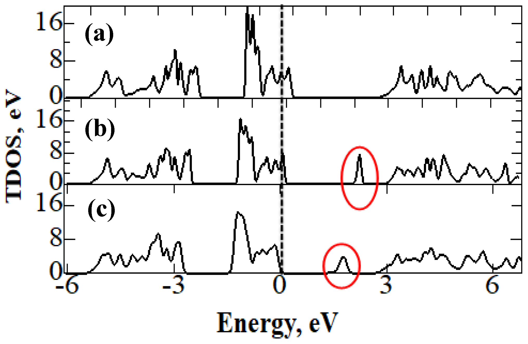
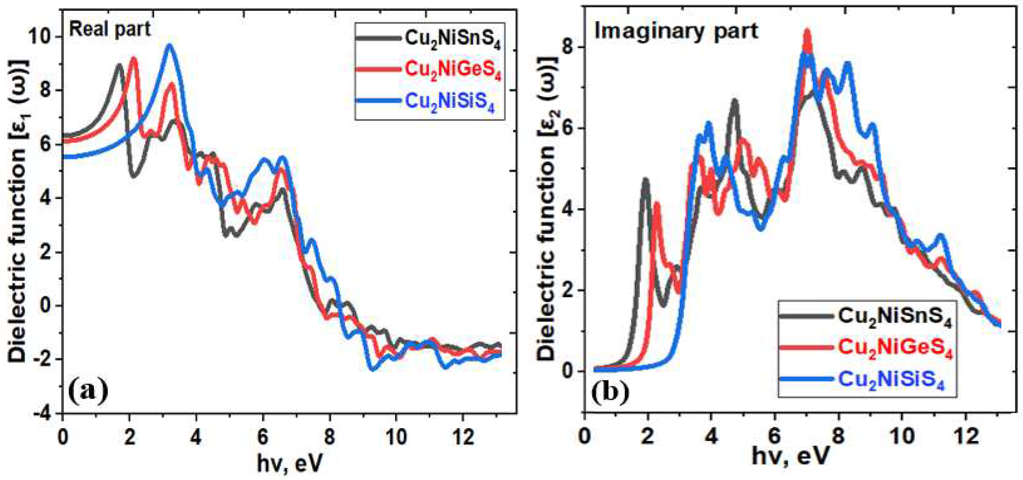
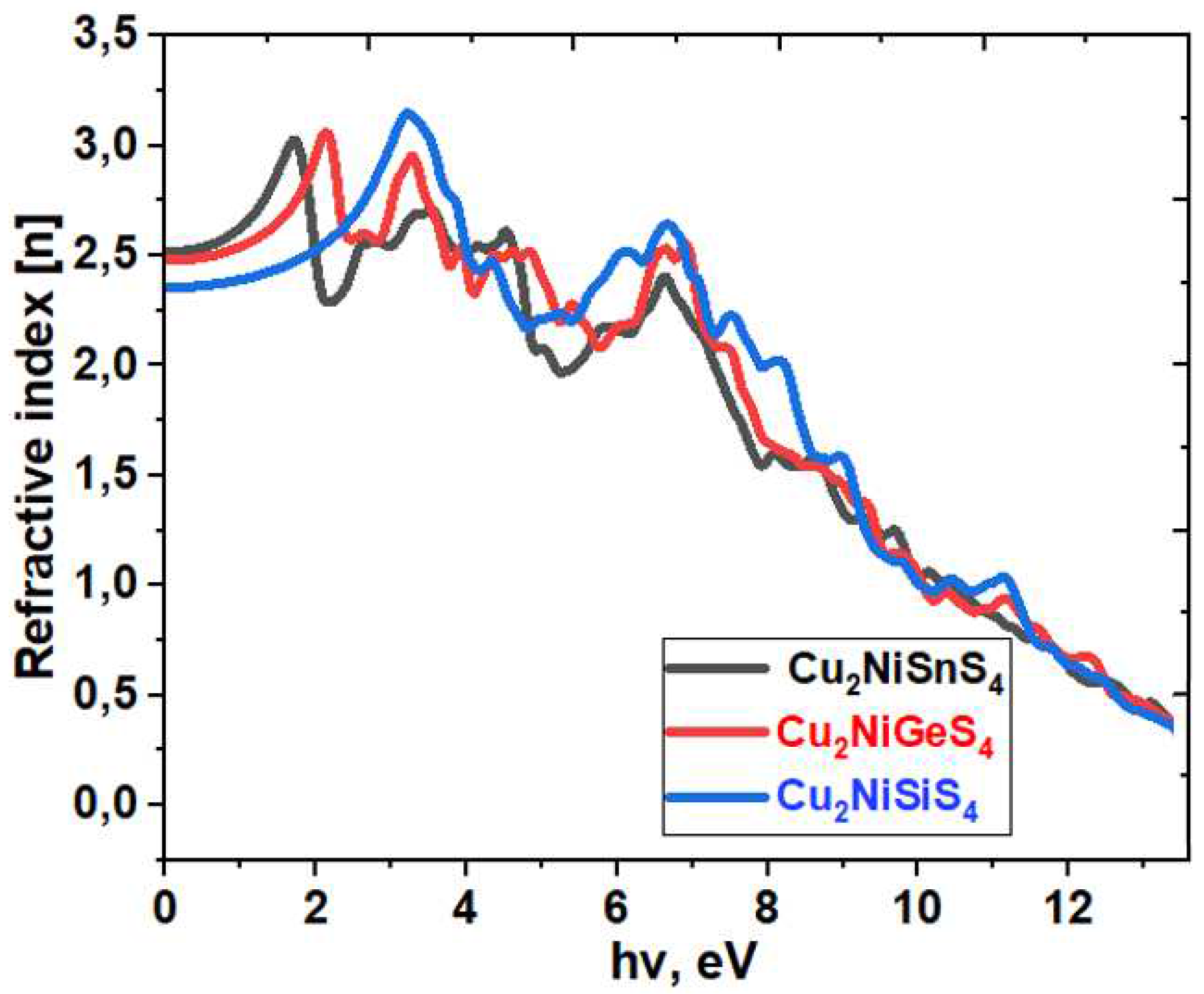
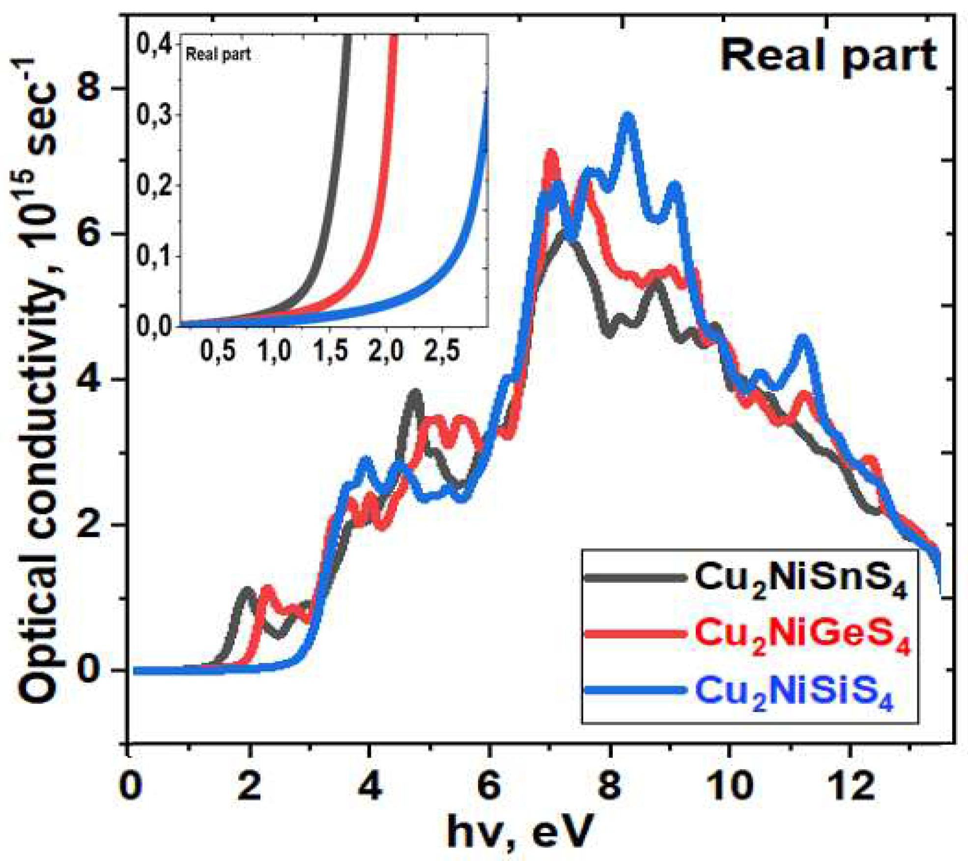
| Bandgap, eV | |||
|---|---|---|---|
| THIS WORK | LITERATURE | ||
| HSE06 | Calc. | Experimental | |
| Cu2NiSiS4 | 2.560 | - | - |
| Cu2NiGeS4 | 1.802 | 1.13 [53] | 1.8 [53] |
| Cu2NiSnS4 | 1.321 | 1.26 [54] | 1.31 [55], 1.38 [56] |
| System | ε1x(0) | ε2z(0) | n |
|---|---|---|---|
| Cu2NiSiS4 | 5.68 | 5.61 | 2.52 |
| Cu2NiGeS4 | 6.11 | 6.46 | 2.48 |
| Cu2NiXSnS4 | 6.46 | 6.88 | 2.36 |
Disclaimer/Publisher’s Note: The statements, opinions and data contained in all publications are solely those of the individual author(s) and contributor(s) and not of MDPI and/or the editor(s). MDPI and/or the editor(s) disclaim responsibility for any injury to people or property resulting from any ideas, methods, instructions or products referred to in the content. |
© 2024 by the authors. Licensee MDPI, Basel, Switzerland. This article is an open access article distributed under the terms and conditions of the Creative Commons Attribution (CC BY) license (http://creativecommons.org/licenses/by/4.0/).


