1. Introduction
Copper-nickel (Cu-Ni) alloys find widespread application in marine settings, including heat exchangers, piping, and valves. Their resistance to corrosion and bio-fouling makes them the preferred choice for highly corrosive environments [
1,
2,
3,
4], such as seawater, particularly when exceptional thermal conductivity is essential [
5,
6]. The 70/30 Cu-Ni alloy is mainly used in the critical parts with more demanding conditions. The Cu-Ni alloys primarily consist of α-phase-based single solid solutions due to the mutual solubility of Cu and Ni [
7]. Traditional manufacturing processes for Cu–Ni alloys involve casting and forging, which are time-consuming and expensive, especially when fabricating parts with intricate designs.
Consequently, there is a need for innovative methods that offer fast production and cost-effectiveness. Therefore, there has been a notable surge in the exploration of additive manufacturing (AM) methods, such as powder bed fusion, and direct energy deposition (DED) [
8,
9]. One significant drawback associated with metal powder-based AM techniques is their relatively low deposition rate, typically ranging from 0.12 to 0.6 kilograms per hour. In contrast, wire-arc DED or wire-arc additive manufacturing (WAAM), a high-deposition-rate technique that utilizes modified welding equipment, stands out for its low capital investment requirements and the ability to achieve deposition rates up to a hundred times higher. Consequently, it has emerged as a subject of immediate interest within the scientific and research community [
10,
11]. While several welding modes are suitable for WAAM, the cold metal transfer (CMT) method is favored due to its ability to lower heat input and enhance arc stability through the physical retraction of the wire, facilitating droplet detachment [
12].
However, the existing body of literature on additive manufacturing, in particular WAAM, using Cu–Ni raw materials is very limited [
13,
14]. In this study, the 70/30 Cu-Ni alloys are printed by WAAM using CMT method. The microstructures and defects of the as-build sample have been characterized as a variation of printing conditions. The corrosion properties have been investigated employing electrochemical approaches in sodium chloride solution.
2. Materials and Methods
2.1. Process Parameter Development
The machine used in this study is the Arc605 machine, manufactured by Gefertec (Berlin, Germany), a 5-axis CNC machine utilizing a Fronius TPS 400i power source from Wels, Austria. A 1.2 mm diameter 70-30 Cu-Ni wire from Lincoln Electric was employed for printing on a 70-30 Cu-Ni substrate. The chemical concentration of the wire is given as Cu-30.3 Ni-0.8Si (at %). The CMT power source from Fronius was utilized, and the shielding gas used was a mixture of 75% Ar and 25% He from Linde, flowing at a rate of 15 liters per minute. A pyrometer Metis M318 was used to keep the interpass temperature of the walls below 200 °C. The torch speed (TS) has been varied from 500 mm/min~1000 mm/min.
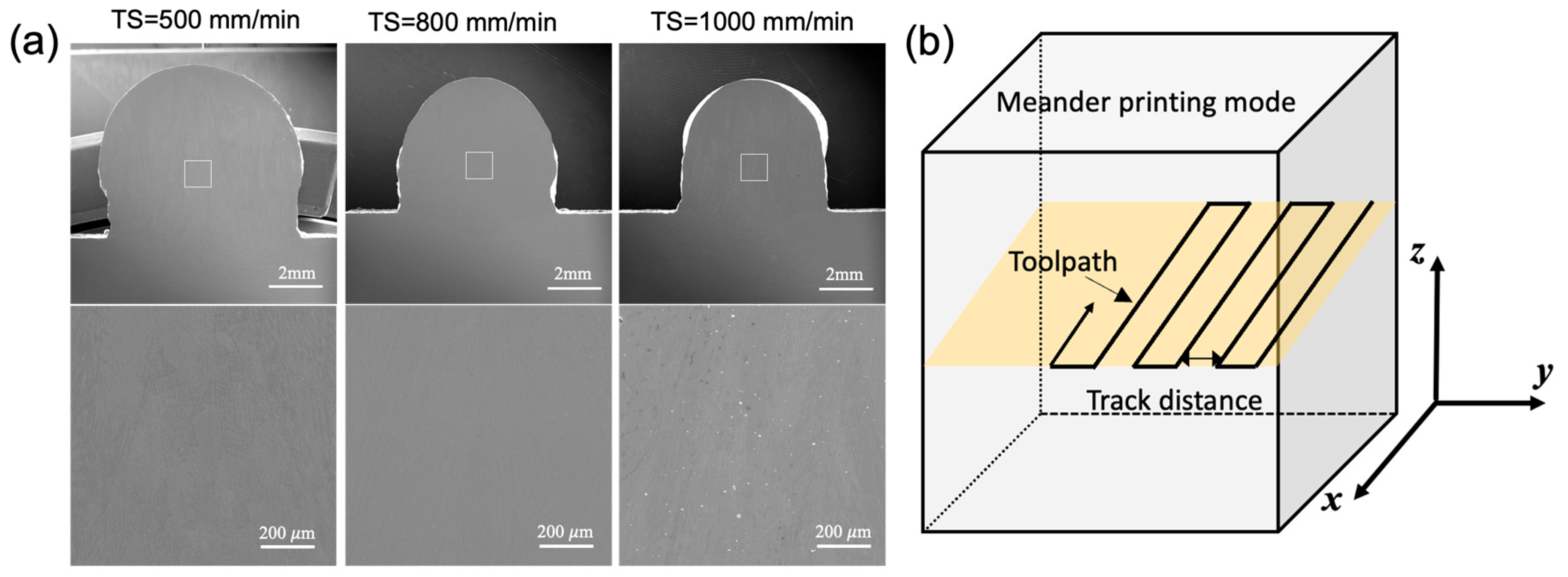
Initially, a single bead wall, 100 mm in length, was printed for 3 layers to screen the processing parameters (i.e., WFS and TS) in the medium-to-high production domain to ensure a high-quality build free of waviness and minimal other types of defects by scanning electron microscopy (
Figure 1a). Subsequently, the block was printed using a meander deposition path (
Figure 1b) based on the parameters that produced successful single bead walls, as listed in
Table 1, with variations in the track distance. The track distance was chosen as approximately 40% and 70% of the single-track width.
2.2. Microstructural Characterization, Corrosion and Mechanical Tests
The microstructures of the samples were assessed using optical microscopy (OM), scanning electron microscopy (SEM), Energy-Dispersive X-ray spectroscopy (EDS) and electron backscatter diffraction (EBSD). To prepare the samples for OM/SEM/EBSD analysis, they underwent mounting, grinding, and either vibration polishing or electropolishing. Electropolishing was carried out using a solution consisting of 12.5% sulfuric acid and 87.5% methanol at a potential of 25 V and room temperature. Etching was performed electrolytically in a 10% saturated oxalic acid solution at 12 V for a brief period. For samples intended for transmission electron microscope (TEM) analysis, preparation involved the use of a twin-jet polisher with a solution composed of 10 parts perchloric acid, 45 parts methanol, and 45 parts glacial acetic acid by volume, at 228 K and a potential of 15 V.
For electrochemical testing, the specimens were EDM machined from the build block in the size of 10×10×5 mm with the broad surface along the XY and YZ build plane. The sample are sealed with epoxy resin, exposing an area of 0.32 cm2 and ground to a P2400 grit finish. A three-electrode cell is used with a graphite counter electrode and the aqueous Ag/AgCl reference electrode as the reference point for all potentials. The test solution is a 3.5 wt.% (0.61 M) NaCl, and experiments are conducted at room temperature under natural aeration. The sample was immersed in the solution under the open circuit condition for 3 hours prior to the electrochemical impedance spectroscopy (EIS) and cyclic polarization (CP) tests. The sample after each electrochemical (either EIS or CP test) was ground to expose fresh surfaces. The EIS test was performed using a 10 mV (rms) perturbation from 100 kHz to 10 mHz. Fitting was performed with Gamry software. Cyclic polarization curves follow the forward scan rate of 0.1667 mV/s, starting from -250 mV (vs. open circuit potential). Reversal occurs when the current density reaches 3 mA/cm2 at a reverse scan rate of 1.667 mV/s. Electrochemical measurements are recorded using a Gamry potentiostat/galvanostat. The reported data represents the average of at least three measurements.
3. Results
3.1. Microstructural Analysis
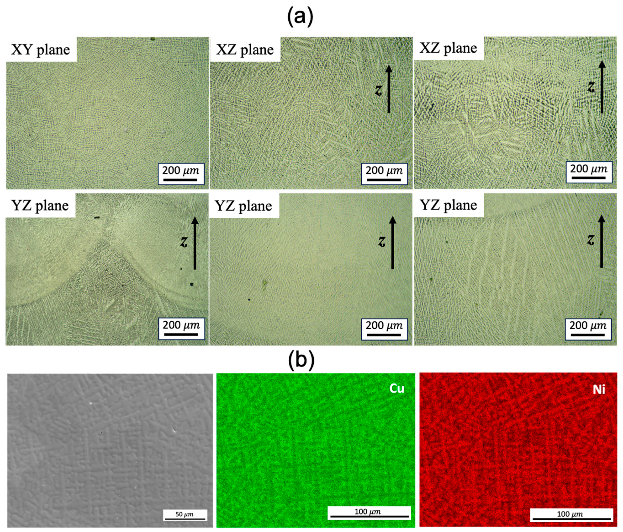
The microstructure examined by optical microscopy (OM) analysis reveals no porosity or macro/microscopic cracks (
Figure 2a). Dendrites are clearly observed, with the primary dendrite arm spacing (PDAS) varying in different locations, particularly adjacent to the fusion lines/melt pool boundaries. The dendrites mostly grow perpendicular to the melt pool boundaries (
Figure 2a). According to Hunt’s model [
15], the PDAS increases as the temperature gradient decreases. The heterogeneous PDAS indicates the presence of a complicated solidification environment. The energy-dispersive X-ray spectroscopy (EDS) analysis of the selected domain confirms the presence of solute segregation, with Ni elements preferentially locating in the dendrite cores compared to the inter-dendritic spacing (
Figure 2b). This aligns with the expectations based on the phase diagram of the Cu-Ni binary alloy. The formation of intermetallic compounds is not found, as Cu and Ni are completely soluble in each other as a single-phase solid solution.
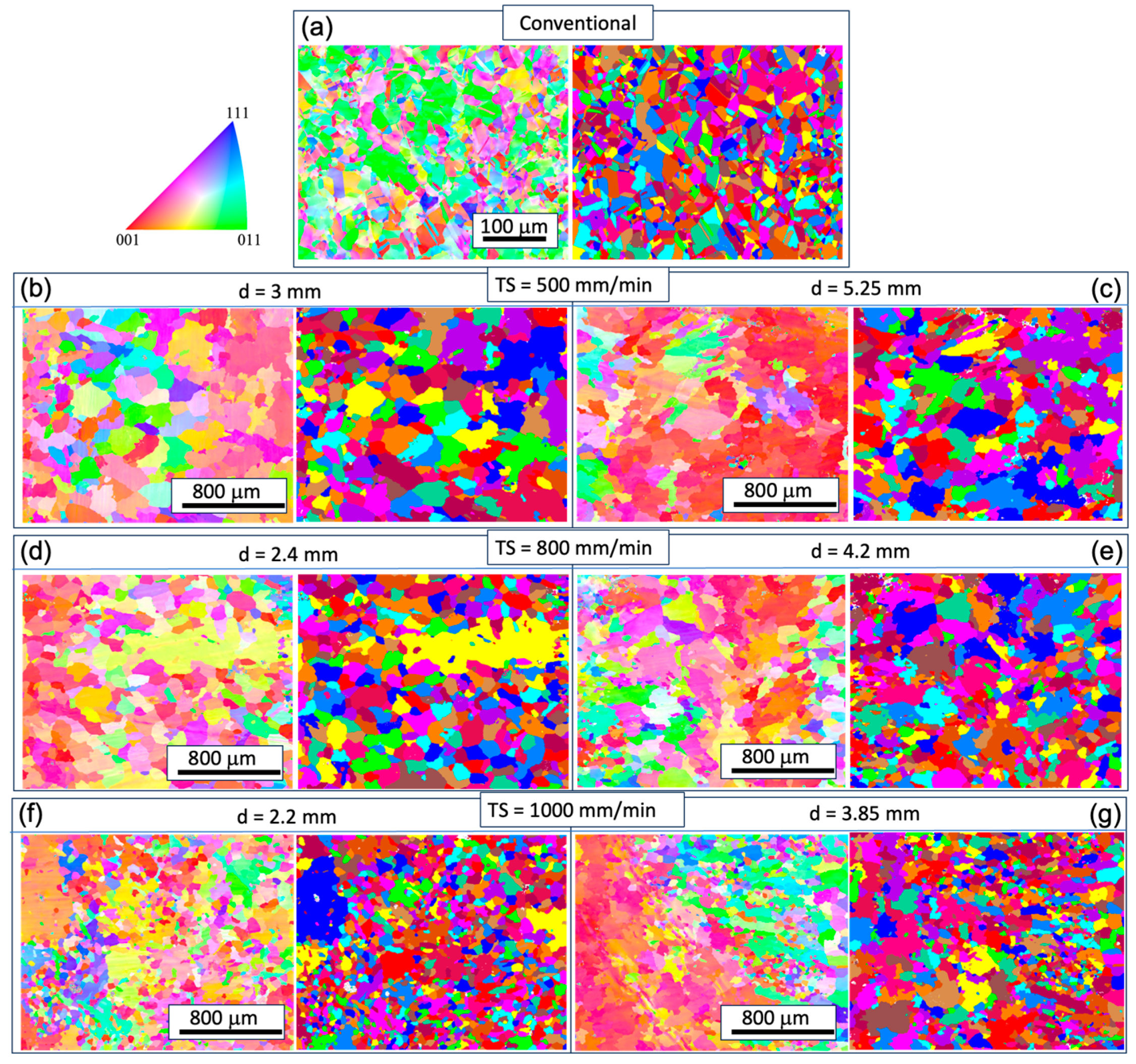
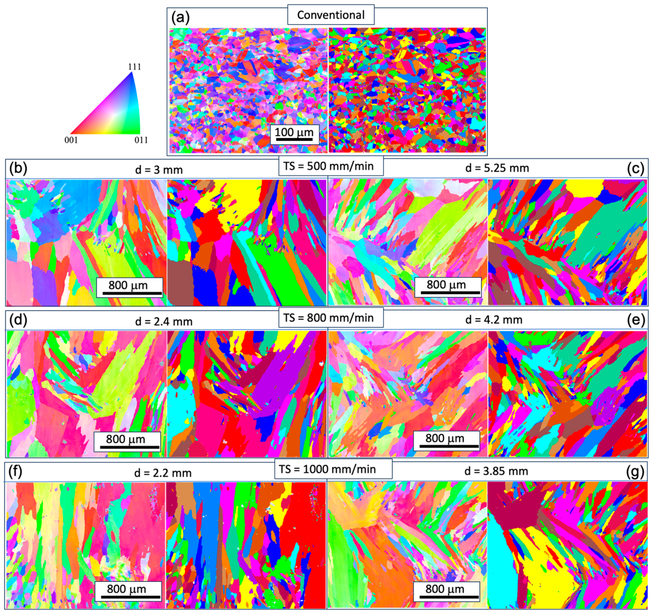
To understand the microstructural and texture changes that occur during the printing process, EBSD analyses were conducted for all the WAAM samples. For comparison, the analysis of the conventional sample is also presented. In
Figure 3 and
Figure 4, inverse pole figure maps (IPF) and contour pole figures (PF) on the XY-plane (perpendicular to the build direction) and YZ-plane (along the build direction) are provided. The XY cross-sections of the grains exhibit an equiaxed shape, while the YZ-plane cross-sections display a columnar shape. The longitudinal directions of the grains tend to deviate from the build direction (z-axis). Given that the layer thickness is estimated to be 2~3 mm (
Figure 1), the grains likely do not span multiple layers, in contrast to the observations in Inconel 718 [
16]. This phenomenon is potentially related to the heat flux direction and temperature gradient within the melt pool, which worths further analysis. Epitaxial growth from previous grains occurs at the melt pool boundary, but these grains do not seem to be in preferential crystal growth direction thus are mostly hindered in the growth process, as seen in
Figure 4.
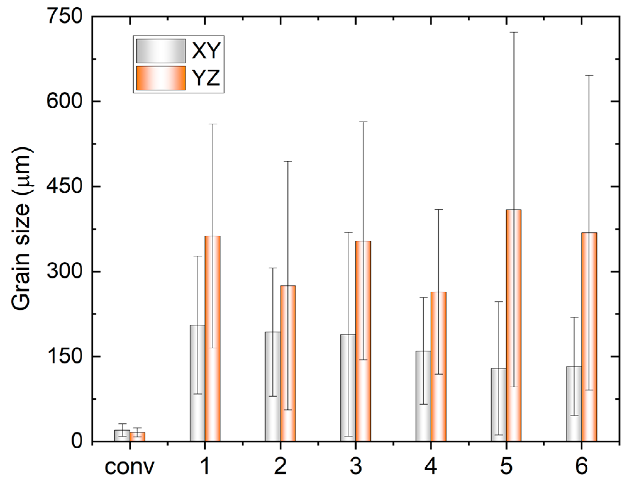
The grain size analysis in
Figure 5 reveals an increased aspect ratio of the columnar grains with rising TS, indicating smaller sizes in the XY-plane and larger sizes in the YZ-plane. Additionally, the size on the YZ-plane decreases with increasing track distance at the same WFS and TS, attributed to a faster cooling rate that benefits grain refinement. It is noteworthy that the very small grains in
Figure 3 and
Figure 4 may result from the intersection of some dendrite arms with the examined planes.
In contrast to the conventional condition, the predominance of red in the inverse pole figure (IPF) map signifies a concentration of the XY plane in the {001} texture (
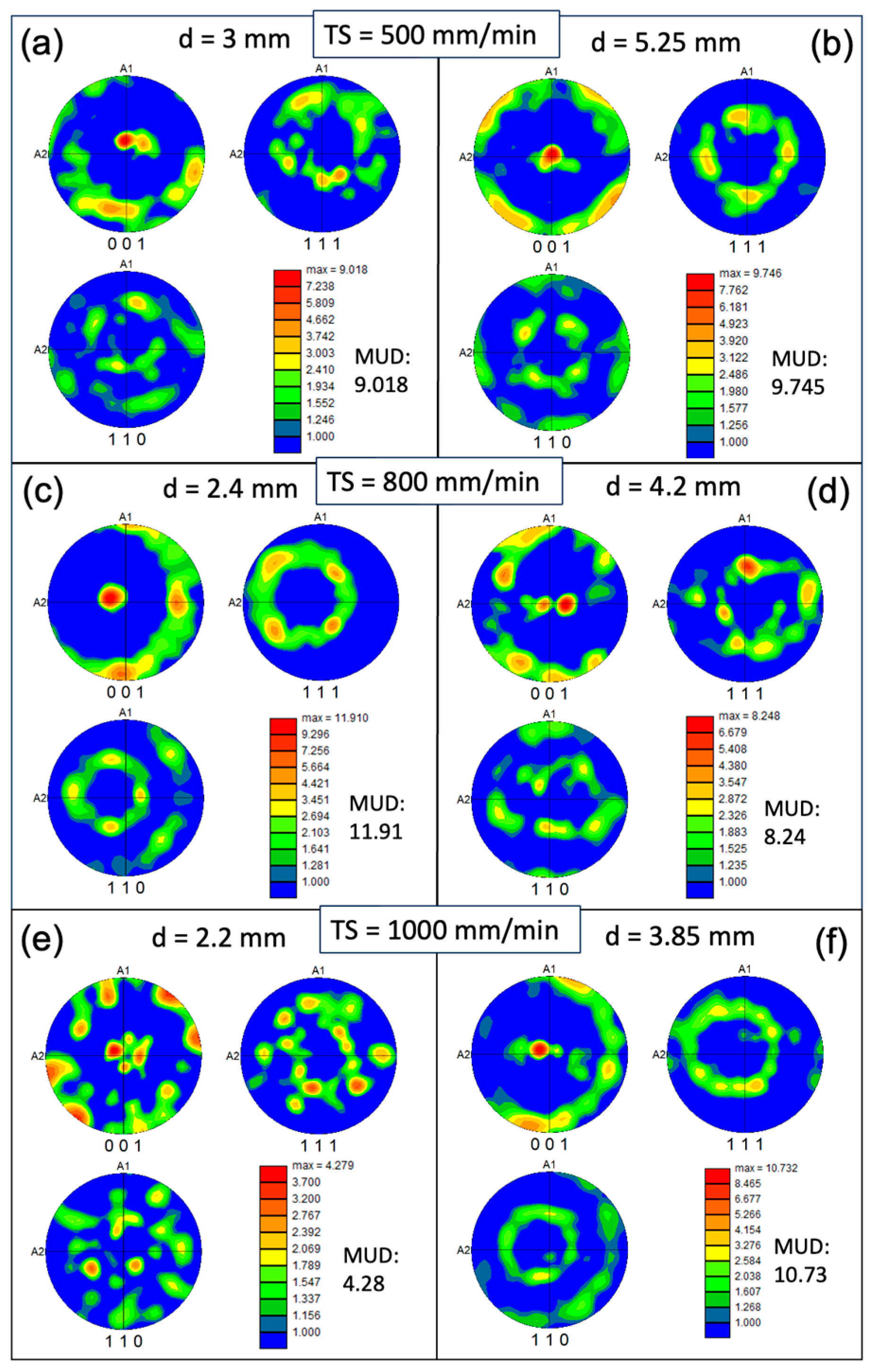
Figure 3). However, approximately 30-40% of the area in the XY cross-section consists of randomly oriented grains. The pole figure (PF) plots (
Figure 6) further illustrate the strength of the texture for the three families of planes in face-centered cubic (FCC) on {001}, {110}, and {111}. These plots confirm that the {001} texture component is the strongest among the three. The maximum multiple of uniform density (MUD) value is highest for sample 3 (MUD=11.9), even though the {001} is not strongly aligned along the z direction. Conversely, the MUD value is lowest for sample 5 (MUD=4.3), indicating a weak texture.
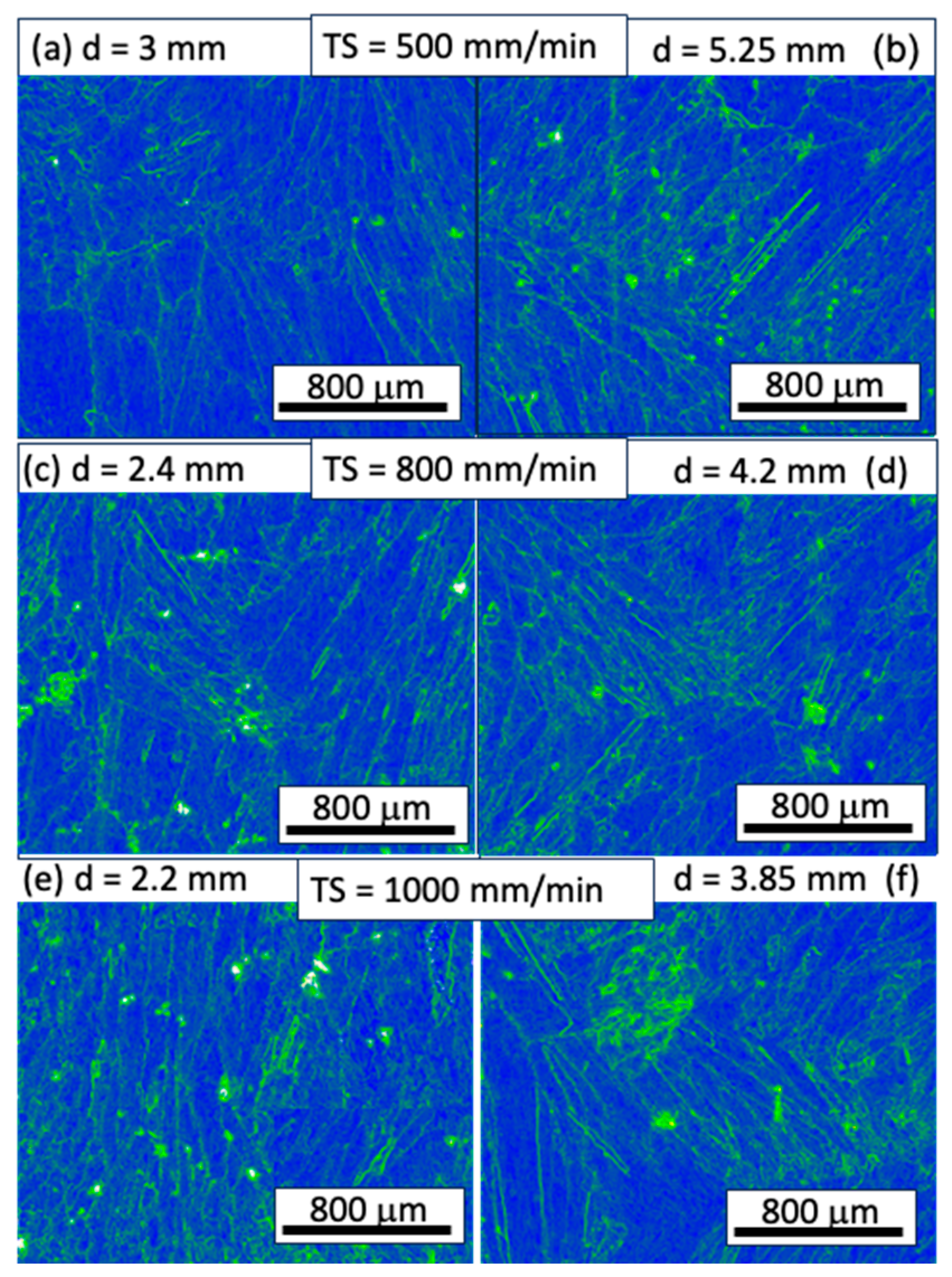
Figure 7 illustrates the kernel average misorientation (KAM) and grain boundaries of the EBSD analysis, presented for YZ planes. The KAM provides a qualitative description of the degree of homogenization of plastic deformation or the density of defects such as dislocations, lamellar dislocations, and subgrain boundaries. Higher KAM values indicate a greater degree of plastic deformation or a higher density of defects. The KAM analysis of the three samples reveals a low degree of dislocation in most regions, suggesting that residual stresses in the additively fabricated samples have been adequately released, and deformation within the grains is minimal. This phenomenon can be attributed to relatively slower cooling rate in WAAM process compared to other powder-based AM processes. Additionally, the stress-relieving annealing effect caused by the subsequent depositions may also be responsible.
3.2. Electrochemical Impedance Spectroscopy
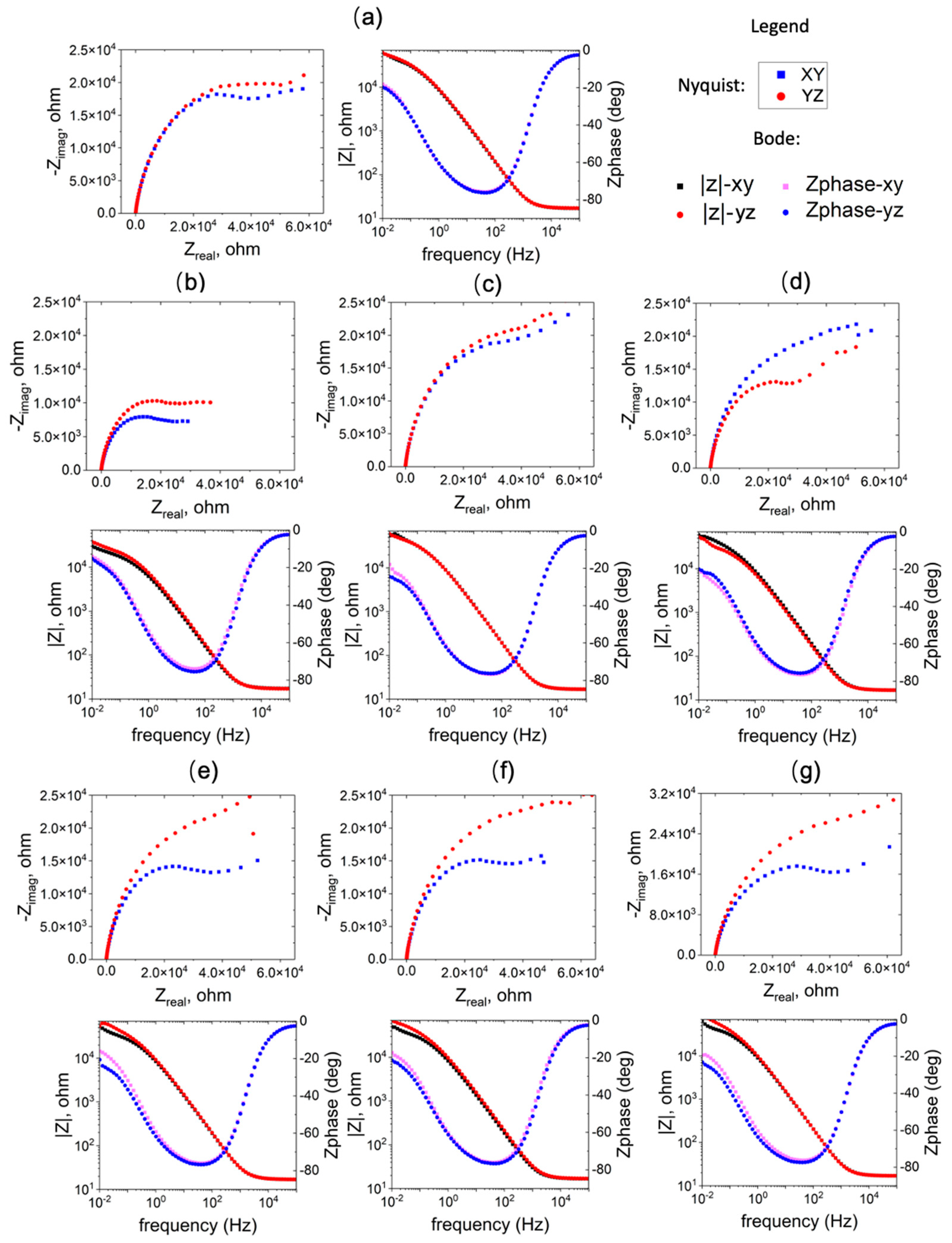
To investigate the corrosion resistance of the WAAM Cu/Ni, impedance spectra were recorded at the OCP, repeating the process 3-4 times for each sample.
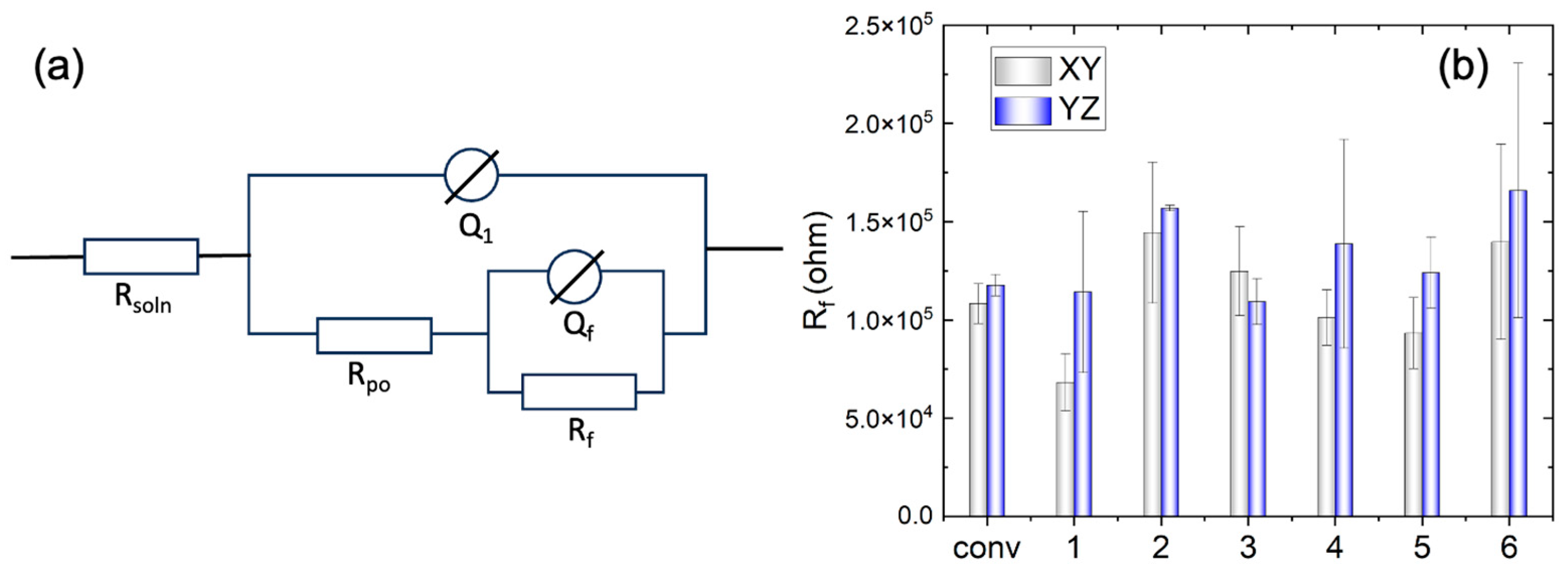
Figure 8 displays both Bode and Nyquist plots for the selected tests. The bode plot illustrates a consistent trend in impedance-frequency dependence across various conditions, with some discrepancies noted in the low-frequency domain (< 1Hz). In the Nyquist plot, the capacitive loop exhibits variable sizes based on processing conditions. Generally, a large semicircle suggests challenges in electron transfer between the substrate and solution. The high capacitance indicates a link between two processes: the formation of the passive oxide layer and the charging of the electric double layer. A secondary capacitive loop emerges at lower frequencies but displays some instability. The impedance spectra underwent analysis using the equivalent electrical circuit depicted in
Figure 9a. Here
Rsoln is the electrolyte resistance,
Rpo is the resistance inside the film pores,
Q1 the constant phase element (CPE) parallel to
Rpo.
Rf is the resistance of the corrosion product or film, and
Qf corresponds to the CPE parallel to
Rf. The use of a CPE is necessary due to a distribution of relaxation times resulting from heterogeneities at the electrode surface. The impedance of the CPE is given by
where
Q represents the impedance of the CPE,
n is the empirical exponent, which can vary between 1 for a perfect capacitor and 0 for a perfect resistor. The important fitting parameters are listed in
Table 2.
As can be seen in in
Figure 9b, the film resistance (R
f) of WAAM samples 2 and 6 surpasses that of the other conditions, exceeding that of the conventional sample. Conversely, sample 1 underperforms in comparison to the conventional ones. The elevated film resistance (R
f) suggests a deceleration in the kinetics of the electrochemical process. This behavior may be attributed to a higher growth rate of the passive film or an increased thickness of the passive layer. Additionally, the resistance on the YZ plane is higher than that on the XY plane for the WAAM samples, except for sample 3, where the horizontal (XY) and vertical (YZ) planes exhibit similar resistance (R
f).
Furthermore, the equivalent film thickness can be estimated from the fitted parameters from the EIS results with,
where
d is the film thickness,
is the vacuum permittivity (8.854×10
-12 F m
-1), ε is the dielectric constant, assumed as 7.11 which is the value for cuprous oxide Cu
2O, and
A is the effective surface area of the sample. The derivation of Eq. (2) is based on the equivalent film capacitance of the oxide layer that can be calculated with Eq. (3), which is then related to the equivalent film thickness via Eq. (4) [
17,
18],
The equivalent film thickness is thus calculated via Eq. (2), and the values are listed in
Table 2. The estimated surface film varies from tens to hundreds of nm.
3.3. ElectroPolarization Test
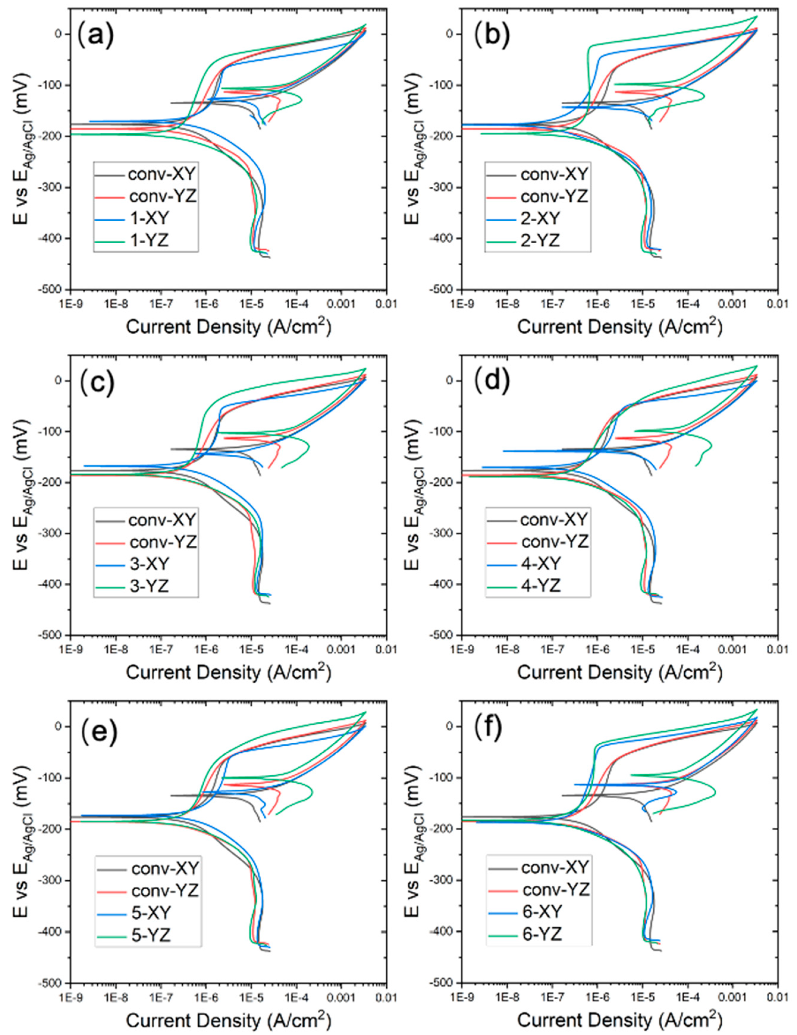
The cyclic potentiodynamic polarization curves, tested in the 3.5 wt% NaCl solution, are displayed in
Figure 10. The corrosion potential
Ecorr is summarized in
Figure 11a, where the difference between the conventional and WAAM samples is quite small. The YZ plane has a slightly more positive
Ecorr than that of the XY plane. As the potential shifts further in the positive direction, the quick current density increase is associated with transpassive dissolution. The potential at the current density of 5×10
-5 A cm
-2 is measured as the breakdown potential
Eb and summarized in
Figure 11b. Almost all the WAAM samples outperform the conventional one. WAAM sample 6 has the highest overall
Eb when considering both the XY and YZ plane. Moreover, the YZ plane has a higher
Eb than that of the XY plane. The YZ plane for sample 3 has the highest
Eb.
The conventional sample (depicted in black and red lines) demonstrate a domain of low current density domain (<5×10
-5 A cm
-2) before the transpassive dissolution. This can be ascribed to the protective corrosion product film formed on the sample surface. The passive region is atypical, as the passive current density (
ip) increases with a positively shifting applied potential. The passive current density over the potential window from -120 mV to -75 mV has been averaged and compared between the conventional and WAAM samples in
Figure 11c. WAAM sample 6 exhibits the lowest passive current density among them, significantly lower than that of the conventional one. WAAM sample 2 also demonstrates a slightly lower current density than the conventional one. Additionally, the passive current density is higher in the XY plane compared with that in the YZ plane. The YZ plane for sample 3 has the lowest
ip.
4. Discussion
The film resistance (Rf) measured by EIS, along with the Eb and ip measured by cyclic polarization tests, reveals differences in corrosion resistance, passivity, and transpassive behaviors between the conventional and WAAM Cu/Ni. WAAM sample 2 (TS=500 mm/min and track distance of 5.25 mm) and 6 (TS=1000 mm/min and track distance of 3.85 mm) exhibit higher film resistance (Rf) than the conventional sample in both XY and YZ build planes. Sample 6 also exhibits the lowest passive current density (ip) among the WAAM samples, significantly lower than that of the conventional one. WAAM sample 2 also demonstrates a slightly lower current density than the conventional one. In terms of breakdown potential Eb, almost all the WAAM samples outperform the conventional one. WAAM sample 6 has the highest overall Eb. Overall, the electrochemical analysis indicates that the WAAM sample 6 has the best corrosion performance in the 3.5% NaCl solution. Moreover, the YZ plane exhibits higher film resistance at OCP, higher transpassive potential, and lower passive current density compared to the XY plane, indicating better corrosion resistance.
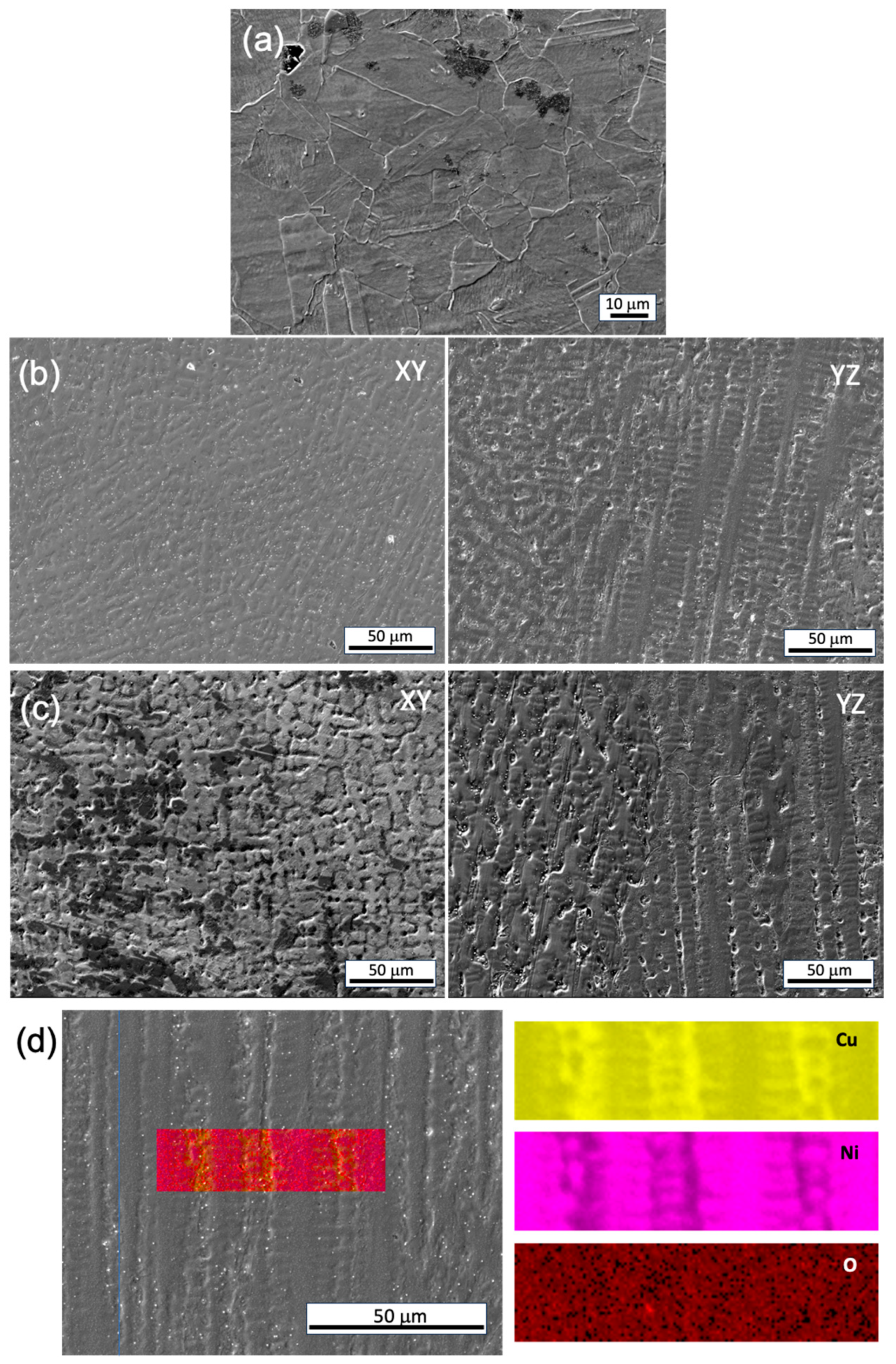
The corrosion morphologies of both the conventional and WAAM samples demonstrate uniform dissolution on the millimeter scale, but noteworthy differences in grain/subgrain level corrosion behavior exist. In the conventional sample, uneven corrosion depth is observed for grains with different orientations (
Figure 12a). In the WAAM sample, the inter-dendritic area is less resistant to corrosion attack compared to the dendritic core area (
Figure 12b,c), closely related to the uneven Ni element distribution as revealed in
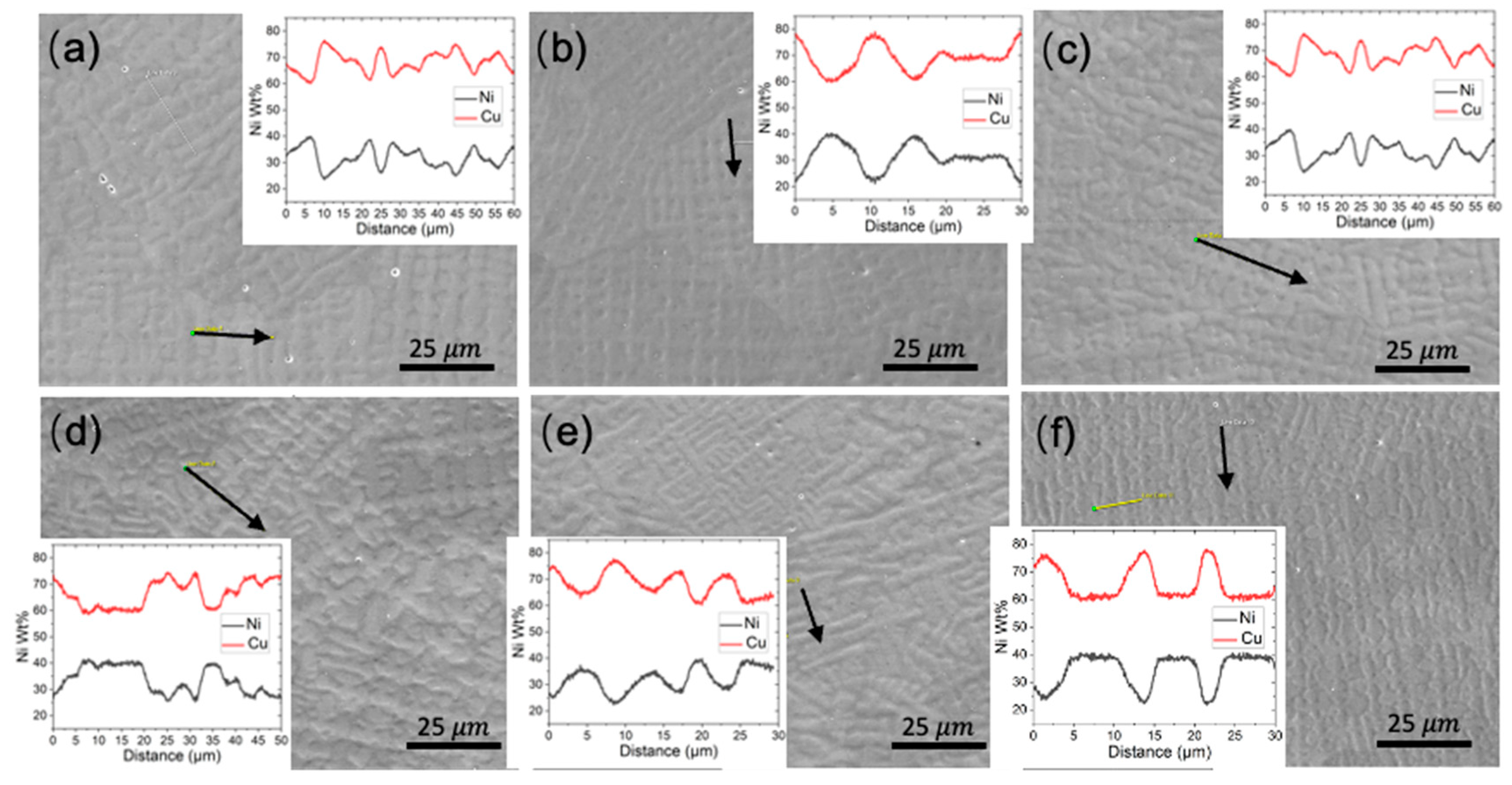
Figure 12d. A quantitative analysis using EDS line scan, as seen in
Figure 13, further reveals that the concentration difference between the dendritic core and inter-dendritic area can be as high as 20%. Due to the highly non-uniform distribution of Ni element at different locations, even for the same sample, making comparison among different printing conditions is not straightforward. The uneven Ni solute distribution could be ascribed to various factors: 1) The melt pool experiences a non-uniform cooling rate and temperature gradient. Typically, the bottom region undergoes a more rapid cooling rate and higher thermal gradient compared to the central molten pool. 2) Dendrite growth direction plays a crucial role in solute diffusion. Dendrites growing along the heat flux direction allow solute diffusion into the liquid away from the interface. Conversely, dendrites growing obliquely could be hindered by preceding dendrites. Furthermore, the solute concentration ahead of inclined dendrite tips surpasses that of dendrites perpendicular to the molten pool's isotherm [
19]. 3) Subsequent deposition leads to repetitive thermal cycling, potentially causing grain coarsening and migration of Ni solute driven by concentration gradients. However, due to Ni's slightly larger atomic radius compared to copper, the migration rate of atoms may become more challenging as the Ni content in the area increases. The increase of Ni element enhances the corrosion resistance, as the corrosion rate of Ni is at least two orders of magnitude lower than Cu [
20]. Ni could reside at the interface between the substrate/film interface or the inner side of the passive film [
21]. This Ni enrichment could occur quickly in the early stage when exposed to seawater [
21]. The contrast in corrosion resistance between the inter-dendritic and dendritic core areas is thus likely attributed to the depletion of Ni in the inter-dendritic area (
Figure 12).
It has been reported that the passive film formed on Cu-Ni alloy is different from that on stainless steels which is typically nanometer thick. The film on Cu-Ni takes a long time (several days to 2-3 months) at 15-17°C, with a thickness in micrometer [
21]. Additionally, its protection to the matrix is not as desirable when compared to that of stainless steels [
21]. The cuprous oxide (Cu
2O) film produced is believed to be predominately responsible for the corrosion protection, and the thicker passive film mainly reduces the corrosion rate by inhibiting the cathodic processes, such as the oxygen reduction reaction on the sample surface [
22]. In this work, the passive film formed during polarization test and that generated at OCP during the EIS test are formed within hours, may not be thick enough to inhibit the cathodic reaction by mitigating oxygen migration. However, it is still possible that the protective passive film is established within a few hours, as the associated discharge of copper ions can reduce tenfold during 10 min and 100-fold in the first hour [
23]. The estimated passive films from the EIS test listed in
Table 2 vary from tens to hundreds of nanometer. There could be inaccuracy in this estimate, that arise from the 1) the selection of the equivalent electric circuit and fitting process, 2) assuming the passive film as composed of cuprous oxide Cu
2O because the products of corrosion reactions could form a multi-layered oxide structure [
24]. Nevertheless, this thickness range is much smaller than the film formed for Cu-Ni alloy immersed in seawater for much longer time [
21], however the EIS test reveals a comparable film resistance as those exposed to much longer time [
22], indicating the film forming on 70/30 Cu-Ni within hours can possess substantial protectiveness.
5. Conclusions
In this study, the 70/30 Cu-Ni has been successfully fabricated by WAAM at the TS varied from 500 mm/min to 800 mm/min. A conventional 70/30 Cu-Ni was also investigated as comparison purposes. The as-built microstructures of WAAM Cu-Ni were analyzed, considering the grain structure, chemical segregation, along with other defects. Corrosion properties were examined in a 3.5 wt% NaCl solution. The main conclusions are drawn as follows:
The as-fabricated microstructures are characterized by columnar grains with prominent dendrites. The longitudinal direction of the columnar grain deviates from the build direction. Strong chemical segregation has been observed in the form of Ni element depletion in the inter-dendritic area.
With increasing TS, the aspect ratio of columnar grains increases, resulting in a reduced size of the XY cross-section and an increased length of the YZ cross-section. The grain size also decreases with increasing track distance. A close-to-{001} texture has developed on 30% to 40% of the area on the XY plane. The grain size of the conventional sample is one order of magnitude smaller compared with that of the WAAM ones, and exhibits random orientation.
The corrosion performance is evaluated in terms of film resistance at OCP, the passive current density and breakdown potential during polarization. Two WAAM samples, produced under a TS of 800 mm/min and track distance of 5.25 mm as well as a TS of 1000 mm/min and track distance of 3.85 mm, have the best corrosion performance in the 3.5% NaCl solution.
Anisotropy in the corrosion performance has also been observed. The YZ plane exhibits higher film resistance at OCP, a higher breakdown potential, and lower passive current density, compared to the XY plane, indicating better corrosion resistance.
At the grain/subgrain level, the conventional Cu-Ni demonstrates crystallography-dependent corrosion resistance, whereas the WAAM Cu-Ni exhibits preferential corrosion attack at the inter-dendritic area due to the uneven distribution of Ni element. The reason behind the apparent corrosion enhancement in the aforementioned WAAM Cu-Ni samples compared to its conventional counterpart need further analysis, which will be carried out in our study in the near future.
This study aims to provide a microstructural and corrosion analysis of the WAAM Cu-Ni processed by various printing parameters. It paves the way to further understand the applicability of WAAM to copper-based alloys and optimize their corrosion properties though tailored microstructures by optimizing the printing parameters and post-processing methods.
Author Contributions
Conceptualization, J.S. and Y.F.; methodology, J.S., X.J., A.T. and Y.F.; formal analysis, J.S., X.J. and Y.F.; investigation, J.S., X.J. and Y.F.; resources, A.T. and Y.F.; data curation, J.S. and X.J.; writing—original draft preparation, J.S. and X.J.; writing—review and editing, J.S., X.J., A.T. and Y.F.; visualization, J.S. and X.J.; supervision, A.T. and Y.F.; project administration, Y.F.; funding acquisition, Y.F. All authors have read and agreed to the published version of the manuscript.
Funding
This research was funded by Office of Naval Research, grant number N00014-21-1-2800.
Data Availability Statement
The data presented in this study are available on request from the corresponding author.
Acknowledgments
This work utilized the Nanoscale Characterization and Fabrication Laboratory, a part of the National Nanotechnology Coordinated Infrastructure (NNCI), funded by NSF (ECCS 1542100 and ECCS 2025151).
Conflicts of Interest
The authors declare no conflict of interest.
References
- Zhu, X.; Lei, T. Characteristics and formation of corrosion product films of 70Cu–30Ni alloy in seawater. Corrosion Science 2002, 44, 67–79. [Google Scholar] [CrossRef]
- Wang, Y.Z.; Beccaria, A.M.; Poggi, G. The effect of temperature on the corrosion behaviour of a 70/30 Cu-Ni commercial alloy in seawater. Corrosion Science 1994, 36, 1277–1288. [Google Scholar] [CrossRef]
- Chauhan, P.K.; Gadiyar, H.S. An XPS study of the corrosion of Cu-10 Ni alloy in unpolluted and polluted sea-water; the effect of FeSO4 addition. Corrosion Science 1985, 25, 55–68. [Google Scholar] [CrossRef]
- Mansfeld, F.; Little, B. Microbiologically influenced corrosion of copper-based materials exposed to natural seawater. Electrochimica Acta 1992, 37, 2291–2297. [Google Scholar] [CrossRef]
- Mao, X.; Fang, F.; Jiang, J.; Tan, R. Effect of rare earths on corrosion resistance of Cu-30Ni alloys in simulated seawater. Journal of Rare Earths 2009, 27, 1037–1041. [Google Scholar] [CrossRef]
- Martin, J.R.; Heidersbach, R.H.; Lenard, D.R. Dealloying of cupronickels in stagnant seawater in Proceedings of NACE International, Houston, TX, USA, 1999.
- Lee, W.-H.; Chung, K.C. Investigation of a copper–nickel alloy resistor using co-electrodeposition. Journal of Applied Electrochemistry 2020, 50, 535–547. [Google Scholar] [CrossRef]
- Armstrong, M.; Mehrabi, H.; Naveed, N. An overview of modern metal additive manufacturing technology. Journal of Manufacturing Processes 2022, 84, 1001–1029. [Google Scholar] [CrossRef]
- Durai Murugan, P.; Vijayananth, S.; Natarajan, M.P.; Jayabalakrishnan, D.; Arul, K.; Jayaseelan, V.; Elanchezhian, J. A current state of metal additive manufacturing methods: A review. Materials Today: Proceedings 2022, 59, 1277–1283. [Google Scholar] [CrossRef]
- Shah, A.; Aliyev, R.; Zeidler, H.; Krinke, S. A Review of the Recent Developments and Challenges in Wire Arc Additive Manufacturing (WAAM) Process. Journal of Manufacturing and Materials Processing 2023, 7. [Google Scholar] [CrossRef]
- Kumar, N.; Bhavsar, H.; Mahesh, P.V.S.; Srivastava, A.K.; Bora, B.J.; Saxena, A.; Dixit, A.R. Wire Arc Additive Manufacturing – A revolutionary method in additive manufacturing. Materials Chemistry and Physics 2022, 285, 126144. [Google Scholar] [CrossRef]
- Rodrigues, T.A.; Duarte, V.; Miranda, R.M.; Santos, T.G.; Oliveira, J.P. Current Status and Perspectives on Wire and Arc Additive Manufacturing (WAAM). Materials 2019, 12. [Google Scholar] [CrossRef]
- Guo, C.; Kang, T.; Wu, S.; Ying, M.; Liu, W.M.; Chen, F. Microstructure, mechanical, and corrosion resistance of copper nickel alloy fabricated by wire-arc additive manufacturing. MRS Communications 2021, 11, 910–916. [Google Scholar] [CrossRef]
- Miao, Y.; Li, C.; Zhao, Y.; Wu, Y.; Liu, J.; Wang, Z.; Zhang, B. Material Properties of Functionally Gradient Copper-Nickel Alloy Fabricated by Wire Arc Additive Manufacturing Based on Bypass-Current Paw. 2023. [Google Scholar] [CrossRef]
- Hunt, J.D.; Lu, S.Z. Numerical modeling of cellular/dendritic array growth: spacing and structure predictions. Metallurgical and Materials Transactions A 1996, 27, 611–623. [Google Scholar] [CrossRef]
- Song, J.; Jimenez, X.A.; Russell, C.; To, A.C.; Fu, Y. Unusually high room and elevated-temperature tensile properties observed in direct aged wire-arc directed energy deposited Inconel 718. Scientific Reports 2023, 13, 19235. [Google Scholar] [CrossRef] [PubMed]
- Hsu, C.H.; Mansfeld, F. Technical Note: Concerning the Conversion of the Constant Phase Element Parameter Y0 into a Capacitance. Corrosion 2001, 57, 747–748. [Google Scholar] [CrossRef]
- Mansfeld, F. Electrochemical impedance spectroscopy (EIS) as a new tool for investigating methods of corrosion protection. Electrochimica Acta 1990, 35, 1533–1544. [Google Scholar] [CrossRef]
- Geng, R.; Cheng, Y.; Chao, L.; Wei, Z.; Ma, N. Microstructure and Solute Concentration Analysis of Epitaxial Growth during Wire and Arc Additive Manufacturing of Aluminum Alloy. Crystals 2023, 13. [Google Scholar] [CrossRef]
- EFIRD, K.D. Potential-pH Diagrams for 90-10 and 70-30 Cu-Ni in Sea Water. Corrosion 2013, 31, 77–83. [Google Scholar] [CrossRef]
- Ma, A.L.; Jiang, S.L.; Zheng, Y.G.; Ke, W. Corrosion product film formed on the 90/10 copper–nickel tube in natural seawater: Composition/structure and formation mechanism. Corrosion Science 2015, 91, 245–261. [Google Scholar] [CrossRef]
- Wu, L.; Ma, A.; Zhang, L.; Li, G.; Hu, L.; Wang, Z.; Zheng, Y. Erosion–Corrosion Behavior of 90/10 and 70/30 Copper–Nickel Tubes in 1 wt% NaCl Solution. Metals 2023, 13. [Google Scholar] [CrossRef]
- Tuthill, A.H. Guidelines for the Use of Copper Alloys in Seawater. NiDI Publication 1988, 12003. [Google Scholar]
- Schleich, W. Application of Copper-Nickel Alloy UNS C70600 for Seawater Service in Proceedings of CORROSION 2005, Houston, Texas, 2005.
Figure 1.
(a) SEM image of (upper panel) cross-section of the single-bead 3-layer build and (lower panel) magnified SEM image of selected area in the upper panel (indicated by white box); the three columns correspond to the TS equal to 500, 800, and 1000 mm/min; (b) schematic of the deposition strategy.
Figure 2.
(a) OM images of the dendrite feature on different build planes and (b) SEM image and EDS map scanning of the WAAM sample 1.
Figure 2.
(a) OM images of the dendrite feature on different build planes and (b) SEM image and EDS map scanning of the WAAM sample 1.
Figure 3.
Inverse pole figure (IPF) (left) and grain structure (right) maps on the XY plane at different track distance (d) with respective torch speed (TS) as follows: TS=500 mm/min, 800 mm/min, and 1000 mm/min; subfigure (b–g) correspond to WAAM sample 1-6.
Figure 3.
Inverse pole figure (IPF) (left) and grain structure (right) maps on the XY plane at different track distance (d) with respective torch speed (TS) as follows: TS=500 mm/min, 800 mm/min, and 1000 mm/min; subfigure (b–g) correspond to WAAM sample 1-6.
Figure 4.
Inverse pole figure (IPF) (left) and grain structure (right) maps on the YZ plane at different track distance (d) with respective torch speed (TS) as follows: TS=500 mm/min, 800 mm/min, and 1000 mm/min; subfigure (b–g) correspond to WAAM sample 1-6.
Figure 4.
Inverse pole figure (IPF) (left) and grain structure (right) maps on the YZ plane at different track distance (d) with respective torch speed (TS) as follows: TS=500 mm/min, 800 mm/min, and 1000 mm/min; subfigure (b–g) correspond to WAAM sample 1-6.
Figure 5.
Variation of grain size in XY and YZ plane of the conventional sample (conv) and WAAM samples under the different printing conditions; x-axis label ‘1’-‘6’ indicate the WAAM sample 1-6.
Figure 5.
Variation of grain size in XY and YZ plane of the conventional sample (conv) and WAAM samples under the different printing conditions; x-axis label ‘1’-‘6’ indicate the WAAM sample 1-6.
Figure 6.
Pole figure (PF) colored orientation maps measured on the XY plane of the WAAM samples at different track distance (d) with respective torch speed (TS) as following: TS=500 mm/min, 800 mm/min, and 1000 mm/min; subfigure (a–f) correspond to WAAM sample 1-6.
Figure 6.
Pole figure (PF) colored orientation maps measured on the XY plane of the WAAM samples at different track distance (d) with respective torch speed (TS) as following: TS=500 mm/min, 800 mm/min, and 1000 mm/min; subfigure (a–f) correspond to WAAM sample 1-6.
Figure 7.
Kernel average misorientation (KAM) maps of WAAM samples at different travel speed (TS) of the YZ plane with respective TS as following: TS=500 mm/min, 800 mm/min, and 1000 mm/min; subfigure (a–f) correspond to WAAM sample 1-6.
Figure 7.
Kernel average misorientation (KAM) maps of WAAM samples at different travel speed (TS) of the YZ plane with respective TS as following: TS=500 mm/min, 800 mm/min, and 1000 mm/min; subfigure (a–f) correspond to WAAM sample 1-6.
Figure 8.
EIS results of the WAAM samples on the YZ plane; subfigure (a)-(f) correspond to WAAM sample 1-6.
Figure 8.
EIS results of the WAAM samples on the YZ plane; subfigure (a)-(f) correspond to WAAM sample 1-6.
Figure 9.
(a) Equivalent electrical circuit used to fit the impedance spectra, and (b) the fitted parameter Rf of the conventional sample (conv) and WAAM samples under the different printing conditions; x-axis label ‘1’-‘6’ indicate the WAAM sample 1-6.
Figure 9.
(a) Equivalent electrical circuit used to fit the impedance spectra, and (b) the fitted parameter Rf of the conventional sample (conv) and WAAM samples under the different printing conditions; x-axis label ‘1’-‘6’ indicate the WAAM sample 1-6.
Figure 10.
Potentiodynamic curve of WAAM samples: subfigure (a–f) correspond to WAAM sample 1-6; the conventional sample is presented in each subfigure as comparison.
Figure 10.
Potentiodynamic curve of WAAM samples: subfigure (a–f) correspond to WAAM sample 1-6; the conventional sample is presented in each subfigure as comparison.
Figure 11.
Extracted corrosion characteristics (a) corrosion potential, (b) breakdown potential, and (c) passive current density from the potentiodynamic test for conventional sample (conv) and WAAM samples under the different printing conditions; x-axis label ‘1’-‘6’ indicate the WAAM sample 1-6.
Figure 11.
Extracted corrosion characteristics (a) corrosion potential, (b) breakdown potential, and (c) passive current density from the potentiodynamic test for conventional sample (conv) and WAAM samples under the different printing conditions; x-axis label ‘1’-‘6’ indicate the WAAM sample 1-6.
Figure 12.
SEM image of the corrosion morphology post-potentiodynamic test: (a) conventional sample, (b) WAAM sample 4, (c) WAAM sample 6, (d) EDS area scan of the WAAM sample 6.
Figure 12.
SEM image of the corrosion morphology post-potentiodynamic test: (a) conventional sample, (b) WAAM sample 4, (c) WAAM sample 6, (d) EDS area scan of the WAAM sample 6.
Figure 13.
SEM images of the dendritic feature on the XY plane; arrow represents the EDS line scan and the results are the subfigure inset. Subfigure (a–f) correspond to WAAM sample 1-6.
Figure 13.
SEM images of the dendritic feature on the XY plane; arrow represents the EDS line scan and the results are the subfigure inset. Subfigure (a–f) correspond to WAAM sample 1-6.
Table 1.
Process parameter used to print 70-30 Cu-Ni single tracks.
Table 1.
Process parameter used to print 70-30 Cu-Ni single tracks.
| Specimen |
WFS |
TS |
Track Distance |
Interpass Temp (°C) |
| 1 |
8 m/min |
500 mm/min |
3 mm |
150~200 |
| 2 |
5.25 mm |
| 3 |
800 mm/min |
2.4 mm |
| 4 |
4.2 mm |
| 5 |
1000 mm/min |
2.2 mm |
| 6 |
3.85 mm |
Table 2.
Summary of the essential fitting parameters for the EIS results.
Table 2.
Summary of the essential fitting parameters for the EIS results.
| Specimen |
Rf × 105 (Ω) |
Qf × 10-5 (F) |
nf
|
df (μm) |
| XY |
YZ |
XY |
YZ |
XY |
YZ |
XY |
YZ |
| Wrought |
1.08 |
1.18 |
2.44 |
2.37 |
0.34 |
0.32 |
0.13 |
0.095 |
| 1 |
0.68 |
1.14 |
2.84 |
2.83 |
0.340 |
0.29 |
0.20 |
0.041 |
| 2 |
1.44 |
1.57 |
2.13 |
2.29 |
0.29 |
0.31 |
0.063 |
0.051 |
| 3 |
1.25 |
1.09 |
2.54 |
2.98 |
0.29 |
0.31 |
0.046 |
0.049 |
| 4 |
1.01 |
1.39 |
2.36 |
2.34 |
0.31 |
0.30 |
0.12 |
0.058 |
| 5 |
0.93 |
1.24 |
2.43 |
2.04 |
0.32 |
0.33 |
0.14 |
0.14 |
| 6 |
1.40 |
1.66 |
2.68 |
2.47 |
0.27 |
0.28 |
0.021 |
0.023 |
|
Disclaimer/Publisher’s Note: The statements, opinions and data contained in all publications are solely those of the individual author(s) and contributor(s) and not of MDPI and/or the editor(s). MDPI and/or the editor(s) disclaim responsibility for any injury to people or property resulting from any ideas, methods, instructions or products referred to in the content. |
© 2024 by the authors. Licensee MDPI, Basel, Switzerland. This article is an open access article distributed under the terms and conditions of the Creative Commons Attribution (CC BY) license (http://creativecommons.org/licenses/by/4.0/).
