Submitted:
24 January 2024
Posted:
25 January 2024
You are already at the latest version
Abstract
Keywords:
Introduction
MATERIALS AND METHODS
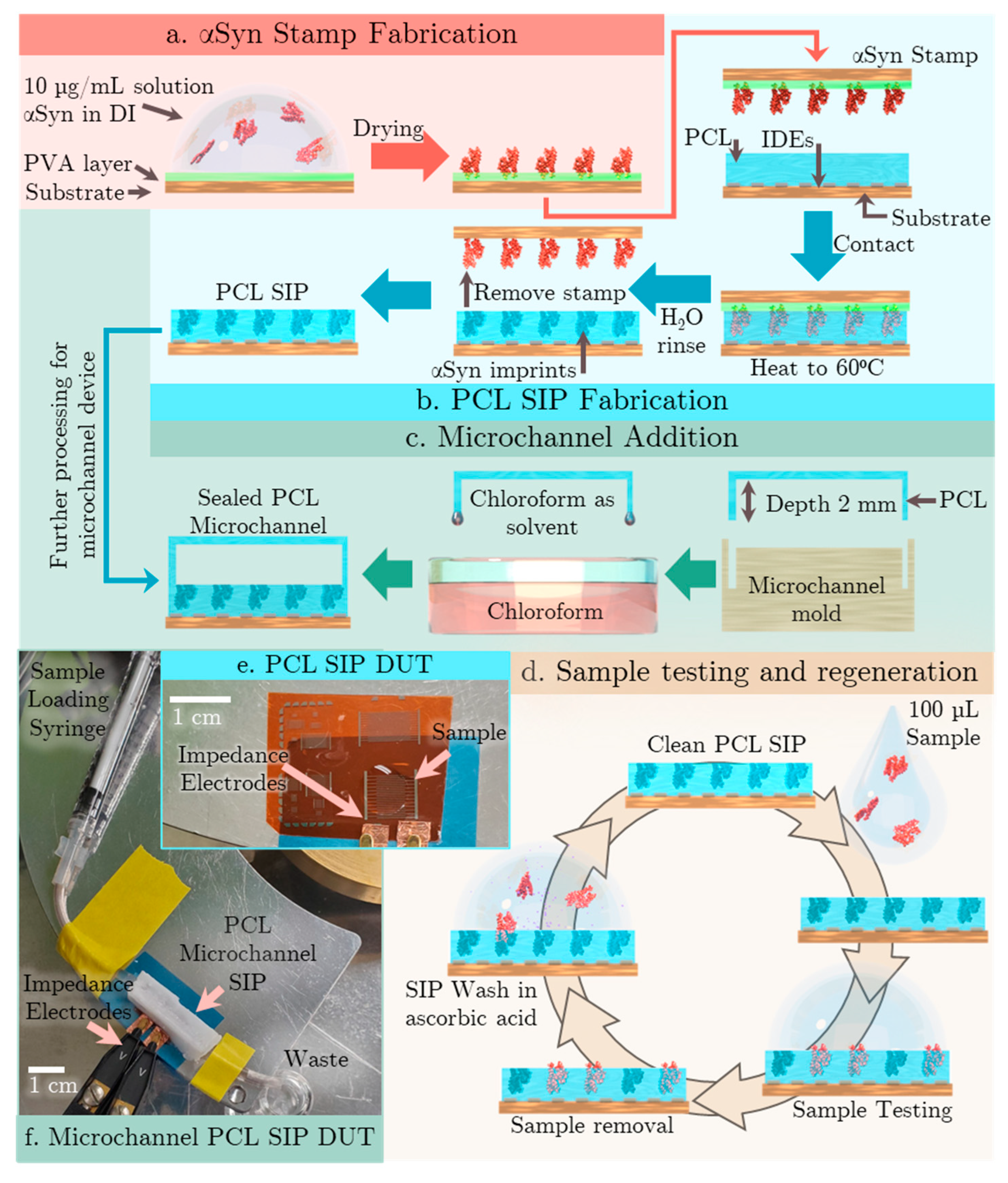
2.1. Device Fabrication
2.2. Sample Preparation
2.3. Testing Processes
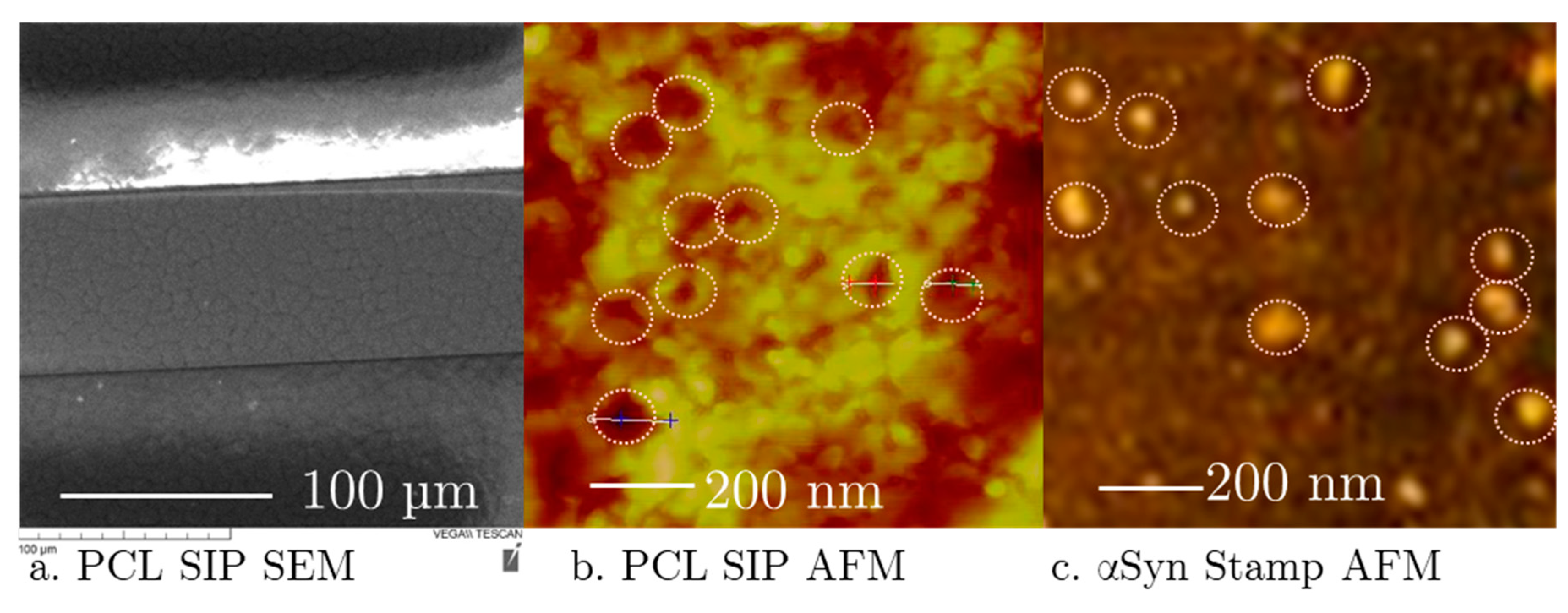
2.4. Atomic Force Microscopy of Soft-Printed SIP Surface
RESULTS AND DISCUSSION
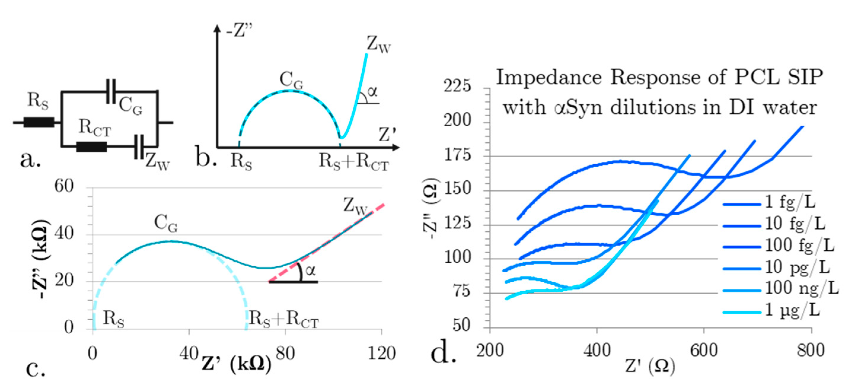
3.1. Impedance Spectroscopy Data Analysis
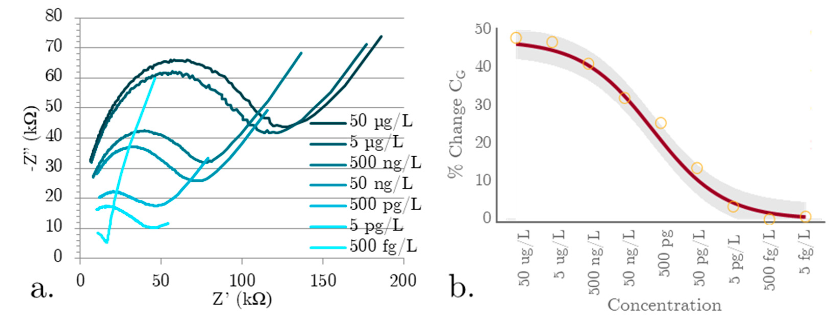
3.2. Characterizing Sensor Performance in
3.3. Preliminary Data from Microfluidic Channel SIP EIS Biosensor
Conclusions
Author Contributions
Funding
Acknowledgments
Conflicts of Interest
References
- E. Beghi et al. ‘Articles The burden of neurological diseases in Europe: an analysis for the Global Burden of Disease Study 2017’, Lancet Public Health, vol. 5, pp. 551–67, 2020, Accessed: Nov. 17, 2023. [Online]. Available: www.thelancet.com/.
- ‘Global action plan on the public health response to dementia’, Geneva, 2017. Accessed: Nov. 17, 2023. [Online]. Available: http://apps.who.int/bookorders.
- E. R. Dorsey, A. M. Glidden, M. R. Holloway, G. L. Birbeck, and L. H. Schwamm. Teleneurology and mobile technologies: the future of neurological care. Nature Reviews Neurology 2018 14:5. vol. 14, no. 5, pp. 285–297, Apr. 2018. [CrossRef]
- D. Grimes et al. Canadian guideline for Parkinson disease. CMAJ. vol. 191, no. 36, pp. E989–E1004, Sep. 2019. [CrossRef]
- H. K. Chung, H.-A. Ho, D. Pérez-Acuña, and S.-J. Lee. Modeling α-Synuclein Propagation with Preformed Fibril Injections. J Mov Disord. vol. 12, no. 3, p. 139, Sep. 2019. [CrossRef]
- L. Suescún, E. Sanchez, M. Gómez, F. L. Garcia-Arias, and V. M. Núñez Zarantes. Protein. In Human Nutrition, 2020th ed.; Cámara de Comercio de Bogotá. Editorial Kimpres Ltda, 2011, p. 53. Accessed: Nov. 17, 2023. [Online]. Available: http://pressbooks.oer.hawaii.edu/humannutrition/.
- R. M. Meade, D. P. Fairlie, and J. M. Mason. Alpha-synuclein structure and Parkinson’s disease – lessons and emerging principles. Molecular Neurodegeneration. 2019 14:1, vol. 14, no. 1, pp. 1–14, Jul. 2019. [CrossRef]
- Z. A. Sorrentino and B. I. Giasson. The emerging role of α-synuclein truncation in aggregation and disease. Journal of Biological Chemistry. vol. 295, no. 30, pp. 10224–10244, Jul. 2020.. [CrossRef]
- M. J. Russo et al. High diagnostic performance of independent alpha-synuclein seed amplification assays for detection of early Parkinson’s disease. Acta Neuropathol Commun. vol. 9, no. 1, pp. 1–13, Dec. 2021.. [CrossRef]
- C. D. Orrù et al. A rapid α-synuclein seed assay of Parkinson’s disease CSF panel shows high diagnostic accuracy. Ann Clin Transl Neurol. vol. 8, no. 2, p. 374, Feb. 2021. [CrossRef]
- R. Massey, E. McConnell, D. Chan, M. Holahan, M. DeRosa, and R. Prakash. Non-invasive Monitoring of Alpha-Synuclein in Saliva for Parkinson’s Disease using Organic Electrolyte Gated FET Aptasensor. ACS Sens. vol. 8, no. 8, pp. 3116–3126, Jul. 2023. [CrossRef]
- H. Adam, S. C. B. Gopinath, M. K. M. Arshad, N. A. Parmin, and U. Hashim. Distinguishing normal and aggregated alpha-synuclein interaction on gold nanorod incorporated zinc oxide nanocomposite by electrochemical technique. Int J Biol Macromol. vol. 171, pp. 217–224, Feb. 2021.. [CrossRef]
- K. Smolinska-Kempisty, A. Guerreiro, F. Canfarotta, C. Cáceres, M. J. Whitcombe, and S. Piletsky. A comparison of the performance of molecularly imprinted polymer nanoparticles for small molecule targets and antibodies in the ELISA format. Scientific Reports 2016 6:. vol. 6, no. 1, pp. 1–7, Nov. 2016. [CrossRef]
- R. S. Massey, B. Gamero, and R. Prakash. A System-on-Board Integrated Multi-analyte PoC Biosensor for Combined Analysis of Saliva and Exhaled Breath. Proceedings of the Annual International Conference of the IEEE Engineering in Medicine and Biology Society, EMBS. pp. 904–909, 2022. [CrossRef]
- M. N. S. Karaboǧa and M. K. Sezgintürk. Cerebrospinal fluid levels of alpha-synuclein measured using a poly-glutamic acid-modified gold nanoparticle-doped disposable neuro-biosensor system. Analyst. vol. 144, no. 2, pp. 611–621, Jan. 2019. [CrossRef]
- M. G. Sande, J. L. Rodrigues, D. Ferreira, C. J. Silva, and L. R. Rodrigues. Novel Biorecognition Elements against Pathogens in the Design of State-of-the-Art Diagnostics. Biosensors 2021, Vol. 11, Page 418. vol. 11, no. 11, p. 418, Oct. 2021. [CrossRef]
- C. Unger and P. A. Lieberzeit. Molecularly imprinted thin film surfaces in sensing: Chances and challenges. React Funct Polym. vol. 161, p. 104855, Apr. 2021.. [CrossRef]
- H. Yang et al. A molecularly imprinted electrochemical sensor based on surface imprinted polymerization and boric acid affinity for selective and sensitive detection of P-glycoproteins. Anal Chim Acta. vol. 1207, p. 339797, May 2022. [CrossRef]
- M. Werner, M. S. Glück, B. Bräuer, A. Bismarck, and P. A. Lieberzeit. Investigations on sub-structures within cavities of surface imprinted polymers using AFM and PF-QNM. Soft Matter. vol. 18, no. 11, pp. 2245–2251, Mar. 2022. [CrossRef]
- Z. El-Schich et al. Molecularly imprinted polymers in biological applications. Biotechniques. vol. 69, no. 6, pp. 407–420, Dec. 2020.. [CrossRef]
- S. M. Aguilar, J. D. Shea, M. A. Al-Joumayly, B. D. Van Veen, N. Behdad, and S. C. Hagness. Dielectric Characterization of PCL-Based Thermoplastic Materials for Microwave Diagnostic and Therapeutic Applications. IEEE Trans Biomed Eng. vol. 59, no. 3, p. 627, Mar. 2012. [CrossRef]
- C. J. Luo, E. Stride, and M. Edirisinghe. Mapping the influence of solubility and dielectric constant on electrospinning polycaprolactone solutions. Macromolecules. vol. 45, no. 11, pp. 4669–4680, Jun. 2012. [CrossRef]
- N. Malik, S. Shrivastava, and S. B. Ghosh. Moisture Absorption Behaviour of Biopolymer Polycapralactone (PCL) / Organo Modified Montmorillonite Clay (OMMT) biocomposite films’. IOP Conf Ser Mater Sci Eng. vol. 346, no. 1, May 2018.. [CrossRef]
- R. S. Massey, Y. H. Li, and R. Prakash. Surface Imprinted Electroimpedance Biosensor for Detecting α-Synuclein for Parkinson’s Disease. 2023 IEEE Sensors Applications Symposium (SAS). Ottawa, ON, Canada, 2023, pp. 1-4. [CrossRef]
- L. Barba et al. Alpha and Beta Synucleins: From Pathophysiology to Clinical Application as Biomarkers. Movement Disorders. vol. 37, no. 4, pp. 669–683, Apr. 2022. [CrossRef]
- M. S. Chae, J. H. Park, H. W. Son, K. S. Hwang, and T. G. Kim. IGZO-based electrolyte-gated field-effect transistor for in situ biological sensing platform. Sens Actuators B Chem. vol. 262, pp. 876–883, Jun. 2018. [CrossRef]
- H. S. Magar, R. Y. A. Hassan, and A. Mulchandani. Electrochemical Impedance Spectroscopy (EIS): Principles, Construction, and Biosensing Applications. Sensors 2021, Vol. 21, Page 6578. vol. 21, no. 19, p. 6578, Oct. 2021. [CrossRef]
- 28. A. Sanjeev Tanak, B. Jagannath, Y. Tamrakar, S. Muthukumar, and S. Prasad. Non-faradaic electrochemical impedimetric profiling of procalcitonin and C-reactive protein as a dual marker biosensor for early sepsis detection. Anal Chim Acta X. vol. 3, p. 100029, 2019. [CrossRef]
- 29. S. Cruz-Manzo and P. Greenwood. An impedance model based on a transmission line circuit and a frequency dispersion Warburg component for the study of EIS in Li-ion batteries. Journal of Electroanalytical Chemistry. vol. 871, p. 114305, Aug. 2020. [CrossRef]
- 30. J. S. Daniels and N. Pourmand. Label-Free Impedance Biosensors: Opportunities and Challenges. Electroanalysis. vol. 19, no. 12, pp. 1239–1257, Jun. 2007. [CrossRef]
- 31. M. Kang et al. An electrochemical sensor based on rhodamine B hydrazide-immobilized graphene oxide for highly sensitive and selective detection of Cu(II) †. New J. Chem. vol. 39, p. 3137, 2015. [CrossRef]
- M. Gröschl. Saliva: a reliable sample matrix in bioanalytics. Bioanalysis. vol. 9, no. 8, pp. 655–668, May 2017. [CrossRef]
Disclaimer/Publisher’s Note: The statements, opinions and data contained in all publications are solely those of the individual author(s) and contributor(s) and not of MDPI and/or the editor(s). MDPI and/or the editor(s) disclaim responsibility for any injury to people or property resulting from any ideas, methods, instructions or products referred to in the content. |
© 2024 by the authors. Licensee MDPI, Basel, Switzerland. This article is an open access article distributed under the terms and conditions of the Creative Commons Attribution (CC BY) license (http://creativecommons.org/licenses/by/4.0/).


