1. Introduction
Resistive gas sensors based on metal oxides are promising devices due to their simple operation, high sensitivity, stability and low costs of fabrication and miniaturization. They can be used to monitoring various threats such as poisoning, fire, explosion etc. Also, they are used in medical therapy. Among various designs of the sensors, nanostructure materials are favorable because high of their surface/volume ratio and the resulting high sensor signal. The majority of the works dedicated to the resistive sensors describe experimental results of the materials and their performance as sensors of chosen gases. However, not many papers found are devoted to theoretical explanation of the obtained experimental results. Some exceptions are the following publications: CuO-ZnO ceramics [
1], ZnFe
2O
4 nanocrystalline [
2], WO
3 nanorods [
3] as hydrogen sensors; NiO nanopores thin film as NO
2 sensor [
4]; CuO nanoparticles as NO sensor [
5]; SnO
2 ceramics as CO sensor [
6].
In this work, the model of interaction of V2O5-based thin films with hydrogen, nitrogen dioxide and methane were studied. The experimental kinetics of the electrical conductivity changes due to introduction and removal of gas on vanadium pentoxide gas sensors were a analyzed in terms of the Langmuir adsorption theory.
2. Experimental
2.1. Thin Film Preparation
Both undoped and Ti doped vanadium pentoxide thin films were deposited by radiofrequency (rf) reactive sputtering (2 h) from a metallic V-Ti target supplied by Kurt J. Lesker Company (vanadium, 4.00-inch diameter, 0.124-inch thickness, 99.9 % purity, compatible with most standard guns), in a controlled atmosphere with argon-oxygen gas flow. Silicon served as the substrates. A deposition run was carried out under predefined conditions of total gas pressure, constant oxygen (0.7 cm3/s) and argon (6.7 cm3/s) flows, constant input power (200 W), and voltage (1000 V) as well as controlled substrate temperature (Tsub = 673 K).
2.2. Morphology and Structural Characteristics of the Thin Films
Phase composition of as-sputtered thin films was studied by X-ray diffraction at glancing incidence GIXD using X’PertPro MPD Philips X-ray diffractometer within the range of diffraction angles, 2θ, from 20° to 80° and monochromatized CuKα radiation source. Microstructural observations with chemical analysis were carried out using scanning electron microscopy, SEM NOVA-NANO SEM with energy dispersive X-ray spectroscopy, by means EDX technique. These analysis yielded the chemical composition and the grain size and shape.
2.3. Sensor Characterization
The responses of films to the target gases were measured at different concentrations of flowing gases. The atmosphere of the sample chamber was a mixture of synthetic air and target gas. The flow rates of gases were independently controlled by MKS. The film’s response to reactions on the nitrogen dioxide or methane was measured. The concentrations of nitrogen dioxide and methane were 20 ppm - 3000 ppm and 50 ppm - 3000 ppm, respectively. The sensors measurements were performed within the temperature ranges 480 K - 680 K and 423 K - 523 K, respectively.
3. Kinetics of the Gas Sensors Detection: Definition of Terms
Chemoresistive metal oxide sensors of the reducing gases A (such as H
2, CO, NO, CH
x etc) are based on changes the electrical resistivity. The changes results from the following electrochemical and chemical reactions:
According to the Equation (1) chemisorption of oxygen leads to the consumption of electrons. This process decreases or increases the electrical conductivity (
G) of n- and p-type metal oxide, respectively. On the other hand, the chemisorption of the detecting gas
A (Equations (2) and (3)) shows the opposite effect. The catalytic reaction (3) is the rate limiting process. The kinetics of the change electrical conductivity,
G, will be expressed by the parameter γ, named as an equilibration degree:
where
G0,
G1 and
G(
t) are the base, equilibrium and transient conductance, respectively.
Changes of γ as a function of time caused by introduction (gas on - response) and removing (gas off - recovery) will be explained using the Langmuir adsorption theory in the surface of oxide sensing materials.
According to Langmuir, the monolayer adsorption of the gas
A may be treated as the competitive elementary processes: adsorption and desorption their rates
vad and
vde can be expressed as:
where
kad and
kde kinetic constants,
PR is partial pressure of the gas
R, and θ is fractional occupancy (named as a coverage degree) of the adsorption sites:
N - number of adsorbed gas molecules,
Ntot - number of available adsorption sites on the solid surface.
The Langmuir rate equation is given by:
Solution of θ from Equation (7) with the boundary condition
t = 0, θ is given by:
After substitution
and
, the Equation (8) assumes the form:
Dimensions of
k1 and
k2 should be (time)
-1.
Equation (10) can be used to express the changes of the equilibration degree of the metal oxide semiconductor sensing materials, caused by injection and evacuation of the target gas A.
Assuming that mobility of electron charges is constant, the equilibration degree γ is proportional to the coverage degree, θ.
Figure 1 displays graphically
G(
t) vs time and the meaning of symbols
G0,
G1 for sensor response and
G0’,
G1’ for sensor recovery, respectively. All cases involving materials of sensor semiconducting (n-type and p-type) and kind of the monitoring gas components are presented in
Table 1.
Type
of oxide sensor
material |
Monitored gas |
| reducing |
oxidising |
| n-type |
Figure A |
Figure B |
| p-type |
Figure B |
Figure A |
Figure 1.
The schematic diagram of the effect semiconducting properties (n- or p-type) and kind of the target gas (reducing or oxidant) on electrical conductance (G). G(t) vs time and the meaning of symbols G0, G1 for sensor response and G0’, G1’ for sensor recovery, respectively.
Figure 1.
The schematic diagram of the effect semiconducting properties (n- or p-type) and kind of the target gas (reducing or oxidant) on electrical conductance (G). G(t) vs time and the meaning of symbols G0, G1 for sensor response and G0’, G1’ for sensor recovery, respectively.
From the Equations (4) and (11) we have:
t is time from the beginning of the process and τ = 1/
k1 is named as response or recovery time.
4. Results and Discussion
4.1. Unoped V2O5 Thin Films
Figure 2 shows the SEM micrograph of as sputtered undoped vanadium oxide thin film. As can be seen, the thin film microstructure is spindle-shaped with ca. (275 ± 88) nm in length and (51 ± 17) nm width.
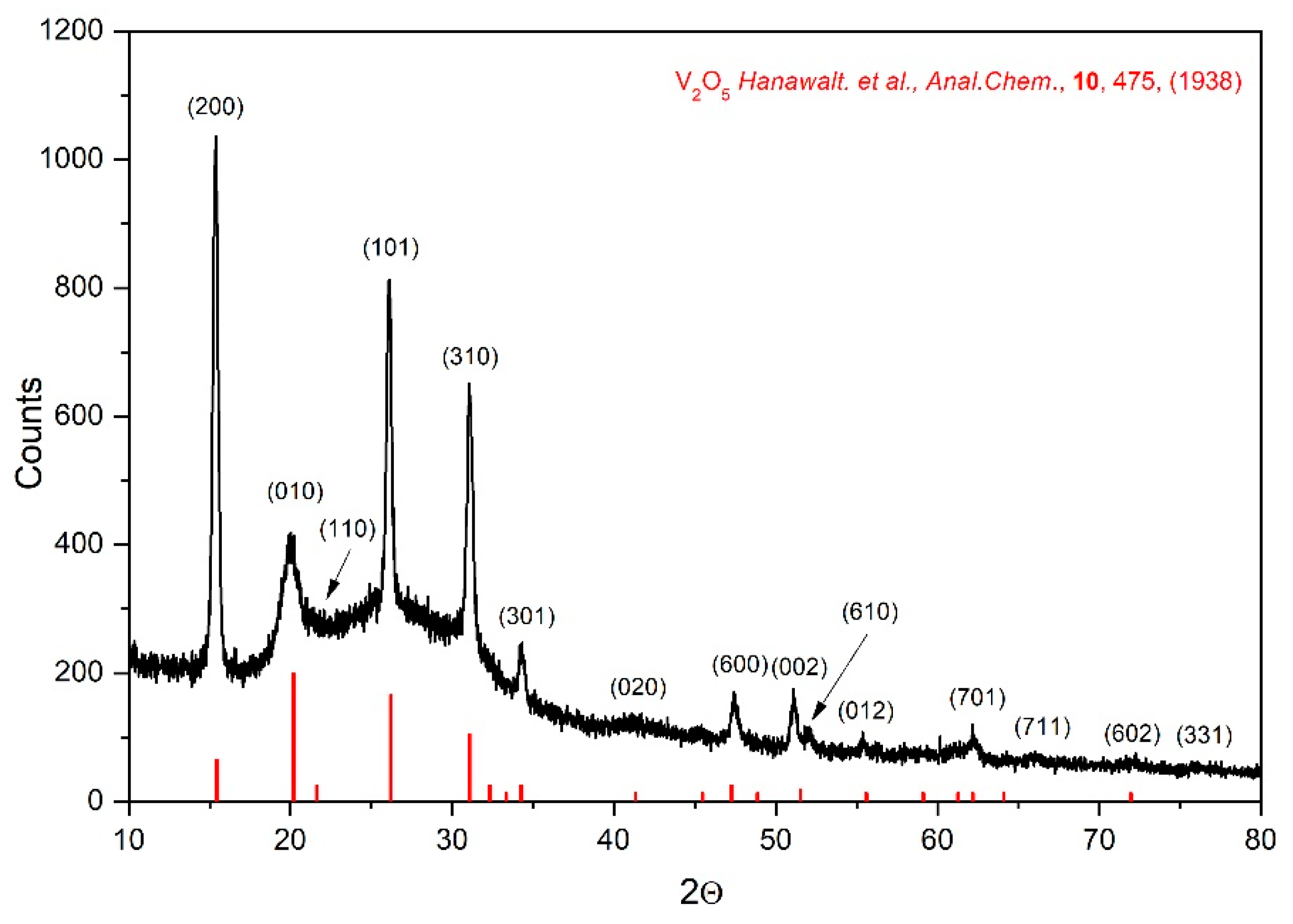
Figure 3 demonstrates X-ray diffraction pattern of as sputtered VO
x thin film. The experimental data were interpreted using XRD patterns distributed by the International Centre for Diffraction DATA –ICDD. As can be seen, the film is weakly crystallized. Using selected peaks: (1 0 1), (4 0 0), (3 0 1) and (2 2 1) the V
2O
5 orthorhombic phase (space group Pmmn) was identified. The determined lattice parameters (
a = 1.15 nm;
b = 0.44 nm;
c = 0.356 nm well agree with that literature reports [
7,
8].
Crystallite sizes,
dXRD were calculated from the X-ray broadening of the selected peaks according to Scherrer’s method:
where λ = 0.154056 nm is X-ray wavelength (CuK
α), 𝛥(2θ) denotes the broadening of the XRD peak at half of its maximum intensity, and θ represents the Bragg diffraction angle.
Parameter dXRD was determined for 6 most intense peaks. Determined values of dXRD = (26 ± 5) nm.
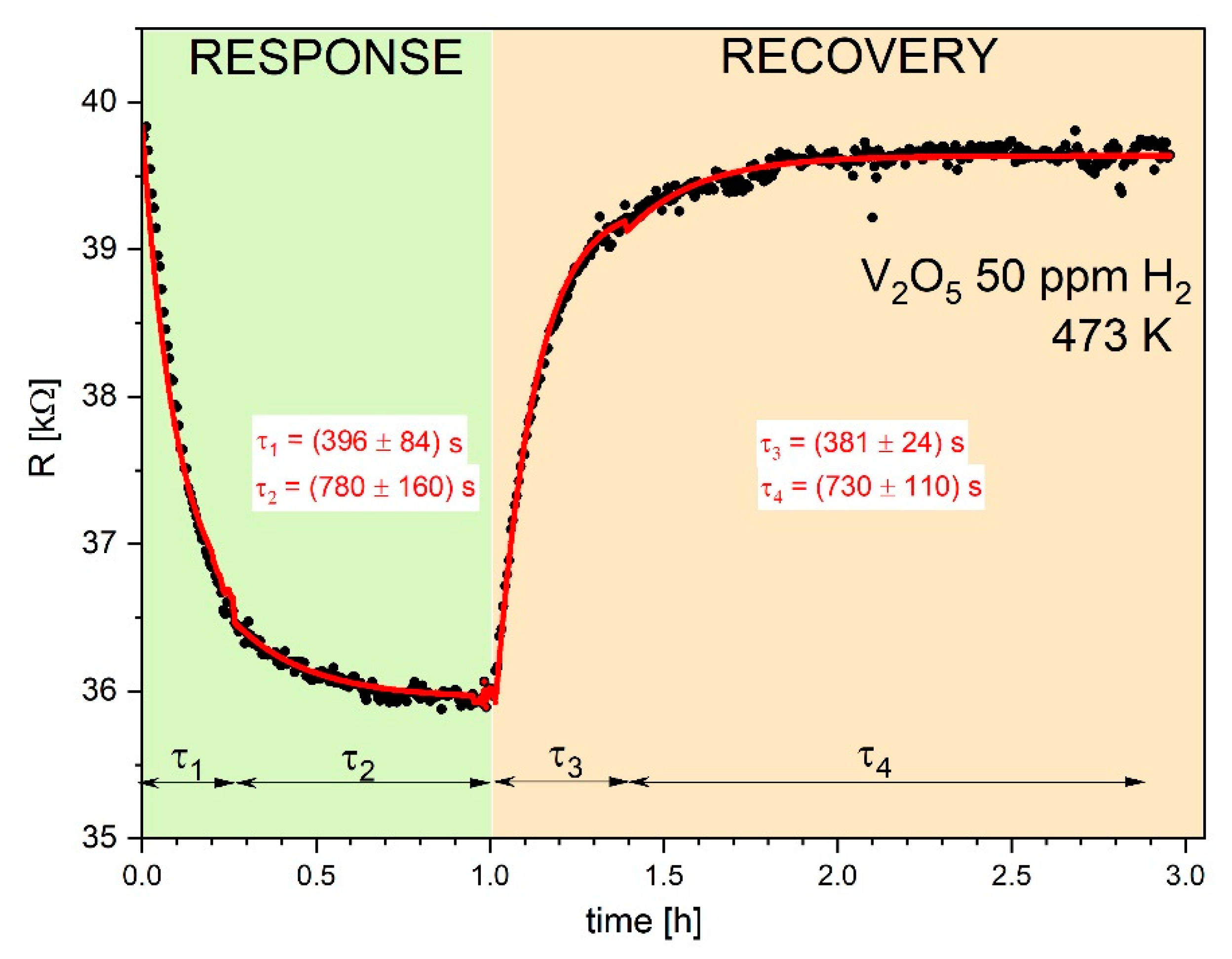
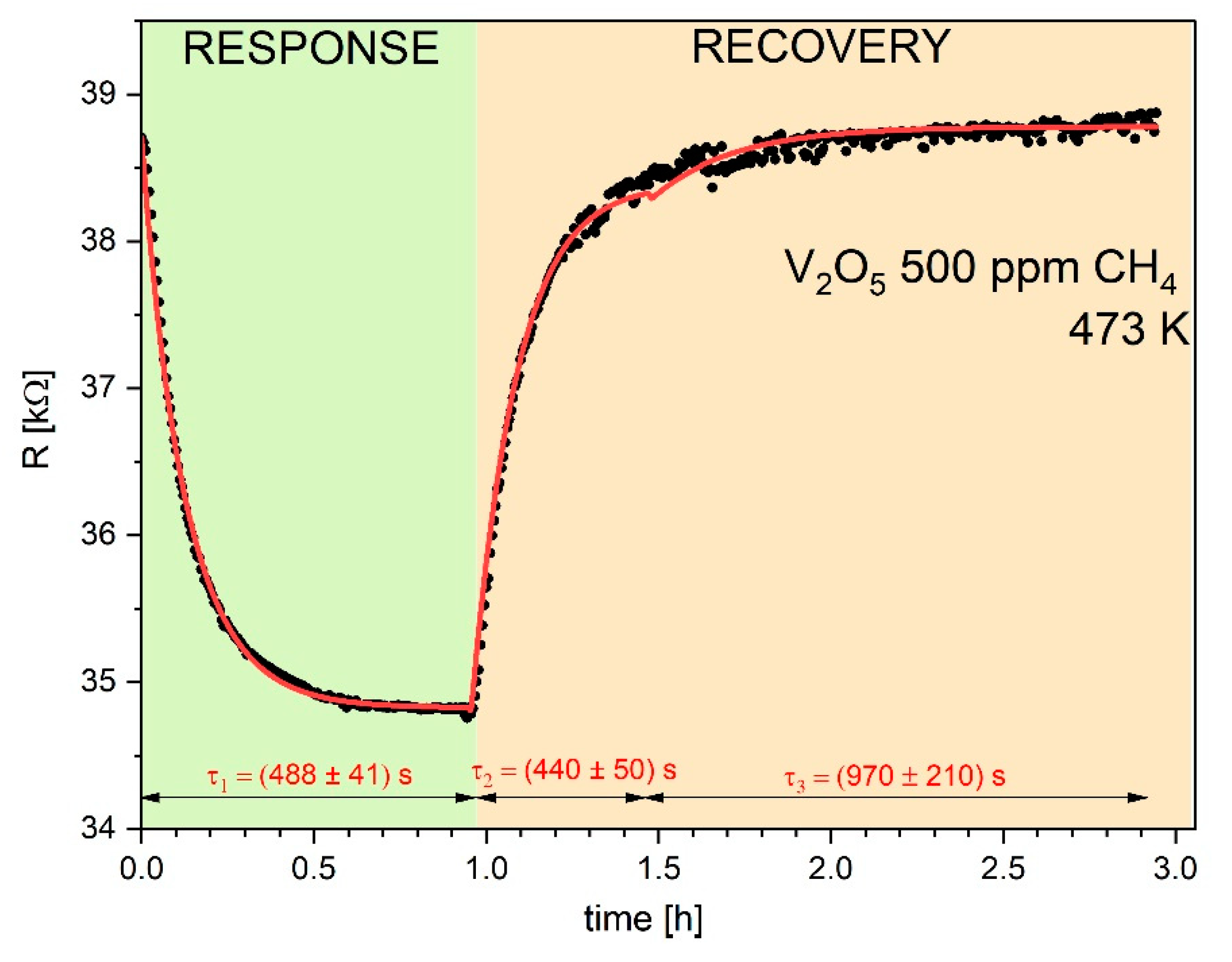
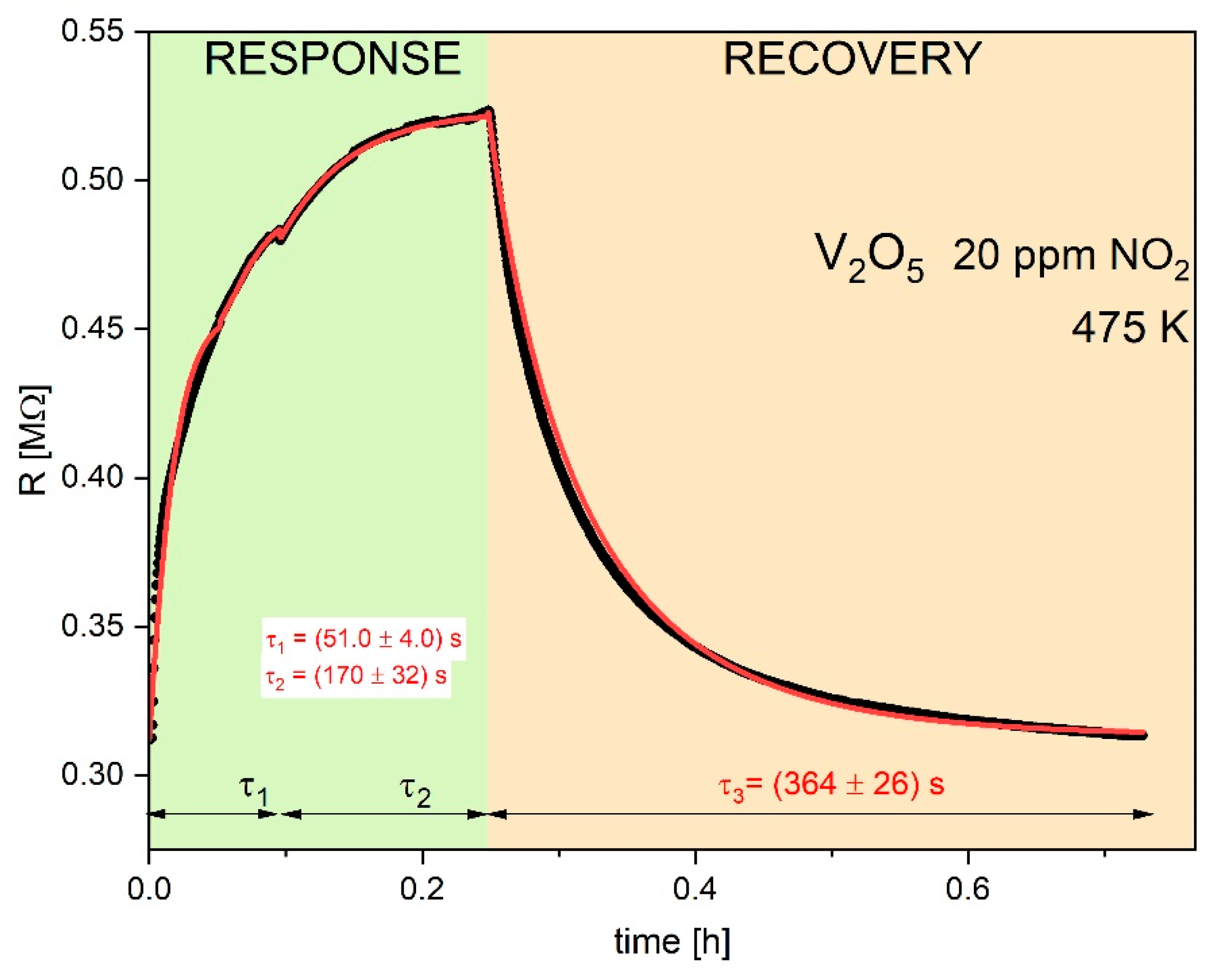
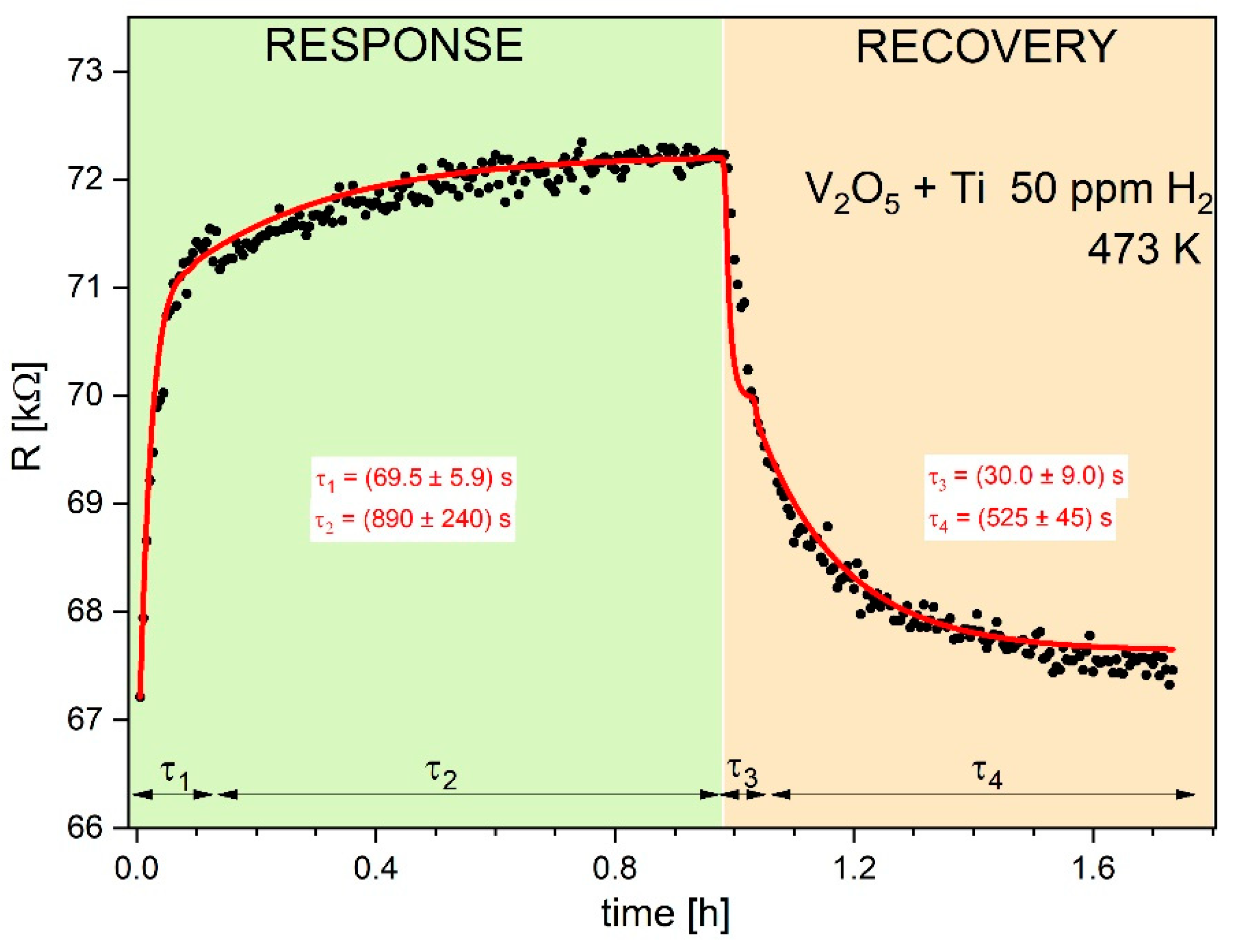
Figure 4,
Figure 5 and
Figure 6 display typical resistance characteristics (sensor responses and recoveries) to 50 ppm of hydrogen, to 500 ppm of methane and 20 ppm NO
2 , respectively for V
2O
5 thin films at 473 K. Points on these figures illustrate experimental results of
R vs. time, whereas the lines represent theoretical plots of the Equation (12).
Attempts to fit the experimental data using a simple single Langmuir isotherms from Equation (12) was poor with the squared
R2 of the fitting coefficient were poor (
R2 << 0.9). The satisfactory fitting results (with
R2 > 0.95) were achieved using twice Equation (12) with two different parameters of τ. Similar case was observed by Aygiin and Cann [
1] in analysis of the hydrogen sensor responses on CuO/ZnO heterocontacts.
The determined parameters
R2 and τ from the fitting procedure are collected in
Table 2. It is observed quite good agreement between experimental and theoretical dependences.
As can see, there is a systematic decrease in the electrical resistance
R upon exposure to reducing gases used as hydrogen and methane. On the other hand, oxidizing gas, used as NO
2 leads to increase in the electrical resistance. Such behavior is typical for the n-type semiconductors and it results from the following defect reaction in V
2O
5-x [
9] (Krőger-Vink defect notation was used):
4.2. Ti-Doped V2O5 Thin Films
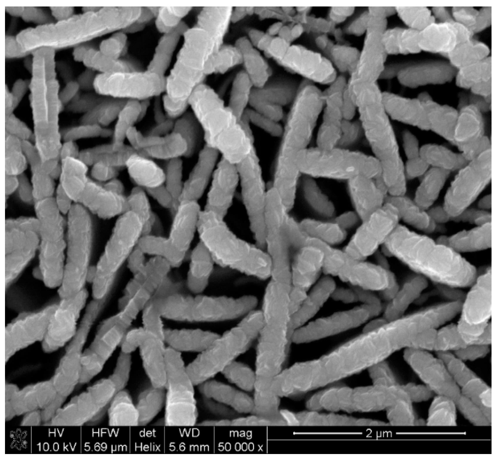
Figure 7 shows the SEM micrograph of Ti-doped vanadium pentoxide thin film. As can be seen, the thin film is composed from prolongated cylindric grains with ca. (1.34 ± 0.44) μm in length and (0.285 ± 0.033) μm diameter.
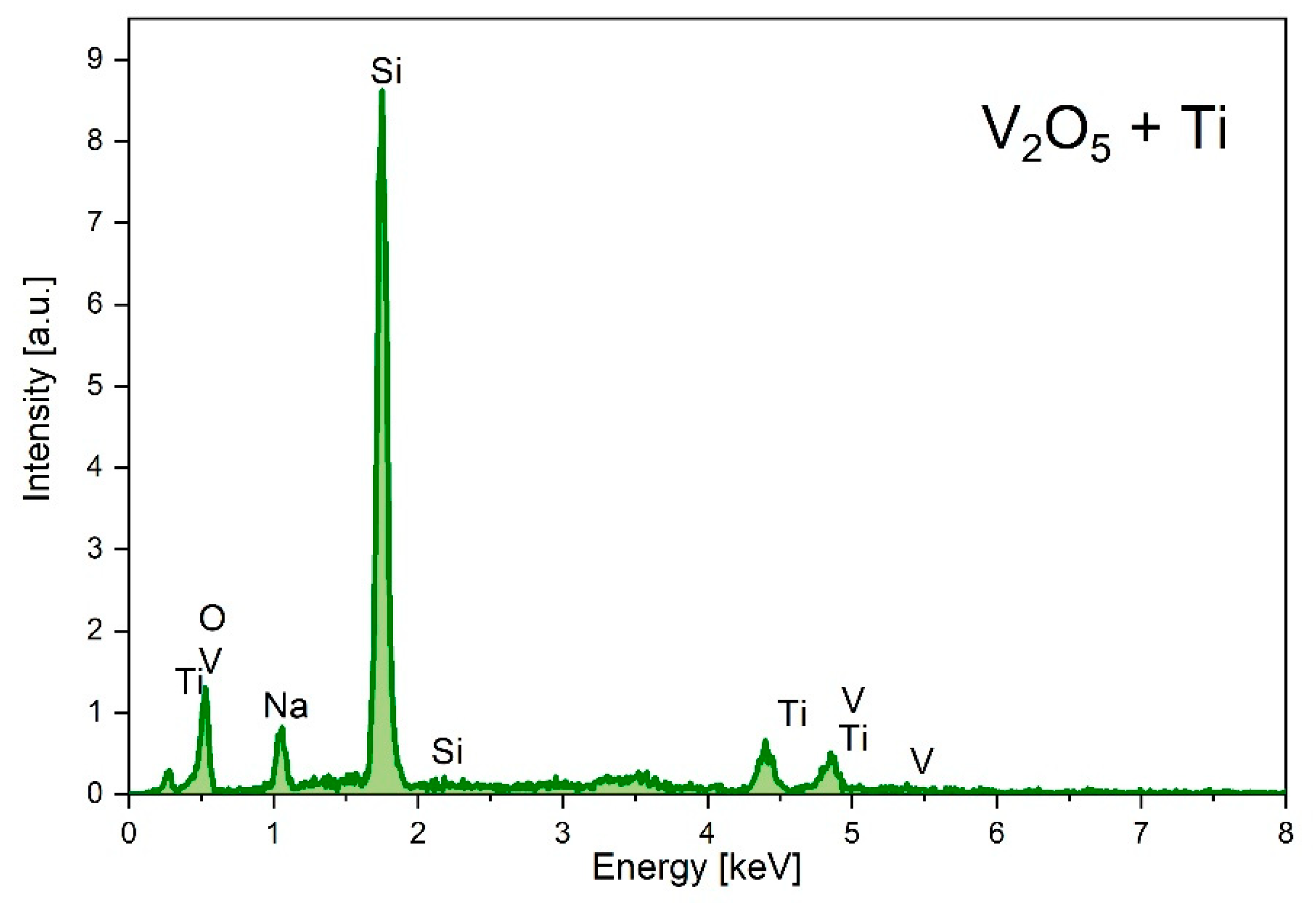
Figure 8 illustrates chemical analysis of the Ti-doped sample made by EDX technique. The high Si peak comes from the silicon support, were as the peaks V and O come from the sensor material. The estimated concentration of the Ti in the sample was about 13.8 at %.
Figure 9 displays resistance characteristic (sensor response and recovery) to 500 ppm of methane for Ti- doped V
2O
5 thin films at 473 K. Analogously as in case of the undoped V
2O
5 sample, the points on the figure illustrate experimental results of
R vs. time, whereas the lines represent theoretical plots of the Equation (12). The determined parameters τ from the estimation experimental values are collected in Table 3. It is observed quite good agreement between experimental and theoretical dependences.
The observed systematic increase in the electrical resistance
R upon exposure to methane (i.e. reducing gas) is typical for the p-type semiconductors and it results from the mechanism of the incorporation TiO
2 into vanadium pentoxide crystal lattice:
Sensor response S was defined for reducing gases as :
And for oxidizing gases as:
Where
R1 represented the electrical resistance upon interaction with target gas and
R0 was the electrical resistance in air. Values of sensor responses
S are collected in
Table 2. The highest
S is observed in case of NO
2 sensor.
Conclusions
Thin films of undoped and Ti-doped vanadium pentoxide exhibit n- and p- type semiconducting property, respectively
The materials show property against both reducing and oxidant gases.
The observed kinetics of the electrical resistivity agree well with the Langmuir’s chemisorption isotherms
Acknowledgments
‘Research project supported by program “Excellence initiative – research university” for the AGH University of Science and Technology.
Conflicts of Interest
The author declare no conflict of interest.
References
- S.Aygiin, D.Cann, Response kinetics of doped CuO/ZnO heterocontacts. J.Phys. Chem. B 2005, 109, 7878–7882. [CrossRef] [PubMed]
- K.Mulkherjee, S.B.Majumder, Analysis of response and recovery kinetics of zinc ferrite as hydrogen gas sensor. J. Appl.Phys. 2009, 106, 064912. [CrossRef]
- G.Mineo, K.Moulaee, G.Neri, S.Mirabella, E.Bruno, H2 detection mechanism in chemoresistive sensor based on low-cost synthesized WO3 nanorods. Sens. Actuators B Chem., 2021, 348, 130704. [CrossRef]
- M.Urso, S.Gianluca Leonardi, G.Neri, S. Patralia,S. Canoci, F.Priolo, S. Mirabella, Room temperature detection and modelling of sub-ppm NO2 by low-cost nanoporous NiO film. Sens. Actuators B Chem., 2020, 305, 127481. [CrossRef]
- M.Censabella, V.Iacono, A.Scandurra, K.Moulaee, G.Neri, F.Ruffino, S.Mirabella, Low temperature detection of nitric oxide by CuO nanoparticles synthesized by pulsed laser ablation. Sens. Actuators B Chem., 2022, 358, 131489. [CrossRef]
- D.Wlodek, K.Cablow, F.Consadori, Kinetic model of thermally cycled tin oxide gas sensor. Sens. Actuators B 1991, 3, 123–127. [CrossRef]
- R.W.G.Wyckoff, Crystal Structures, 2nd ed. 1964 (Interscience .New York) v.2.
- Chakarbarti, K.Hermann, R.Druzinic, M.Witko, F.Wagner, M.Petersen, Geometric and electronic structure of vanadium pentoxide: A density functional bulk and surface study. Phys.Rev. B 1999, 59, 10583–10590. [CrossRef]
- K.Schneider, Defect structure and electrical properties of vanadium pentoxide thin films. J. Mater. Sci: Mater. Electron. 2022, 33, 10410–10422. [CrossRef]
|
Disclaimer/Publisher’s Note: The statements, opinions and data contained in all publications are solely those of the individual author(s) and contributor(s) and not of MDPI and/or the editor(s). MDPI and/or the editor(s) disclaim responsibility for any injury to people or property resulting from any ideas, methods, instructions or products referred to in the content. |
© 2024 by the author. Licensee MDPI, Basel, Switzerland. This article is an open access article distributed under the terms and conditions of the Creative Commons Attribution (CC BY) license (https://creativecommons.org/licenses/by/4.0/).


