1. Introduction
Recently, much attention has been directed to metal oxide thin films due to their remarkable and captivating optical, optoelectronic, and electrical characteristics. These metal oxides exhibit exceptional thermal stability and possess a significant absorption coefficient. The distinctive characteristics of these metal oxides render them well-suited for various applications, such as optical memory devices, window layers for solar cells, IR sensors, and photodetectors. Photodetection converts light into an electrical signal, which is crucial in many modern technologies [
1].
Among the widely used materials for photodetection are semiconductors such as silicon [
2], III-V compounds like gallium arsenide [
3], and other materials based on nanomaterials, including graphene [
4,
5,
6,
7,
8], 2D transition metal dichalcogenides (TMDCs) [
9], and graphitic-carbon nitride (g-C3N4) [
10,
11]. Graphene was the initial 2D material explored for photodetectors, capitalizing on its remarkable electrical characteristics, notably its impressive carrier mobility [
6,
7] and a high-speed bandwidth of up to 40 GHz [
5,
6,
7]. However, the absence of a bandgap in graphene results in dark currents, contributing significantly to signal noise. This limitation substantially restricts its broader applications in photodetection. Among TMDs, molybdenum disulfide (MoS
2) has attracted much interest in the last decade due to its high mobility, high optical absorption capacity and tunable bandgap [
12,
13,
14]. These materials have specific properties that make them suitable for various wavelength ranges and diverse applications, ranging from detecting low light levels to high-speed optical communication. Exploring the properties of these materials opens up exciting possibilities for enhancing photodetection performance and expanding its applications in areas such as remote sensing, medicine, and quantum technology.
The use of advanced materials in developing optoelectronic devices, such as photodetectors, has become crucial to meet increasing performance requirements. A new material, NiV
2O
6, a compound of nickel and vanadium, emerges as a promising candidate for photodetection applications due to its inimitable properties. NiV
2O
6 has intrinsic characteristics that make it an attractive material, including its tunable optoelectronic properties. The ease of large-scale manufacturing of NiV
2O
6, its wide band gap of 2.4 eV [
15,
16], sensitive optical responses, high absorption coefficient exceeding 10
6 m
-1, and its porous structure make it an attractive material for various applications.
For instance, light trapping technique approach has widely used as an appropriate way to improve the efficiency of the solar cell using generally the Silicon bottom texturing or a transparent conductor in the superstrate-type cells, compared to non-porous structures [
17]. Further, the high efficiency photoelectrochemical water splitting was reported for porous TiO
2, almost two times than that of the photoanode formed by TiO
2 nanoparticle-based films (P25) [
18].
In the present work, we emphasize the fundamental properties of porous NiV2O6 film, its synthesis process, and its potential as a light-sensitive material for photodetectors, providing insight into its possibilities in optical sensing.
2. Materials and Methods
This work used a spray pyrolysis process to fabricate NiV2O6 layers. The precursor solution is produced from the chemical reaction between two solutions. We added 40 ml of 0.1 M nickel nitrate Ni (NO3)2 to 60 ml of 0.2 M of ammonium vanadate NH4VO3. The mixture was stirred for 15 minutes. The heated glass slides were sprayed with the NiV2O6 solution for 4, 6, and 9 minutes. The spray pyrolysis settings were adjusted at the substrate temperature of 250 °C, 5 ml/min for the flow rate, and 3 atm for the air pressure. The distance between the nozzle and the substrate has been adjusted to 30 cm. Using the Bruker-Dektak stylus profiler, the thickness of the NiV2O6 layers has been measured (S1 is 0.86 µm, S2 is 2.41 µm, and S3 is 2.94 µm). The structural analysis of the phase formation was detected by X-ray diffraction (XRD) type a four-circle Bruker Discover D8 diffractometer with CuKα = 1.5406 Å (D8 Advance, Bruker, Germany). The vibrational analyses were recorded with a micro-Raman Renishaw spectrometer using a green laser excitation source (532 nm). The microstructure and the composition of the NiV2O6 films were investigated by a scanning electron microscope (SEM) Quanta 200 FEG equipped with energy-dispersive X-ray spectroscopy (EDX). The optical properties were analyzed using a JASCO V- 670 UV-vis-near IR spectrometer. The thickness and roughness of the films were determined by the Bruker profilometer (model: Dektak XT). The photo-response of the deposited samples is characterized under a 1.5 G AM spectrum of an Ossila solar simulator (model No. G2009A1) at a constant applied bias of 3V using Palmsens 4 electrical measurements station by two probe method at room temperature.
3. Results and Discussion
3.1. Microstructural and Surface Morphology Study
The microstructural characteristics of the prepared NiV
2O
6 films were examined by scanning electron microscope, as shown in
Figure 1. SEM images reveal complex and heterogeneous three-dimensional surfaces featuring irregularly dispersed pores of varying sizes and shapes. Image (a) of sample S1 exhibits the texture of a dense and porous structure with predominantly superficial pores. In contrast, images (b and c) of samples S1 and S2 depict deeper pores, resulting in significantly larger specific surface areas.
The porous and meshing structure of NiV
2O
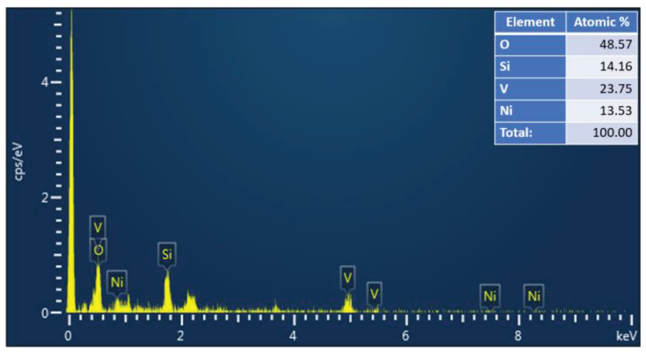
6 makes it an attractive material for various applications such as photodetection and gas sensors, which will benefit from a large specific surface area. Moreover, the EDX spectra of the elaborated samples are illustrated in
Figure 2. The EDX spectra displayed the existence of Ni, V, and O peaks in all samples, and their atomic ratios are 1:2: 6, respectively.
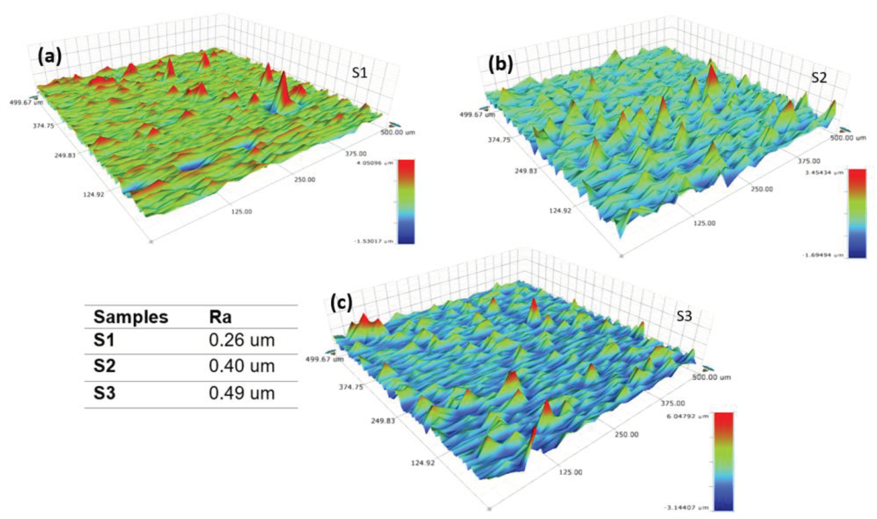
On the other hand, the roughness and surface morphology of the NiV
2O
6 films were assessed through mapping using a profilometer.
Figure 3a–c present 3D micrographs of NiV
2O
6 thin films captured in a scanning area of (0.5 × 0.5) mm2. These images clearly illustrate the correlation between surface roughness and film thickness. It is noted that the surface roughness escalates as the film thickness increases. Specifically, the average film roughness increases from 0.26 µm to 0.49 µm as the film thickness increases. This trend will increase the quantity of trapped light and, therefore, the light-material reaction, i.e., the absorption for the very thick samples S2 and S3.
3.2. Structural Investigation
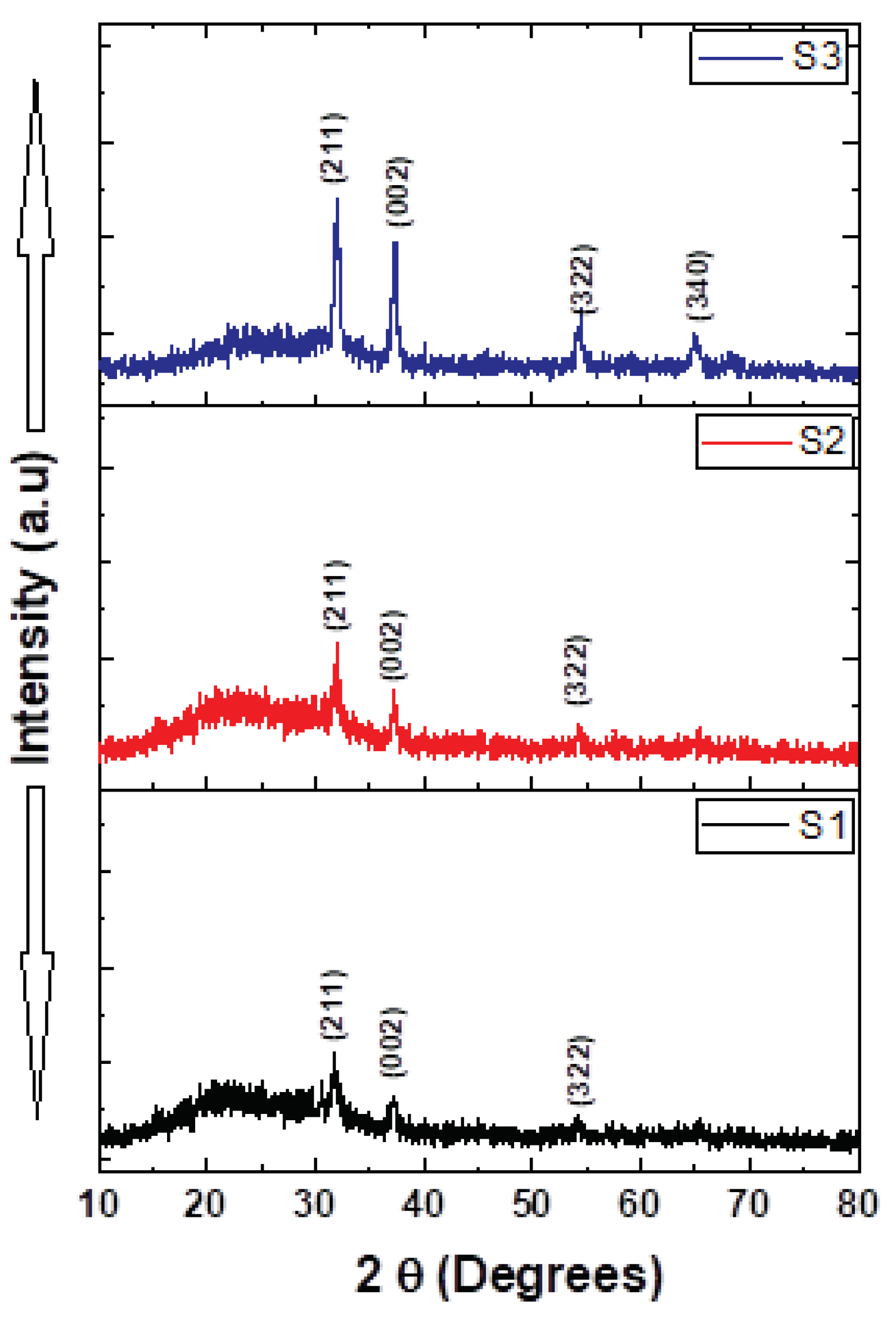
Figure 4 depicts the XRD of the NiV
2O
6 thin films, in the limit of detection device. The figure displays only four distinguished diffraction patterns. According to the Standard JCPDS file no. 76-0359, the observed peaks might be indexed with (211), (002), (322), and (340) planes of the NiV
2O
6 single triclinic structure. Complementary structural information is needed to confirm this assumption
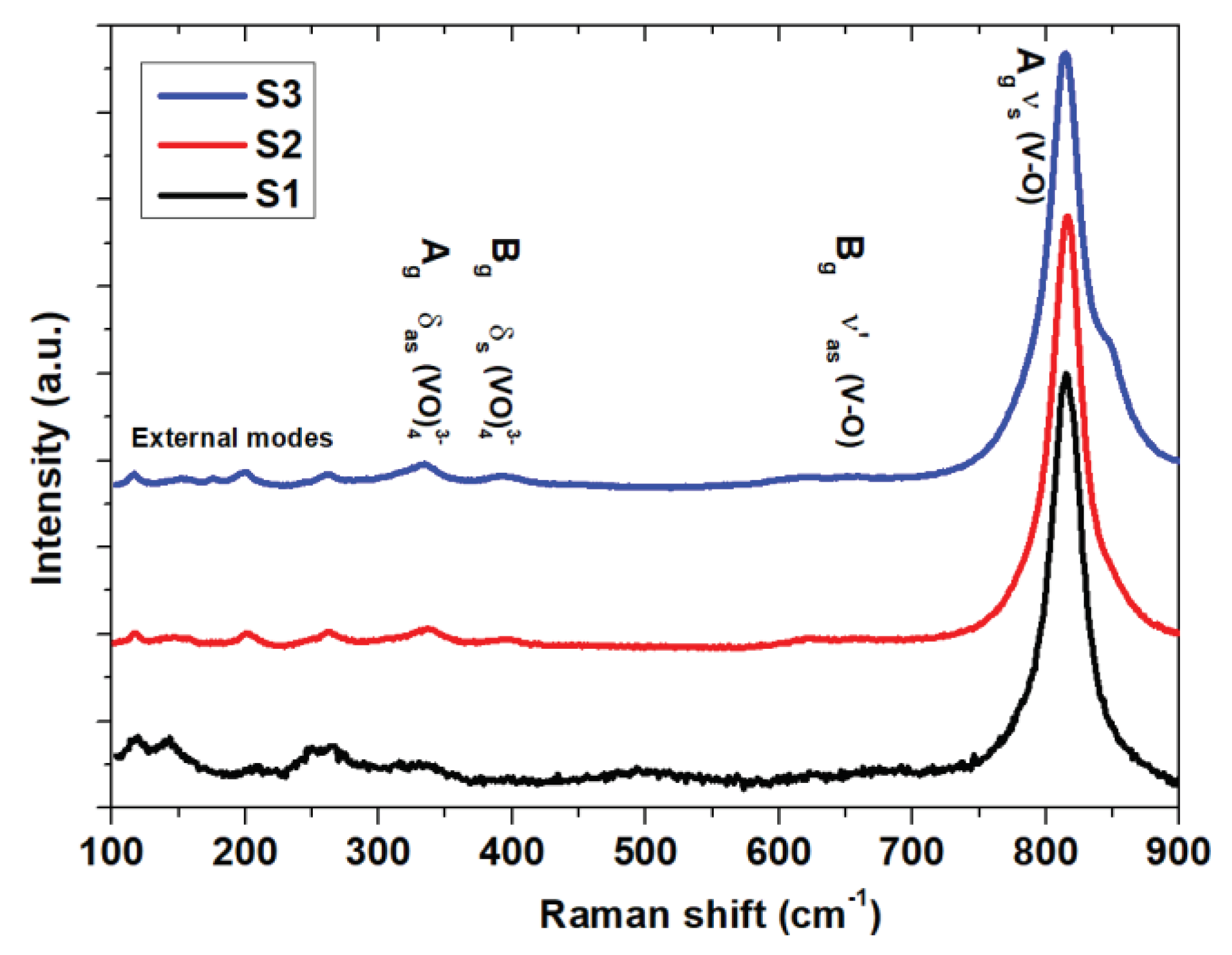
Raman spectroscopy is an effective tool for investigating structural and bonding characteristics, providing valuable insights into materials’ local structure, crystallization and electronic properties. The Raman bands of NiV
2O
6 in the 100-900 cm
−1 range were obtained with varying spray times, as depicted in
Figure 5.
Consistent Raman bands at 327, 367, 647, and 816 cm
–1 were observed across all samples, indicative of the distinctive vibrational bands of the triclinic NiV
2O
6 system. A comparison of vibration modes for different materials like NiV
2O
6 is summarized in
Table 1. The prominent band at 816 cm
−1 corresponds to the shorter symmetric V–O stretching mode (Ag), while the weaker band at 647 cm
−1 is associated to the short (Bg) asymmetric V–O stretching modes [
19]. Additionally, the asymmetric and symmetric bending vibrations of the VO
4 tetrahedron were identified at 327 and 367 cm
−1, respectively [
20]. Alternatively, within our sample S3, we detected a shoulder at 846 cm
−1, which can be ascribed to a division arising from the lower symmetry of the monoclinic structure [
21]. The vibrations of the crystal lattice (external modes) are responsible for the peaks observed at 138 and 205 cm
−1 [
22].
3.3. Optical Study
The absorption coefficient (
) was determined using the formula [
25]:
where d represents the film thickness, T signifies transmittance, and R is the reflectance of the samples. The optical bandgap energy (Eg) was derived from the absorption coefficient (
) through the application of the Tauc model. [
26,
27]:
where
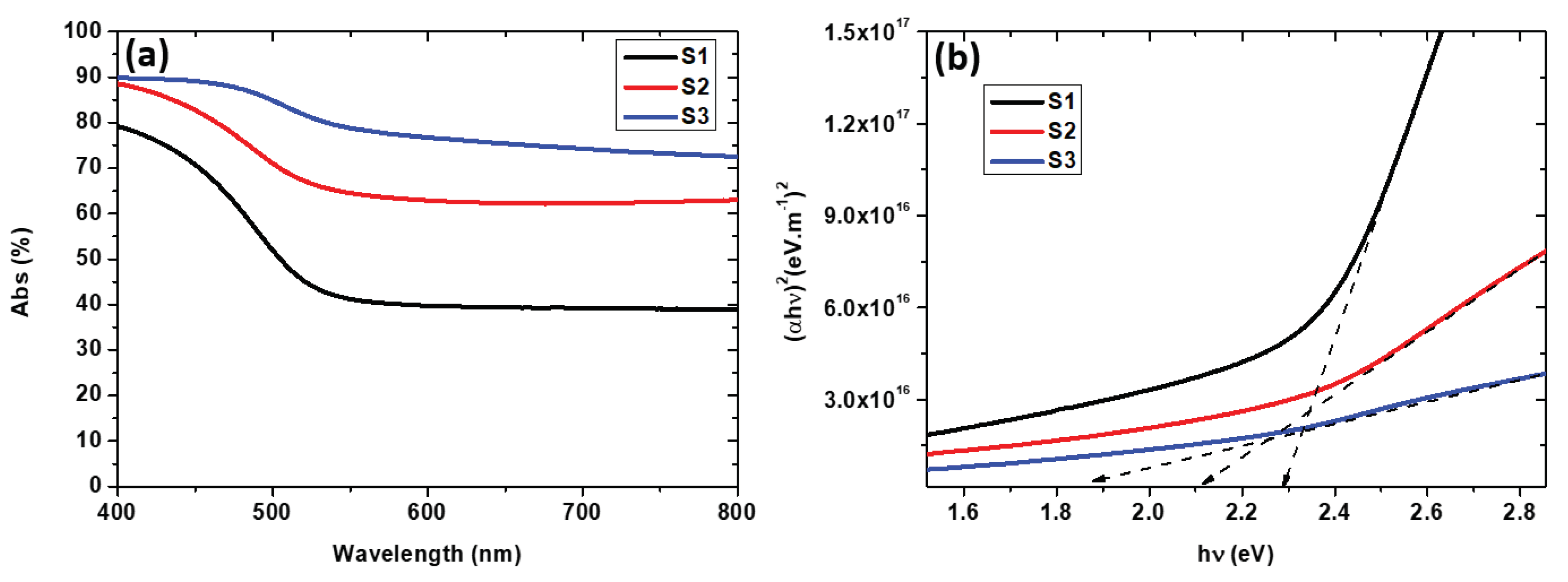
represents the photon energy, A is a constant, Eg is the optical band gap, and n is an exponent indicating the nature of optical absorption. For a direct authorized transition, m = 1/2; for an indirect authorized transition, m = 2; for a direct forbidden transition, m = 3/2; and for an indirect forbidden transition, m = 3. The bandgap energy (Eg) of the developed NiV
2O
6 is obtained by plotting (αhν)
2 versus photon energy (
Figure 6b)
The dielectric function
is a critical factor for the optical properties of a semiconductor, which could be defined by the below (3) [
28,
29]:
where
is the real part of the dielectric function, and
is the imaginary parts of the dielectric functions, which can represent electronic transitions linked to conduction and valence bands.
The refractive index is a characteristic of a medium, describing the behavior of light in it, whose complex form
[
28], where n represents the refractive index, and k refers to the extinction coefficient calculated by the following equation k=
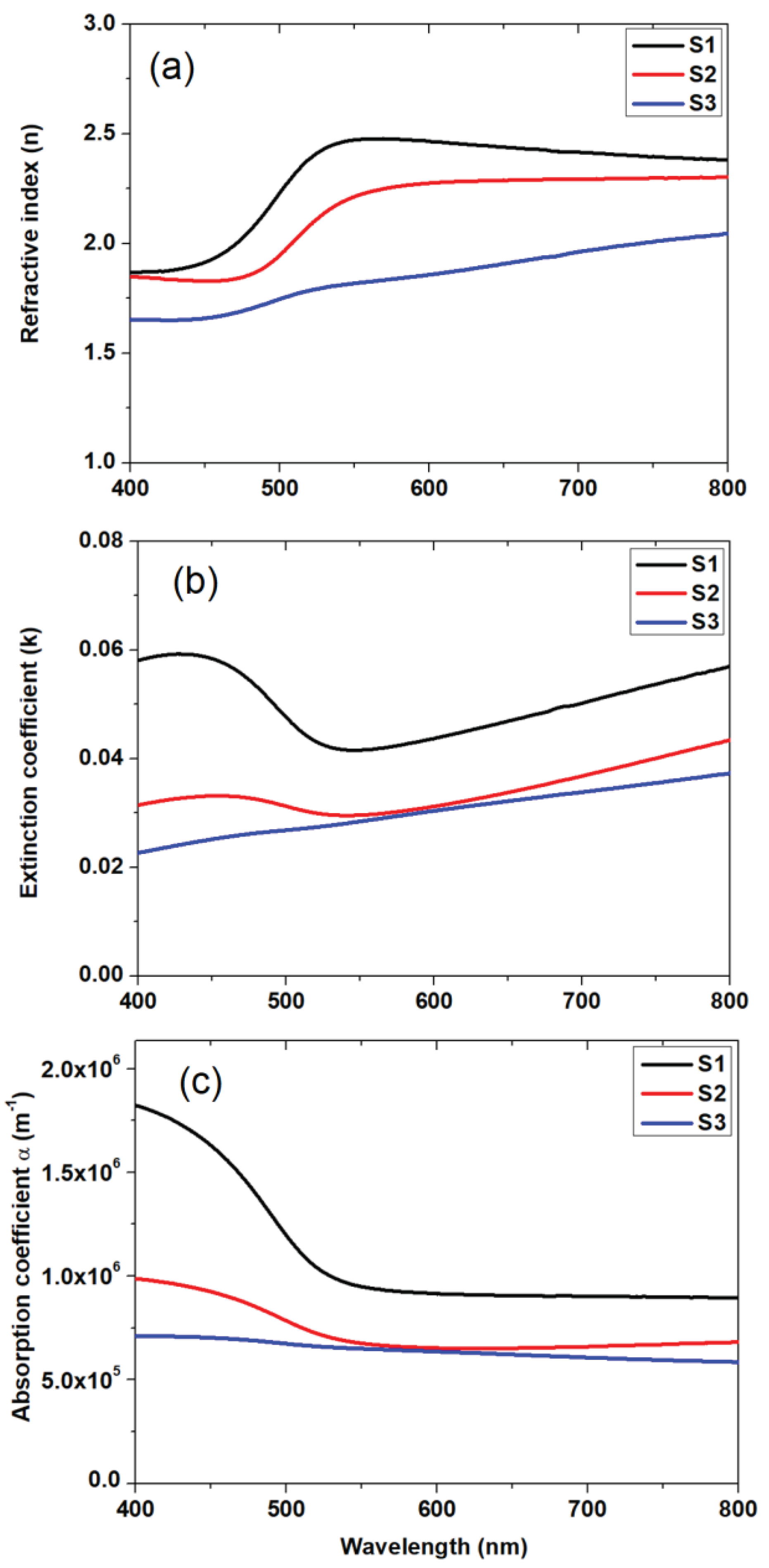
. The variations of the absorption coefficient
, the extinction coefficient k and the refractive index n as a function of wavelength are given in
Figure 7a–c. These parameters inform us about the loss of energy in the medium, i.e., the absorption of the photons. NiV
2O
6 is a promising material for fabricating photodetector devices due to its wide optical bandgap energy of 2.3 eV, and its high optical absorption coefficient > 10
6 m
-1 [
30]. It is important to emphasize that the porous structure of our samples leads to optical data relative to this effective medium (NiV
2O
6 + the pores). These datado notuniquely refer to the NiV
2O
6 phase of the spongy material. It is well known that NiV
2O
6 is a semi-conductor and one therefore expects a very low absorption for energies below the bandgap, in contrast to what can be observed in our samples where the absorbed energy is higher than 40% for the longer wavelengths. This is owed to the highly porous structure of the material. As the sample S1 exhibits a higher density and a less spongy structure than the other two samples its band gap is near to that one expected for the NiV
2SO
6, while for S2 and S3 the lower bandgaps just reflect their more porous microstructure. This is underlined by the very high energy fraction absorbed even at higher wavelengths for these samples. Therefore, this relative decrease of Eg does not mean that the electronic structure of the NiV
2SO
6 phase has changed (there is no quantum confinement for instance) for S2 and in S3.
3.4. Photodetector Application
In this work, the sensitivity was studied with different film thicknesses at constant light source intensity (100 mW/cm
2) and effective illumination area (0.1 cm
2) (
Figure 8). The sensitivity depends on the intensity of the light source and the effective illumination area. The photodetector’s performance is evaluated by a key parameter known as sensitivity (S), which can be defined as [
30]:
where Iph is the photocurrent, and it is equal I
light - I
dark, moreover, I
dark is the dark current, and I
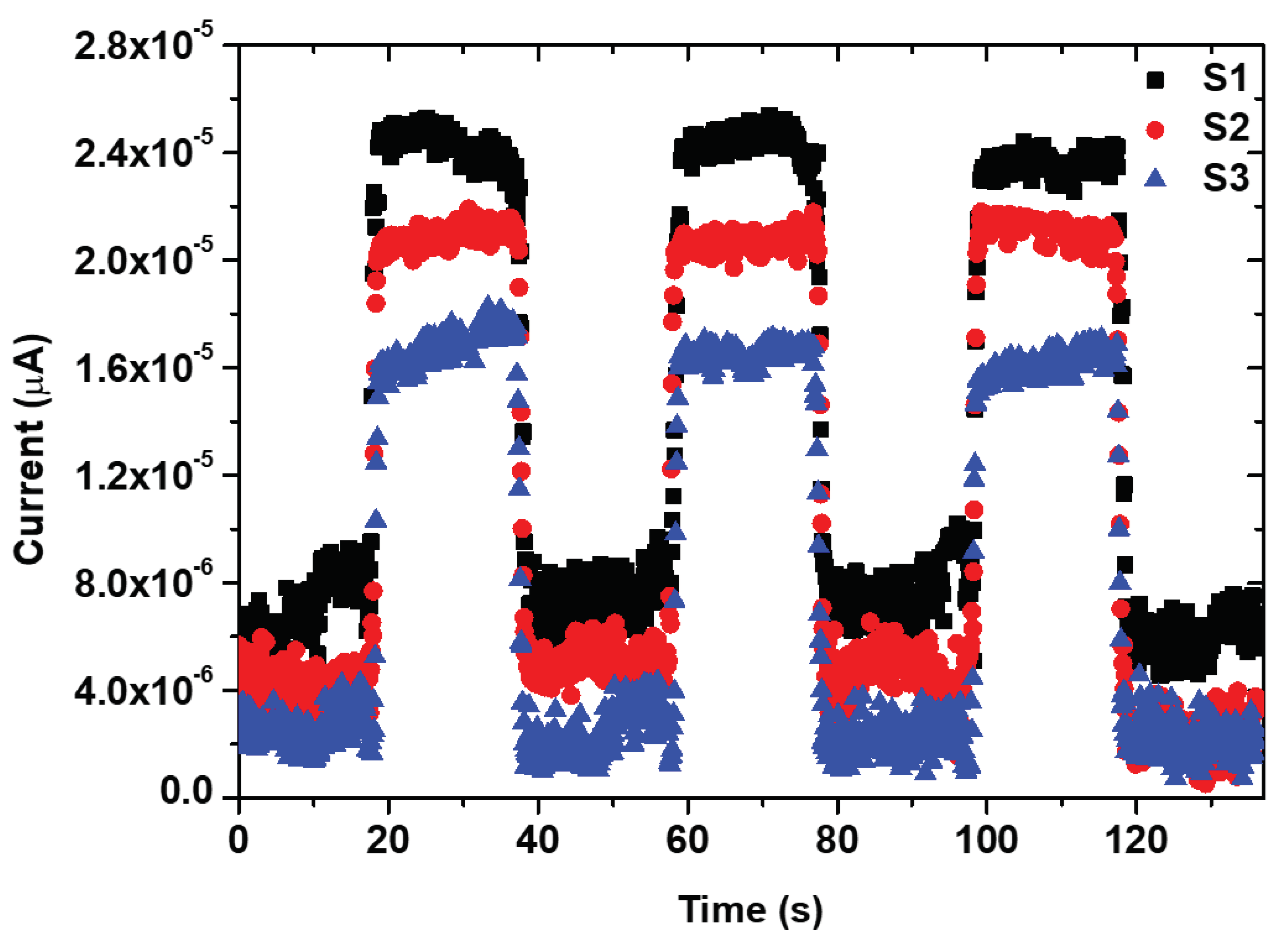
light is the light current. At a bias voltage of 3V, the sensitivity values for samples S1, S2, and S3 were computed and found to be around 328, 511, and 433, respectively, as presented in
Table 2. It is observed that the sensitivity of the layers increases with the boost in layer thickness due to the increase in the optical absorption of the films.
Rise and decay times are crucial parameters in assessing photodetector performance. For a single on/off cycle, the rise times were determined to be approximately 0.62, 0.29, and 0.43 seconds. In contrast, decay times were found to be 1.19, 0.52, and 0.69 seconds at a bias voltage of 3 V for samples S1, S2, and S3, respectively (
Figure 9). Sample S2 exhibited very fast rise and decay times, as revealed by the photo-response time results
4. Conclusions
This research involved the successful fabrication of NiV2O6 thin films on glass substrates through the application of the spray pyrolysis technique. The influence of spray time on the optical properties of NiV2O6 films has been investigated. A triclinic structure was obtained for all samples. The reflectance and transmission spectra are utilized to compute the optical constants, including the refractive index (n) and extinction coefficient (k). With increased film thickness, the effective band gap value decreases from 2.3 eV to 1.9 eV. The film’s photo response parameters, like sensitivity (S), increase with film thickness. The fastest rise and fall times of 0.29 s and 0.52 s were obtained for sample S2.
However, it is interesting to point out herein that the properties obtained are not intrinsic to the films alone. The specific microstructure in which the pores take place, and change depth with increasing thickness, plays a key role in trapping light and changing the behavior that would be observed if the microstructure of the films were continuous and smooth. The versatile method used herein for processing films with high active area is promising for a wide range of applications.
Author Contributions
Conceptualization, A.L. and I.M.E; validation, A.L., A.Z.; formal analysis, A.K.; investigation, A.K., I.H.A and A.C.; data curation, A.K. and I.M.E; visualization, I.H.A and A.C.; writing—original draft preparation, A.K.; writing—review and editing, A.L, A.Z and I.M.E, supervision, A.Z.; All authors have read and agreed to the published version of the manuscript.
Funding
This work was supported by PARS (ANR-DFG) project N°22003
Data Availability Statement
Not applicable.
Conflicts of Interest
The authors declare no conflict of interest.
References
- Banerjee, D.; Chattopadhyay, K.K. Chapter 5 - Hybrid Inorganic Organic Perovskites: A Low-Cost-Efficient Optoelectronic Material; Thomas, S., Thankappan, A.B.T.-P.P., Eds.; Academic Press, 2018; pp. 123–162. ISBN 978-0-12-812915-9. [Google Scholar]
- Piels, M.; Bowers, J.E. 1 - Photodetectors for silicon photonic integrated circuits; Nabet, B.B.T.-P., Ed.; Woodhead Publishing, 2016; pp. 3–20. ISBN 978-1-78242-445-1. [Google Scholar]
- Channel, E.T. Fast Response GaAs Photodetector Based on Constructing Electron Transmission Channel. 2021; 1–8. [Google Scholar]
- Kotbi, A.; Imran, M.; Kaja, K.; Rahaman, A.; Ressami, E.M.; Lejeune, M.; Lakssir, B.; Jouiad, M. Graphene and g-C3N4-Based Gas Sensors. J. Nanotechnol. 2022, 2022, 9671619. [Google Scholar] [CrossRef]
- Chen, X.; Shehzad, K.; Gao, L.; Long, M.; Guo, H.; Qin, S.; Wang, X.; Wang, F.; Shi, Y.; Hu, W.; et al. Graphene Hybrid Structures for Integrated and Flexible Optoelectronics. Adv. Mater. 2020, 32, 1902039. [Google Scholar] [CrossRef]
- Vicarelli, L.; Vitiello, M.S.; Coquillat, D.; Lombardo, A.; Ferrari, A.C.; Knap, W.; Polini, M.; Pellegrini, V.; Tredicucci, A. Graphene field-effect transistors as room-temperature terahertz detectors. Nat. Mater. 2012, 11, 865–871. [Google Scholar] [CrossRef] [PubMed]
- Schuler, S.; Muench, J.E.; Ruocco, A.; Balci, O.; Thourhout, D. van; Sorianello, V.; Romagnoli, M.; Watanabe, K.; Taniguchi, T.; Goykhman, I.; et al. High-responsivity graphene photodetectors integrated on silicon microring resonators. Nat. Commun. 2021, 12, 3733. [Google Scholar] [CrossRef]
- Guo, X.; Wang, W.; Nan, H.; Yu, Y.; Jiang, J.; Zhao, W.; Li, J.; Zafar, Z.; Xiang, N.; Ni, Z.; et al. High-performance graphene photodetector using interfacial gating. Optica 2016, 3, 1066–1070. [Google Scholar] [CrossRef]
- Li, Y.; Li, L.; Li, S.; Sun, J.; Fang, Y.; Deng, T. Highly Sensitive Photodetectors Based on Monolayer MoS2 Field-Effect Transistors. ACS Omega 2022, 7, 13615–13621. [Google Scholar] [CrossRef] [PubMed]
- Kotbi, A.; Benyoussef, M.; Ressami, E.M.; Lejeune, M.; Lakssir, B.; Jouiad, M.; Hills, V. Gas Sensors Based on Exfoliated g-C 3 N 4 for CO 2 Detection. 2022. [Google Scholar]
- Fang, H.; Ma, H.; Zheng, C.; Lennon, S.; Wu, W.; Wu, L.; Wang, H. A high-performance transparent photodetector via building hierarchical g-C3N4 nanosheets/CNTs van der Waals heterojunctions by a facile and scalable approach. Appl. Surf. Sci. 2020, 529, 147122. [Google Scholar] [CrossRef]
- Mouloua, D.; Kotbi, A.; Deokar, G.; Kaja, K.; El Marssi, M.; EL Khakani, M.A.; Jouiad, M. Recent Progress in the Synthesis of MoS2 Thin Films for Sensing, Photovoltaic and Plasmonic Applications: A Review. Materials (Basel). 2021, 14, 3283. [Google Scholar] [CrossRef] [PubMed]
- Nasr, M.; Benhamou, L.; Kotbi, A.; Rajput, N.S.; Campos, A.; Lahmar, A.I.; Hoummada, K.; Kaja, K.; El Marssi, M.; Jouiad, M. Photoelectrochemical Enhancement of Graphene@WS2 Nanosheets for Water Splitting Reaction. Nanomaterials 2022, 12. [Google Scholar] [CrossRef]
- Matras, G.; Marssi, M. El; Kotbi, A. MoS 2 Based Nanomaterial for Light Emitting Diode Applications. Adv. Sci. Eng. Technol. Int. Conf. 2022, 1–5. [Google Scholar] [CrossRef]
- Rahman, M.A.; Akter, M.R.; Khatun, M.R.; Sultana, R.; Sarker, M.A.R. Synthesis and Characterization of High-Quality Polycrystalline Sample NiV 2 O 6 by Solid-State Reaction Technique. 2020, 62, 1024–1032. [Google Scholar] [CrossRef]
- Dang, H.X.; Rettie, A.J.E.; Mullins, C.B. Visible-Light-Active NiV 2 O 6 Films for Photoelectrochemical Water Oxidation. 2015. [Google Scholar]
- Rahim, A. F. A.; Ahmed, M. A.; Razali, N. S. M.; Radzali, R.; Mahmood, A.; Hamzah, I. H.; Noorsal, E. Investigation of Light Trapping from Porous Silicon Surface for the Enhancement of Silicon Solar Cell Performance. Acta Physica Polonica A 2019, 135, 637–642. [Google Scholar] [CrossRef]
- Fang, Y.; Hodgson, R.; Lee, W.C.; Le, H.; Chan, H.W.B.; Hassan, H.M.; Alsohaimi, I.H.; Canciani, G.E.; Qian, R.; Chen, Q. Light trapping by porous TiO2 hollow hemispheres for high efficiency photoelectrochemical water splitting. Phys. Chem. Chem. Phys. 2023, 25, 11253. [Google Scholar] [CrossRef]
- Pereira, R.; Rodrigues, A.D.; Pereira, E.C.; Oliveira, A.J.A. De Sol-gel synthesis of triclinic CoV 2 O 6 polycrystals. Ceram. Int. 2018, 44, 19397–19401. [Google Scholar] [CrossRef]
- Helal, A.; El-sheikh, S.M.; Yu, J. Novel synthesis of BiVO 4 using homogeneous precipitation and its enhanced photocatalytic activity. 2020. [Google Scholar]
- Merupo, V.; Velumani, S.; Ordon, K.; Errien, N.; Szade, J.; Kassiba, A. Structural and optical characterization of ball-milled copper-doped bismuth vanadium oxide (BiVO4). CrystEngComm 2015. [CrossRef]
- Properties, P. Aerosol-Assisted CVD of Bismuth Vanadate Thin Films and Their Aerosol-Assisted CVD of Bismuth Vanadate Thin Films and Their Photoelectrochemical Properties. 2015. [Google Scholar] [CrossRef]
- Bhuvaneswari, M.S.; Selvasekarapandian, S.; Kamishima, O. Vibrational analysis of lithium nickel vanadate. 2005, 139, 279–283. [Google Scholar] [CrossRef]
- Merupo, V.I.; Velumani, S. Structural and Optical properties of Molybdenum doped Bismuth vanadate powders. 2014; 0–4. [Google Scholar] [CrossRef]
- Kotbi, A.; Hartiti, B.; Ridah, A.; Thevenin, P. Characteristics of CuInS2 thin films synthesizes by chemical spray pyrolysis. Opt. Quantum Electron. 2016, 48, 1–9. [Google Scholar] [CrossRef]
- Zhang, S.; Zhang, J.Z.; Han, M.J.; Li, Y.W.; Hu, Z.G.; Chu, J.H. Temperature dependent near infrared ultraviolet range dielectric functions of nanocrystalline (Na0.5Bi0.5)1-xCex(Ti0.99Fe0.01)O3 films. Appl. Phys. Lett. 2014, 104, 0–5. [Google Scholar] [CrossRef]
- Kotbi, A.; Hartiti, B.; Fadili, S.; Ridah, A.; Thevenin, P. Experimental and theoretical studies of CuInS2 thin films for photovoltaic applications. J. Mater. Sci. Mater. Electron. 2019. [CrossRef]
- Zhang, H.; Tang, Y.; Liu, Z.; Zhu, Z.; Tang, X.; Wang, Y. Study on optical properties of alkali metal doped g-C3N4 and their photocatalytic activity for reduction of CO2. Chem. Phys. Lett. 2020, 751, 137467. [Google Scholar] [CrossRef]
- Kotbi, A.; Hartiti, B.; Fadili, S.; Ridah, A.; Thevenin, P. Experimental and theoretical studies of CuInS2 thin films for photovoltaic applications. J. Mater. Sci. Mater. Electron. 2019, 30, 21096–21105. [Google Scholar] [CrossRef]
- Gupta, Y.; Arun, P. Suitability of SnS thin films for photovoltaic application due to the existence of persistent photocurrent. Phys. status solidi 2016, 253, 509–514. [Google Scholar] [CrossRef]
- Veeralingam, S.; Yadav, P.; Badhulika, S. An Fe-doped ZnO/BiVO4 heterostructure-based large area, flexible, high-performance broadband photodetector with an ultrahigh quantum yield. 2020, 9152–9161. [Google Scholar] [CrossRef]
- Mahdi, M.S.; Ibrahim, K.; Hmood, A.; Ahmed, N.M.; Mustafa, F.I.; Azzez, S.A. High performance near infrared photodetector based on cubic crystal structure SnS thin film on a glass substrate. Mater. Lett. 2017, 200, 10–13. [Google Scholar] [CrossRef]
- Wang, Z.; Safdar, M.; Mirza, M.; Xu, K.; Wang, Q.; Huang, Y.; Wang, F.; Zhan, X.; He, J. High-performance flexible photodetectors based on GaTe nanosheets. Nanoscale 2015, 7, 7252–7258. [Google Scholar] [CrossRef] [PubMed]
- Jung, C.; Kim, S.M.; Moon, H.; Han, G.; Kwon, J.; Hong, Y.K.; Omkaram, I.; Yoon, Y.; Kim, S.; Park, J. Highly Crystalline CVD-grown Multilayer MoSe2 Thin Film Transistor for Fast Photodetector. Sci. Rep. 2015, 5, 15313. [Google Scholar] [CrossRef]
|
Disclaimer/Publisher’s Note: The statements, opinions and data contained in all publications are solely those of the individual author(s) and contributor(s) and not of MDPI and/or the editor(s). MDPI and/or the editor(s) disclaim responsibility for any injury to people or property resulting from any ideas, methods, instructions or products referred to in the content. |
© 2024 by the authors. Licensee MDPI, Basel, Switzerland. This article is an open access article distributed under the terms and conditions of the Creative Commons Attribution (CC BY) license (http://creativecommons.org/licenses/by/4.0/).

