3.1. Source Measure Unit (SMU) Functionality Testing
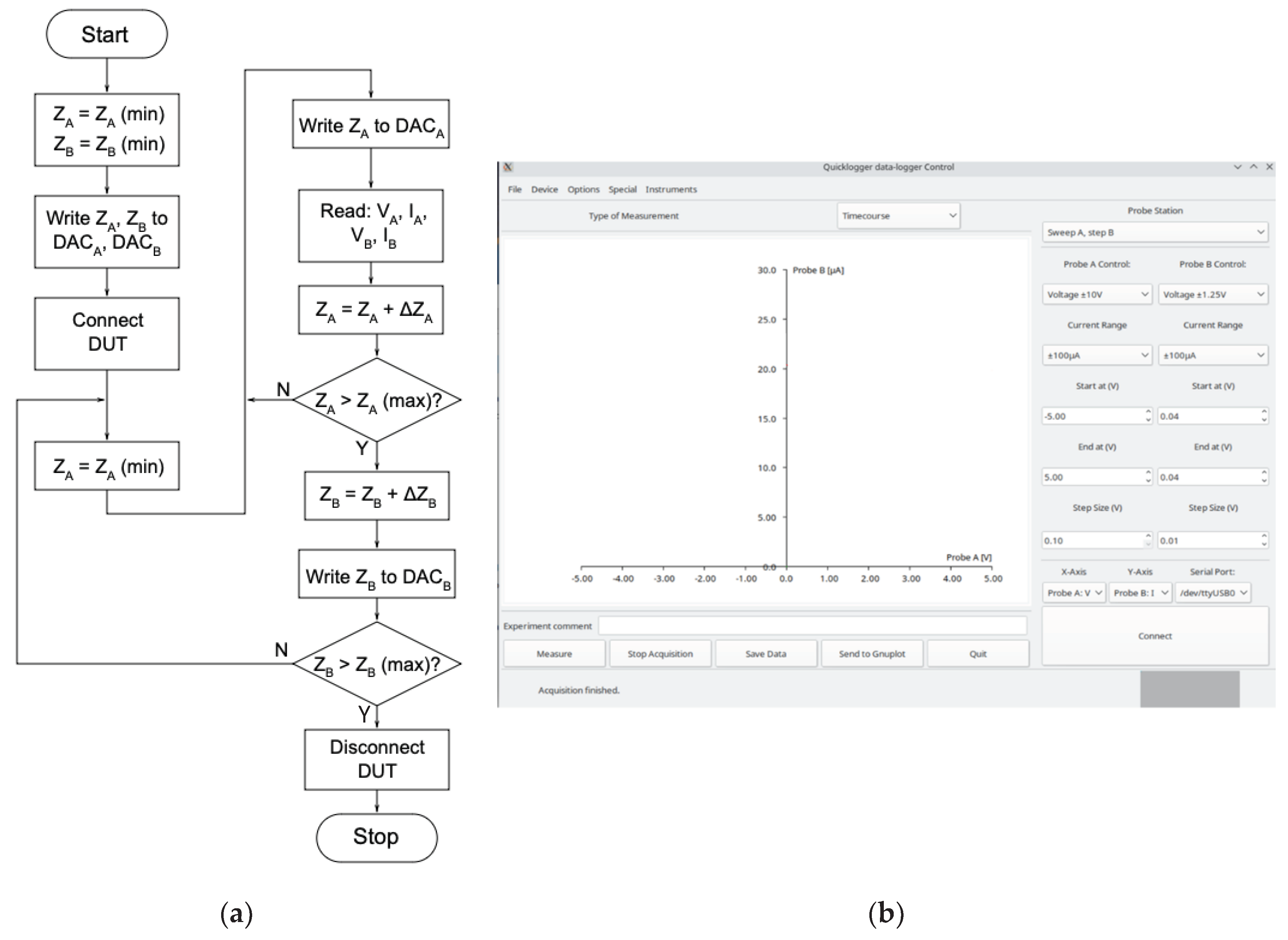
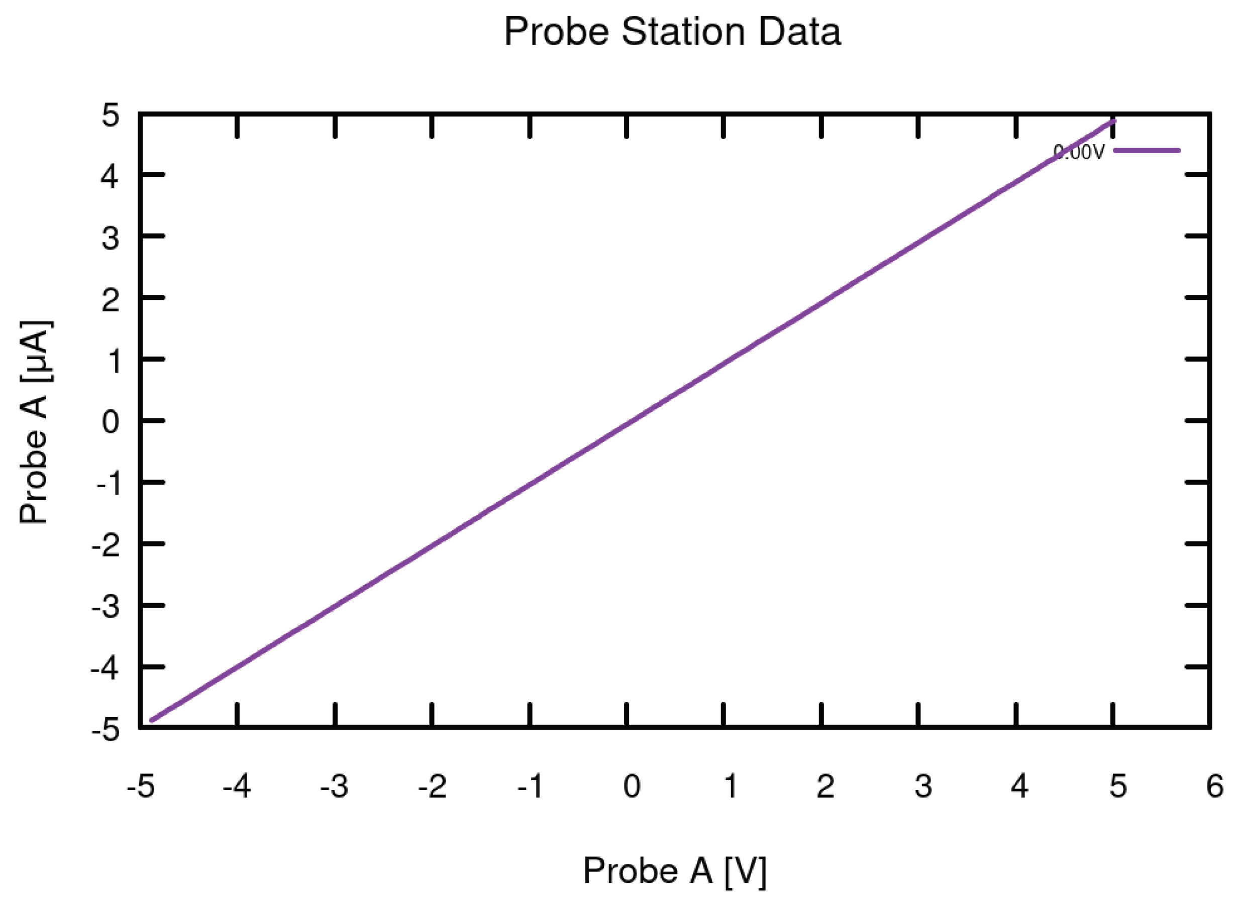
The basic function of acquiring V-I curves was first tested with standard electronic components with known responses. For semiconductors, the measaured response was cross-referenced with its datasheet containing the identified curve behavior. The first device used was a 1 MΩ resistor used to verify the calibration discussed in the previous section before investigating more complex components. The resistor was tested for Probe A and Probe B at each current and voltage mode: Voltage Mode 8/16 + Current Mode 1/3/5/7 for a total of 16 tests. In accordance with Ohm’s law, the expected response for each MΩ resistor test was a linear curve through the origin with a slope of 1. As exemplified in
Figure 6, when testing the 1 MΩ resistor across Probe A and GND for Mode 8 (Voltage control = +/- 10V) and Mode 5 (Current range = +/- 5 µA), a linear curve from -5V to 5V and -5 µA to 5 µA through the origin with a slope of 1 was the result, confirming data logger functionality and validating calibration. The same data was collected for the remaining modes and Probe B.
Based on the data collected for the 1 MΩ resistor in
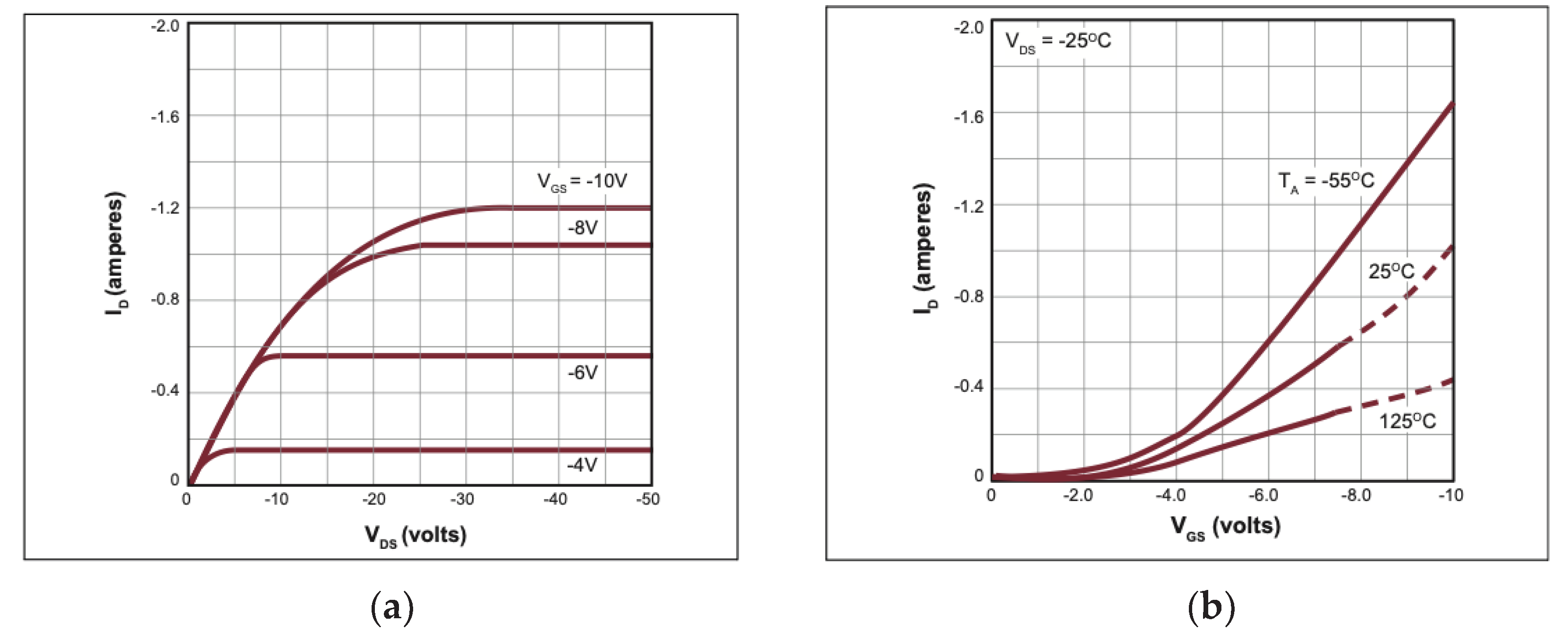
Figure 6, the signal-to-noise ratio (SNR) was calculated using the voltage and current values from Probe A. The SMU was proven to have an excellent SNR of about 63 dB, making it comparable to commercial devices on the market. After the 1 MΩ resistor testing confirmed that the SMU was functioning properly, active components were introduced to observe whether the device could accurately measure their expected output characteristics as well. The first device tested was the TP2540, a low-threshold p-channel enhancement-mode transistor with a vertical DMOS structure [
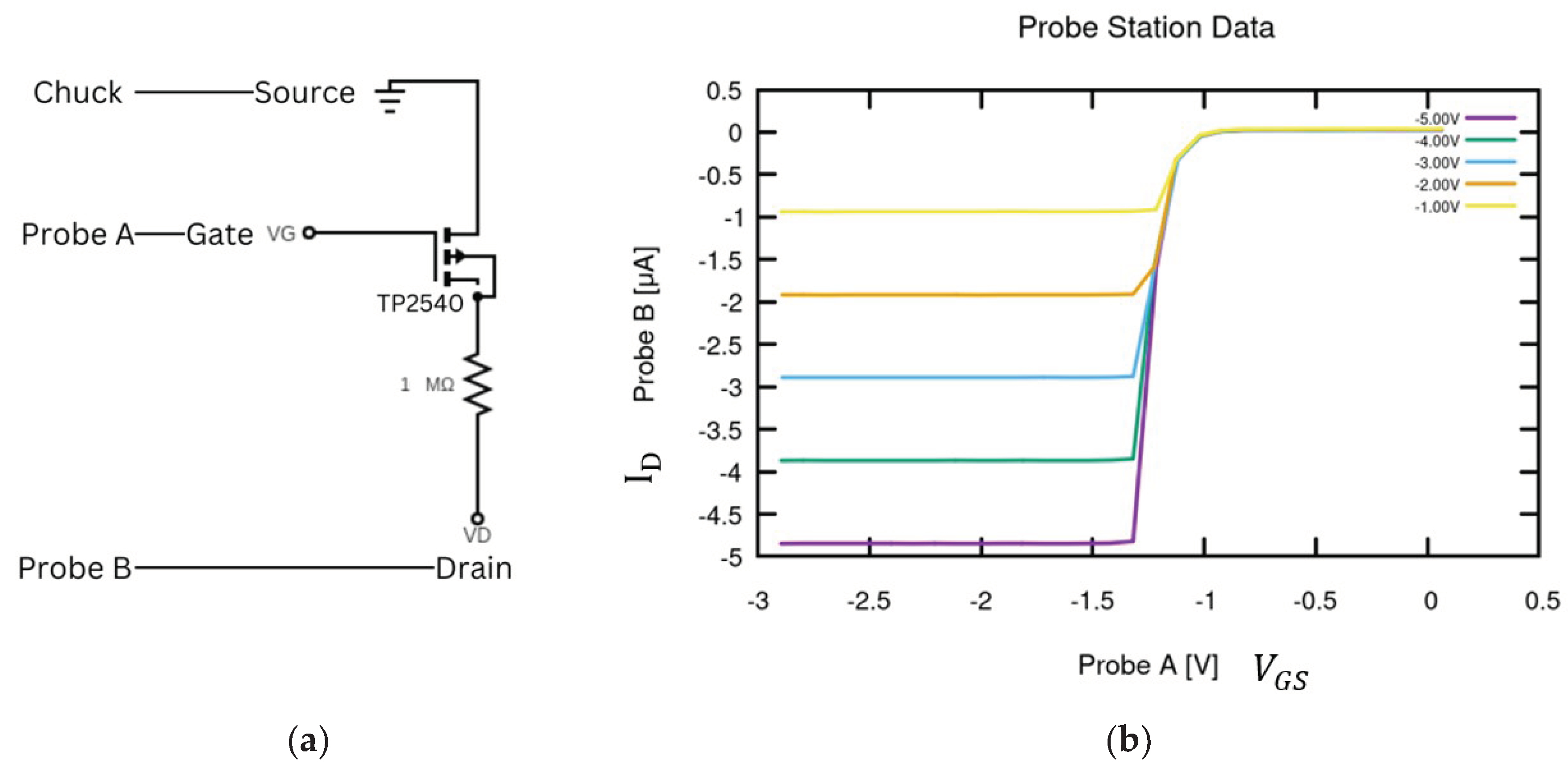
14]. This device is known for its high current carrying capacity; therefore, a 1 MΩ resistor was placed between the drain electrode and associated probe for data collection due to the SMU’s 100 µA maximum current range, specified for the target DUT. The effect of the resistor can be seen on the output curves, demonstrating the device’s sensitivity. The datasheet for this component was referenced to identify the general transfer characteristics for the device, as seen in
Figure 7.
The SMU was first used to confirm the
ID v
and
ID v
VDS curves for the TP2540. For the
ID v
VDS curves, the output characteristics were measured by looking at
ID across
VDS over various
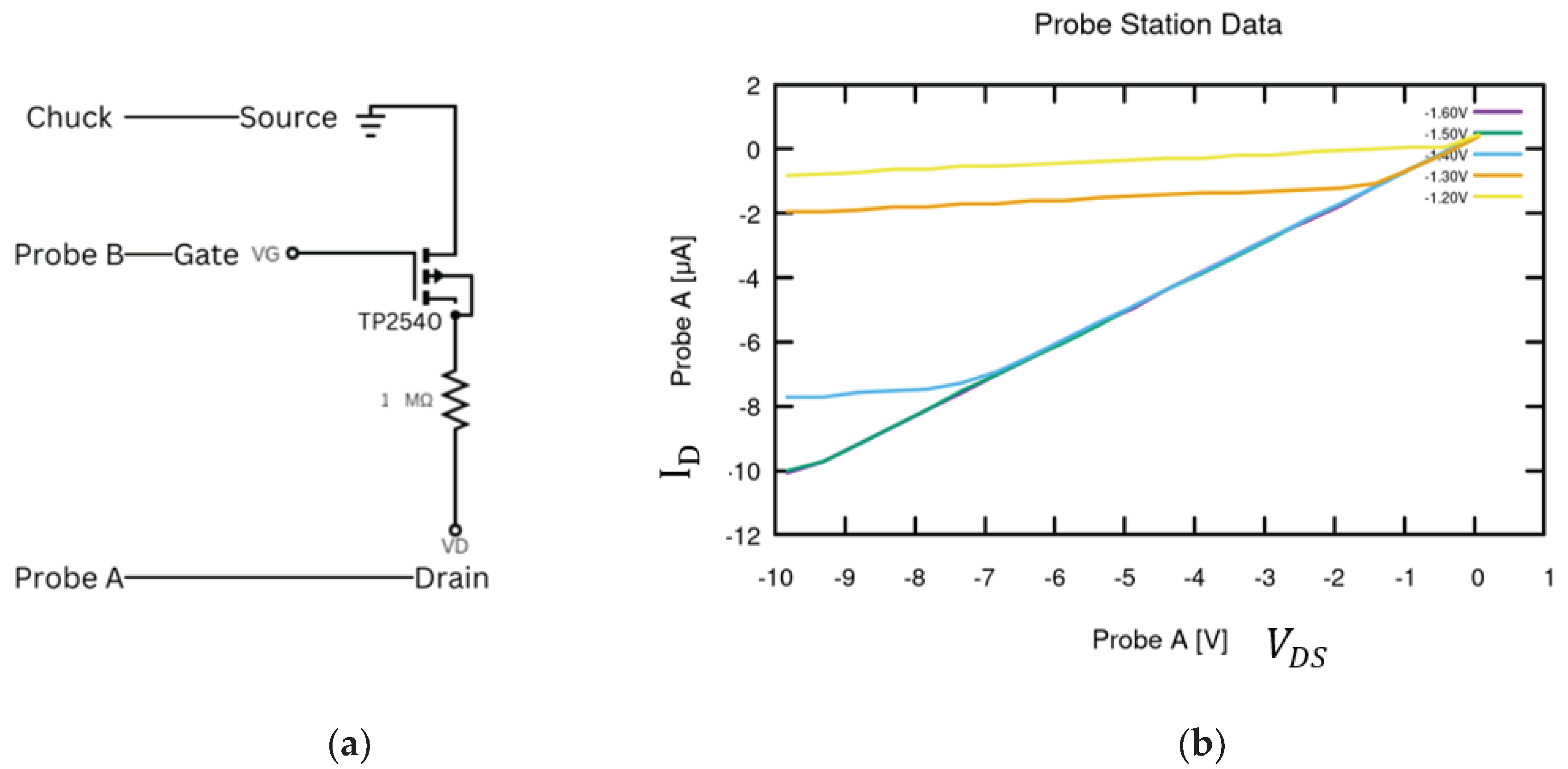
values. Probe A was connected to a 1 MΩ resistor then to the drain and set to Mode 8 for observation of
VDS from -10V to 0V and current range Mode 3, +/- 20 µA, the calculated range for the output response. As mentioned, the 1 MΩ resistor was used to decrease the overall current output so that it was in a range that the SMU was capable of measuring since the target DUT utilizes the µA range. Probe B was attached to the gate and set to Mode 8 to observe
at -1.6V, -1.5V, -1.4V, -1.3V and -1.2V, by inputting the voltage range as -1.6V to -1.2V with a step size of 0.1V. These
VDS values were selected in order to achieve this max current for testing device capability, and current range Mode 3 was again utilized. Probe A voltage (
VDS) was reflected on the x-axis and Probe A current (
ID) was reflected on the y-axis. As seen in
Figure 8, the device was able to accurately measure the
curves with the same overall behavior at lower current levels due to resistor impact.
Following the output characterization of the TP2540, the transfer characteristics were collected for the
ID v
curve, identified from the vertical cross section of the
ID v
VDS plot to ensure measurements were taken across adequate voltage ranges. Probe A was attached to the gate at Mode 8 to test from -3
to 0
, as selected from the
ID v
VDS curves, and Mode 5 for an expected current range of +/-5 µA. Probe B was attached to the 1 MΩ resistor for the discussed current suppression then to the drain at Mode 8 to test across -5
VDS to -1
VDS at 1V step size, with current range set to Mode 5. Probe A was set for the x-axis voltage (
), while Probe B was set for the y-axis current (
ID). As seen in
Figure 9, the effect of the resistor is prominent, as seen by the steep L-shaped bend in the
VDS curves. Without the presence of this additional resistance, the curves would continue to the maximum
ID the device is capable of measuring at +/- 100 µA, as observed by the datasheet. This confirms the device’s ability to accurately measure the
v
ID curve needed for future DUT data collection within programmed parameters. After testing both passive and active components with the SMU, device functionality at low resolution was confirmed across voltage and current modes; therefore, the next step prior to target DUT data collection was integrating the SMU with a probe station to confirm testing integrity with an open-face BJT IC, as described in the section below.
3.2. Source Measure Unit (SMU) and Probe Station Integration Testing
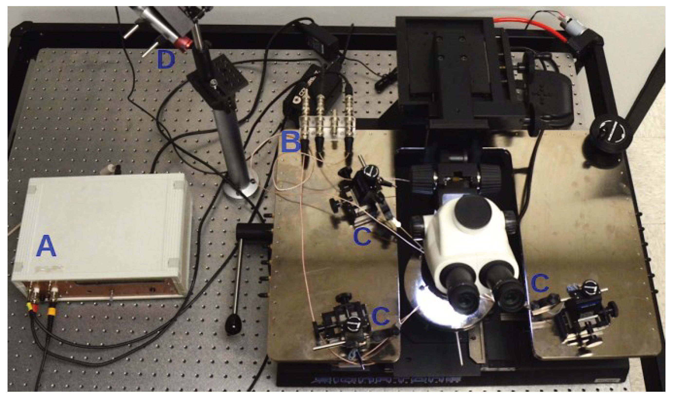
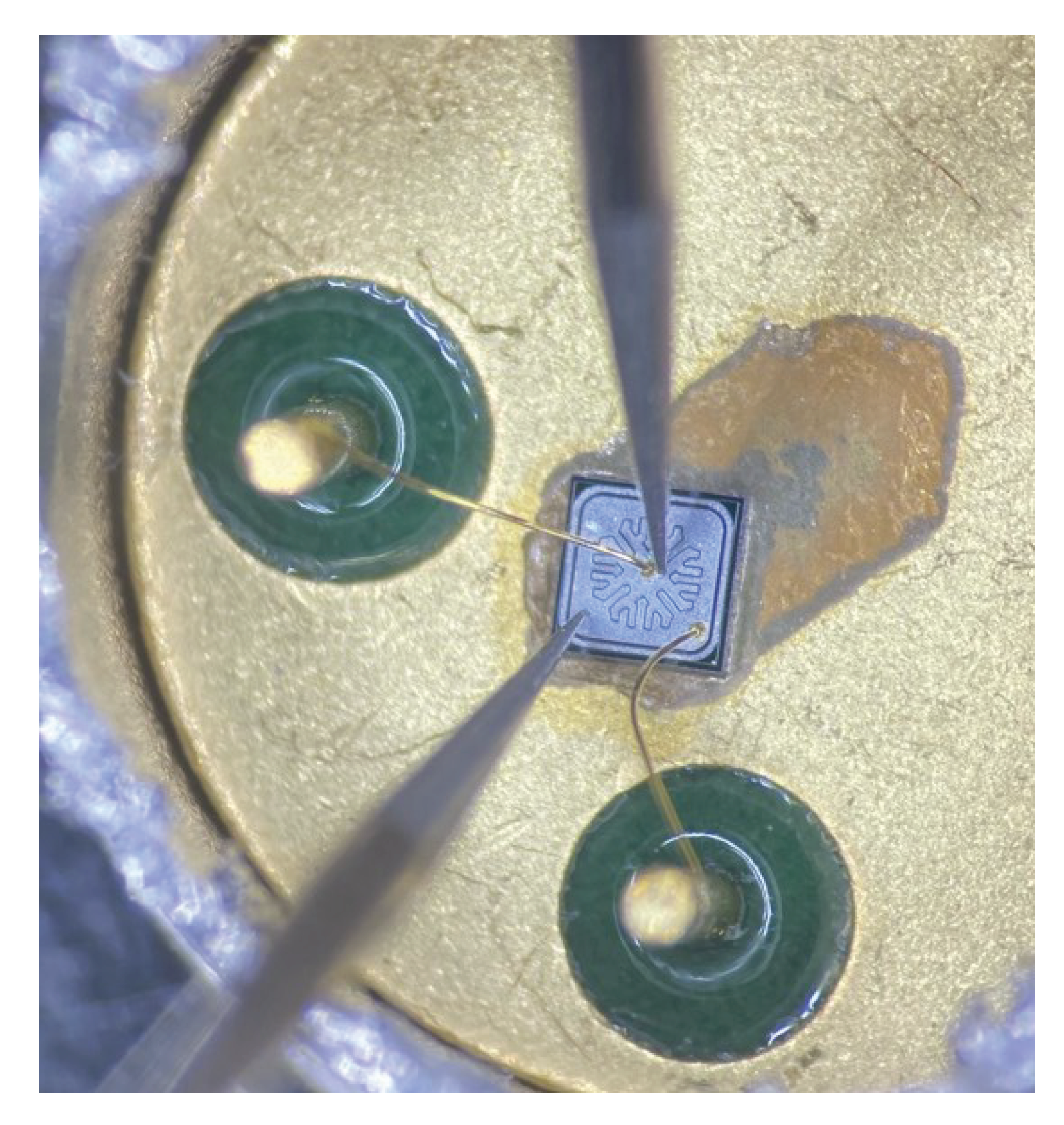
The SMU was integrated with a 3-point probe station using the BNC connection ports located on the probe station’s base in order to ensure the sensitivity of the SMU was still high when the probe station tungsten tips were used as the data collection points of contact rather than traditional cables. A bipolar junction transistor (BJT) IC was utilized as the DUT for this purpose, carefully sawing off the top of the protective shielding to be able to access the base and emitter terminals on the surface. Prior to testing, the exact device was unknown; however, the SMU was used to identify BJT behavior, with NPN vs PNP structure investigated below. The DUT can be seen in
Figure 10, the inside of the star-like shape is the emitter, the outside is the base, and the collector is the exterior of the device. For the test setup, one probe was allocated to the base and emitter terminals, with the final probe touching the probe station’s grounded chuck as the contact between the component and chuck with the SMU’s ground port allows for the collector to be assigned to GND.
Similar to the p-channel MOSFET testing, the first measurement carried out was the
v
ID curve, in this case the
v
curve, to gain insight of data collection points for the secondary curve measurements since the BJT operates by controlling the flow of current between the emitter and collector rather than source and drain. Another key difference is that the base is current-controlled rather than voltage-controlled seen with FETs as applying voltage across the base-emitter junction would weaken the built-in junction voltage in forward bias mode, eliminating the equilibrium between drift and diffusion currents; therefore, the base was set to current source mode to allow for the net flow of charge carriers across the BE junction to remain at zero [
15] and higher current gain.
For the
v
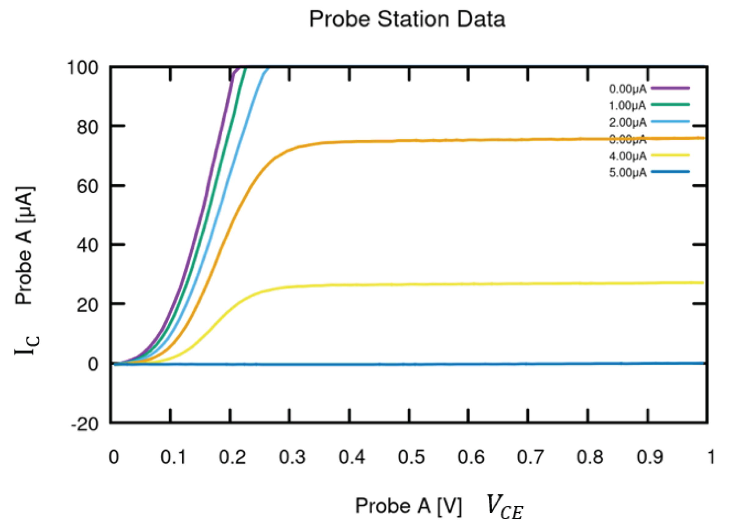
curve collection, the emitter terminal was connected to Probe A set to Mode 16 for +/-1.25V and Mode 1 for a current range of +/- 100 µA to capture the entire range of
curves generated at the following specified base currents. Probe B was connected to the base with Mode 1 also selected for the current range, but Mode 5 was selected for the source control to provide a base current of +/- 5 µA. To determine whether the device was a NPN or PNP BJT, negative values were first selected, keeping in mind the typical curve behavior of each type. The measured curves showed reverse polarity, resulting in the conclusion of a NPN structure as turning on a NPN BJT requires a base current that is more positive than the emitter with a positive voltage supply provided to collector rather than the PNP settings that were selected since NPN transistors use electrons as the majority charge carriers [
15]. With this in mind, the settings were adjusted to provide Probe A (emitter) with 0V to 1V and Probe B (base) with 0 µA to 5 µA at 1 µA steps, with GND remaining connected to the chuck (collector). Probe A was set for the x-axis voltage (
) and y-axis current (
).The resulting curve can be seen below in
Figure 11, with the saturation region seen at about <0.3
, active region at about 0.3V<
<0.8V, and cut-off region below the -1 µA curve.
It should be noted that the maximum SMU current is set to read 100 µA, based on mentioned DUT design specifications; therefore, the 0 µA - 2 µA curves are somewhat cut off past 0.15 , once entering the active region, and remaining curves would be better reflected with 0.5 µA current steps. However, overall the BJT IC has similar low signal emission at lower base currents (-3 µA and -4 µA) to the target DUT, making it a great choice for SMU sensitivity testing at these values. Taking the vertical cross section of the curves would result in the corresponding v curve.
3.3. Quality Testing: Accidental Schottky Junction Formed by Oxide Breakdown
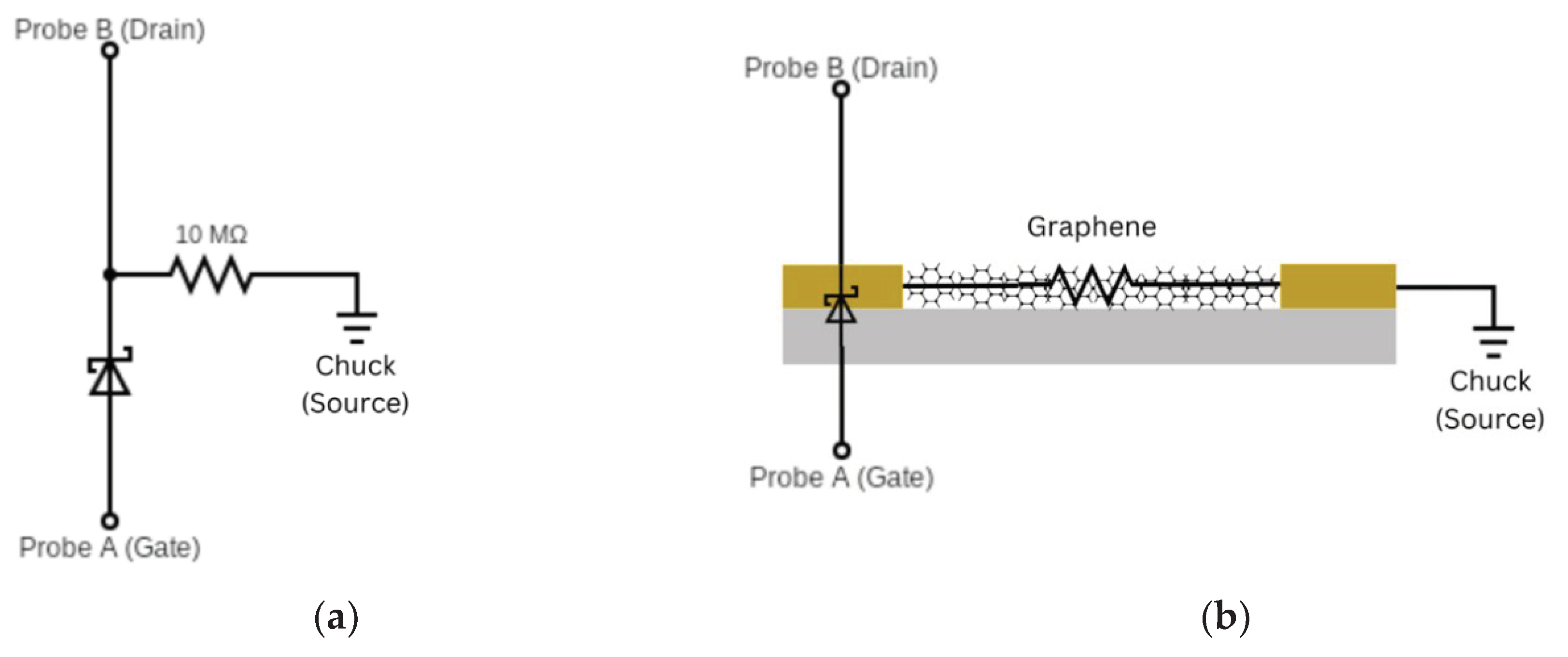
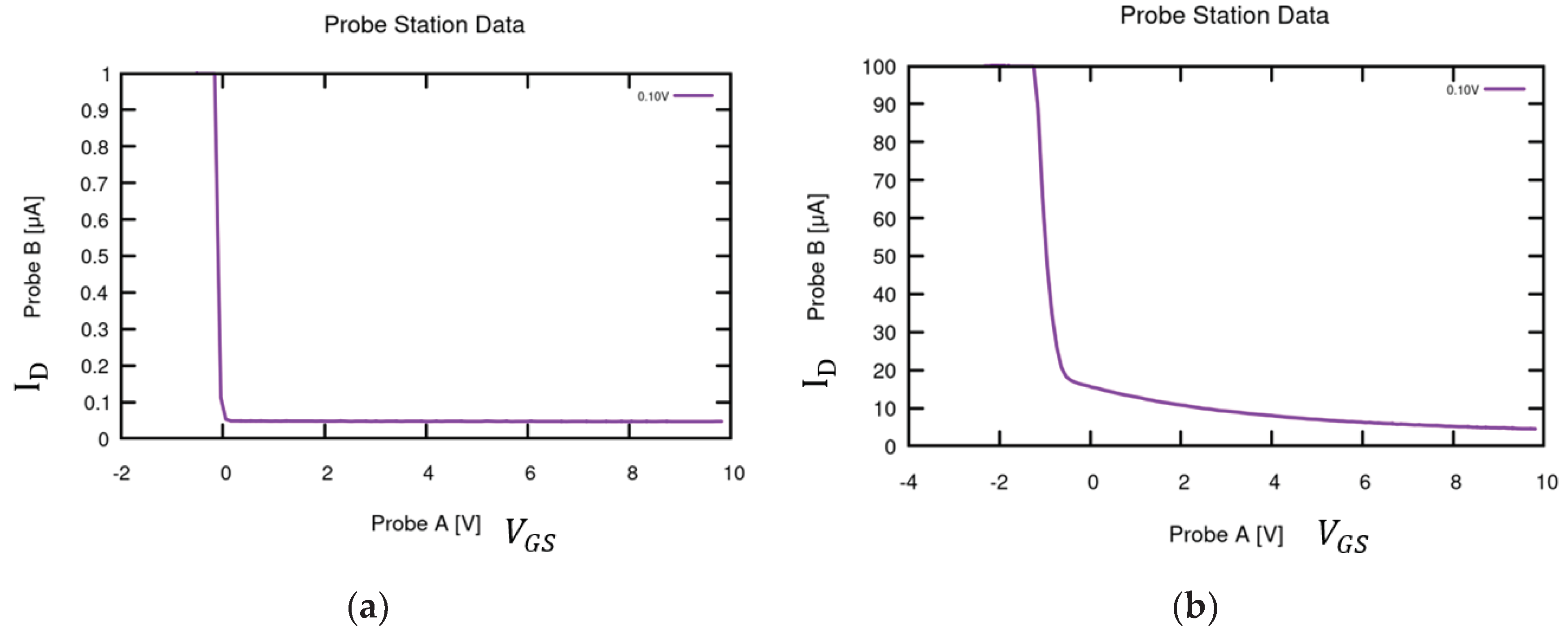
Another example prior to testing the target DUT was a quality check to see if the device was capable of picking up errors with the graphene-FET structure. The DUT has metal source and drain electrodes on its surface with a metal back gate located underneath the insulating oxide layer. If the oxide layer were to be compromised, this would result in the metal source/drain electrodes to be in contact with the metal gate electrode creating a Schottky junction. The oxide could be compromised as a result of a fabrication error, probe punctures, or too high of a current through the gate channel; therefore, by testing the expected response for the Schottky junction, errors during DUT testing could be better diagnosed. The schematics for each can be seen in
Figure 12.
For the Schottky diode and resistor test, the gate was connected to Probe A and voltage Mode 8 from -10V to 10V at current Mode 7 (1 µA) with the Schottky diode in reverse polarity. The drain was connected to Probe B at voltage Mode 16 with a constant 0.1V and current Mode 7. As seen in the schematic, a 10 MΩ resistor was connected across drain and source, which was connected to GND through the probe station chuck in order to maintain a current in a range capable of device measurement and component parameters at 1 µA. Probe A was set for the x-axis voltage (
), while Probe B was set for the y-axis current (
ID). The expected response can be seen in
Figure 13a. The diode drains the current to the gate driver; the horizontal line shows the current through the resistor, and when the voltage is negative
ID shoots up the reach the current level that the gate is driving. The key insight provided by the test setup is that the diode conducts earlier than 0.7V much like the silicon of the target DUT back gate due to the exponential relationship between the diode voltage and current.
After the test was completed, it could be compared to a defect on one of the target DUT sensors, whose surface was punctured during a step of the fabrication process. The test setup above was replicated – gate was connected to Probe A and voltage Mode 8 from -10V to 10V at current Mode 7 (1 µA). The drain was connected to Probe B at voltage Mode 16 with a constant 0.1V and current Mode 7. The oxide breach was located on the drain electrode, as seen on the schematic in
Figure 12(b), and the source electrode was connected to GND through the probe station chuck. Probe A was set for the x-axis voltage (
), while Probe B was set for the y-axis current (
ID). The
expected response can be seen in
Figure 13(b). The curve shows the current shooting up right before the 0
mark seen during the test setup and drop down to ~0 µA by 10
. Now that device quality testing is complete, evaluating the target DUT is the next step.
3.4. Target DUT Testing
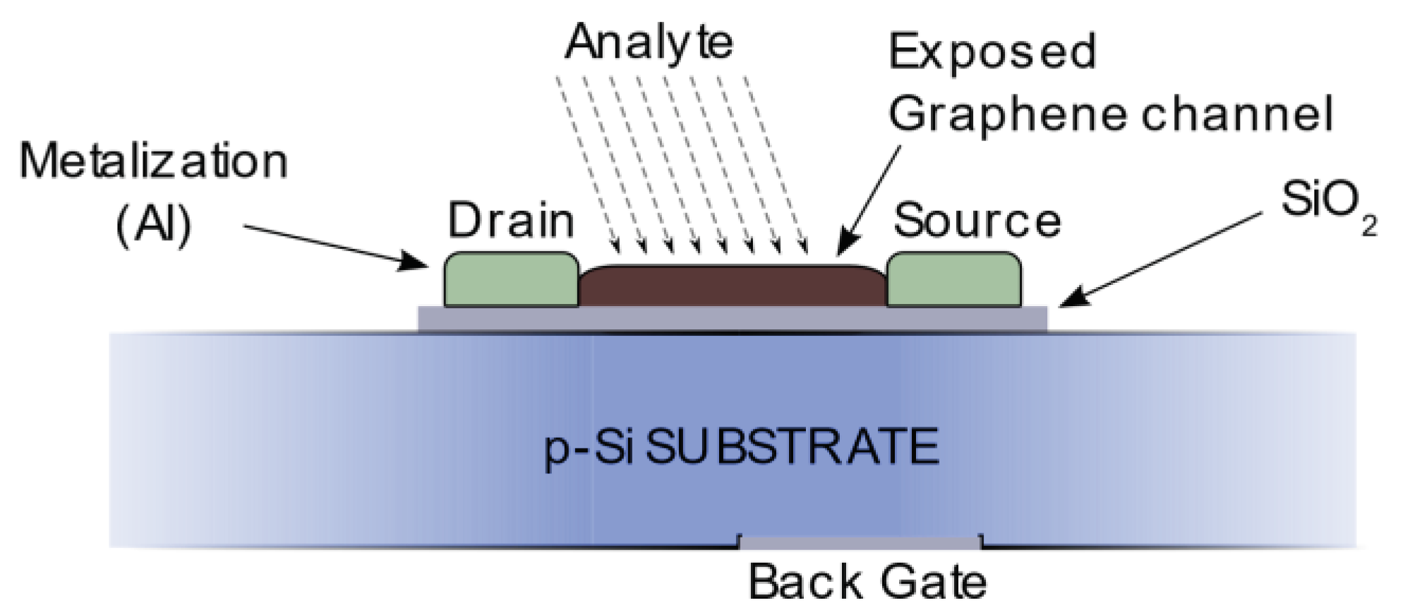
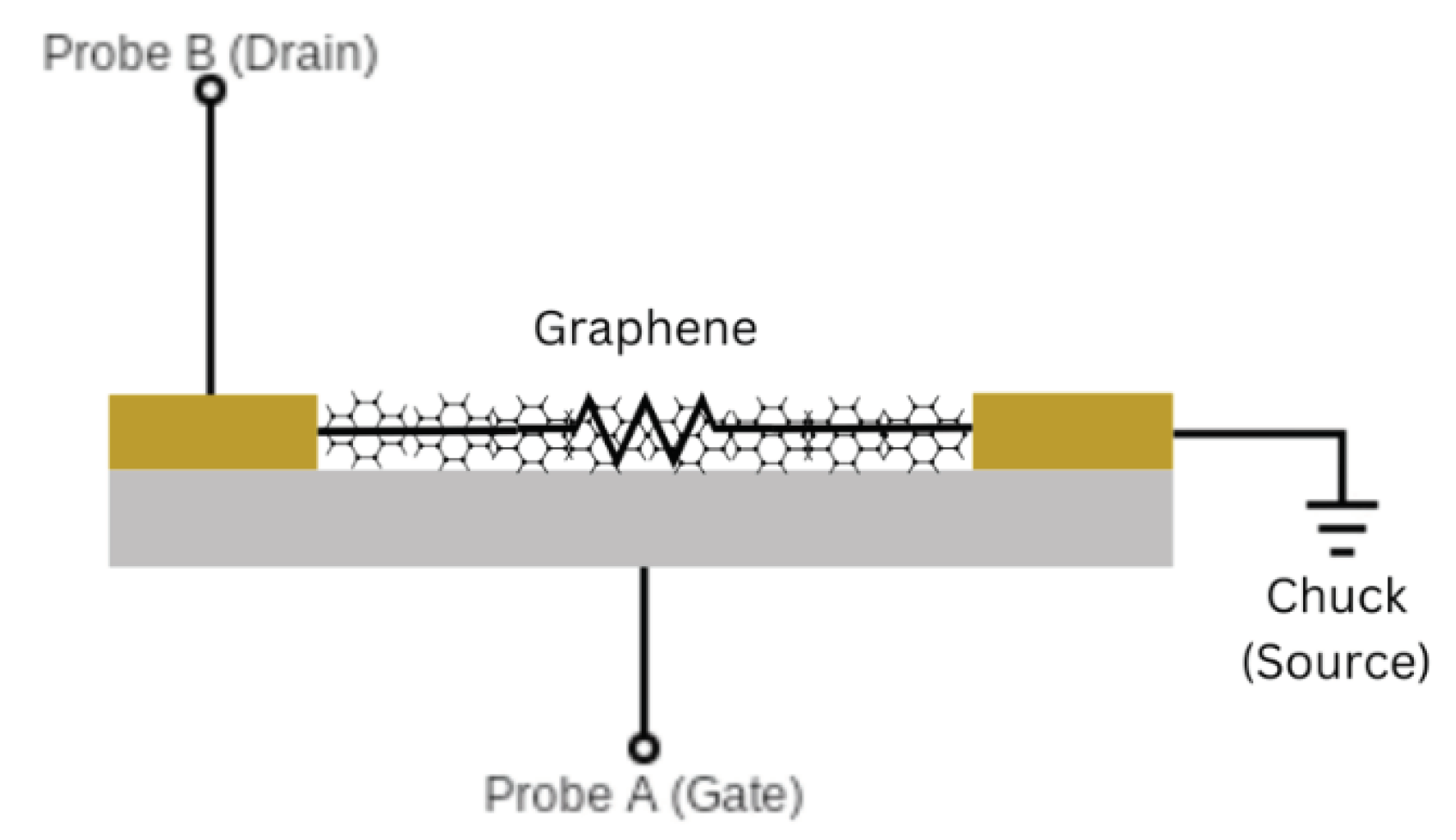
The graphene FET used as the target DUT was created using a p-doped silicon substrate with a thin oxide layer and gold source/drain electrodes on the sensor surface. The device has a back gate structure with a thin gold layer on top of the silicon serving as the gate and graphene across source and drain electrodes serving as the gate channel. The G-FET schematic can be seen in
Figure 14.
As discussed, graphene FETs have ambipolar behavior in which holes are majority carriers in the negative
region while electrons are majority carriers in the positive
region. The expected
curve is therefore a U-shape with the Dirac point located at the lowest
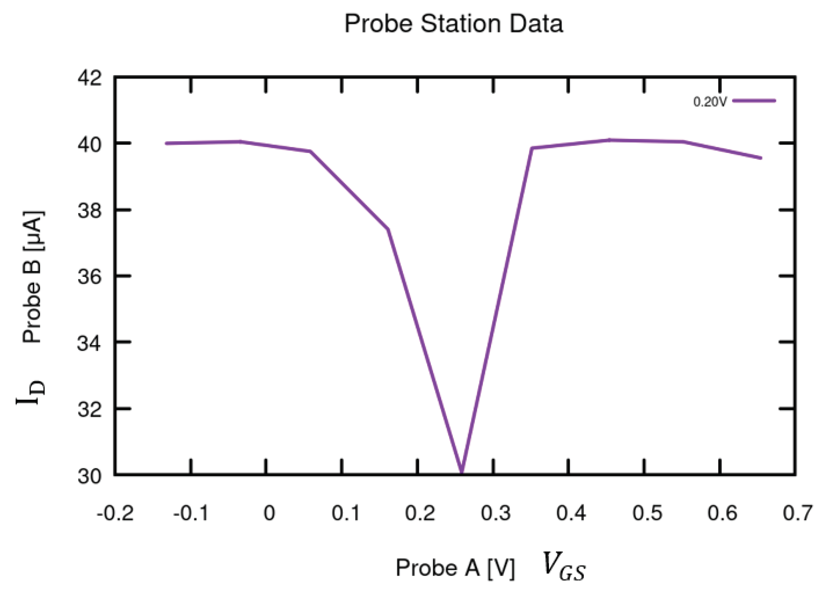
ID. In order to test the expected
v
ID curve, the gate was connected to Probe A and voltage Mode 8 from -0.2V to 0.7V at current Mode 1 (100 µA) by placing the device on the probed chuck. The drain was connected to Probe B at voltage Mode 16 with a constant 0.2V and current Mode 1. Probe A was set for the x-axis voltage (
), while Probe B was set for the y-axis current (
ID). The expected response can be seen in
Figure 15, the Dirac point is located at ~0.25
at ~30 µA
ID. As discussed in the G-FET challenges, the ultra-sensitive nanoscale surface is reflecting noise caused by the uncontrollable nature of the graphene itself; however, the overall curve behavior remains [
13].
Photodetection is a key research area for improvement of FET optical sensing applications. Improvement of the sensing mechanism for these devices would allow for optical communication, remote sensing, spectrum analysis, biomedical imaging [
16]. Researchers have investigated the transfer characteristic curves generated by photodetection on the G-FET surface, specifically that excitons are generated in graphene under various light conditions with response intensity influenced by symmetry in design and the wavelength of light source. These excitons are separated to electrons and holes near source and drain electrodes as a result of their corresponding electric fields [
17]. For the design of the target DUT discussed here, the graphene was deposited closer to the source electrode, thus resulting in asymmetric behavior on the
v
ID curve when compared to the control in
Figure 15. This is due to the photovoltaic effect which generates increased photocurrents compared to a gate channel with symmetric orientation [
17] at the site of asymmetry. Since the graphene is deposited closer to the source, the negative gate bias generated a stronger drain current and ambipolar response is no longer observed as the positive gate bias does not have an increased photocurrent. This leads to the conclusion that holes are the majority carriers present and reflected on the curve due to their relationship with the negative gate bias.
For testing, the same probe connections and test setup used for the control G-FET
v
ID curve discussed above; however, a different device was used for repeatability purposes; therefore, a separate control
v
ID curve was collected prior to laser illumination. Similar to the
v
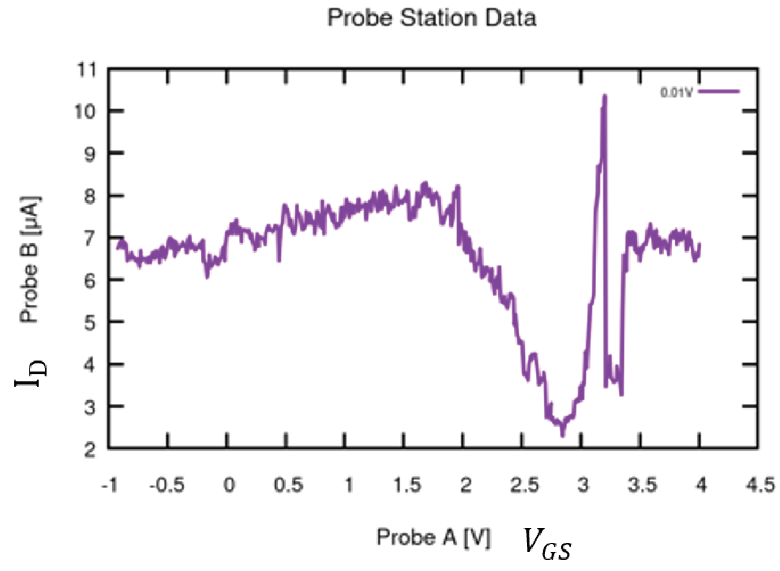
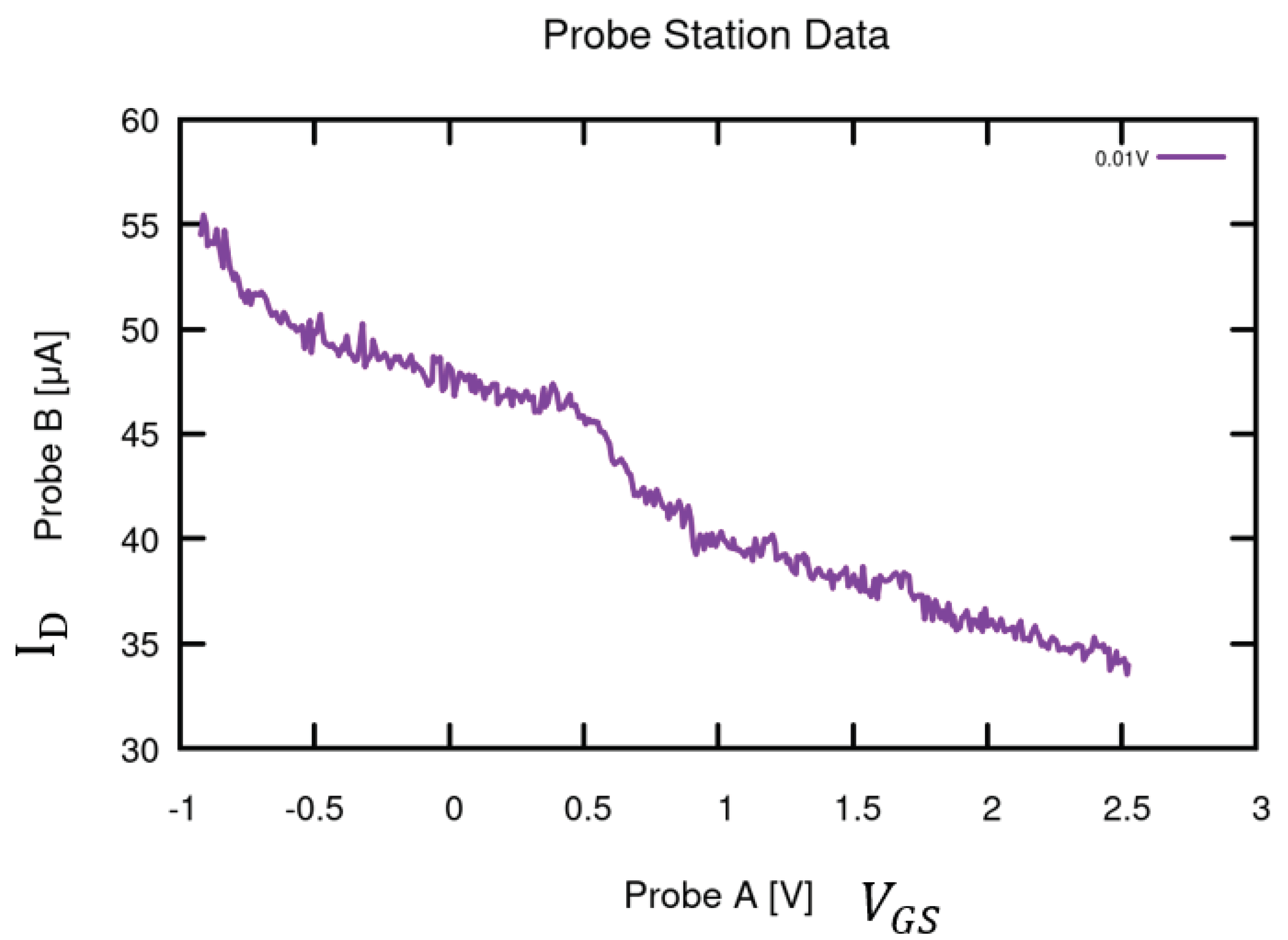
ID testing above, the gate was connected to Probe A and voltage Mode 8 from -1V to 4V at current Mode 1 (100 µA) by placing the device on the probed chuck. The drain was connected to Probe B at voltage Mode 16 with a constant 0.01V and current Mode 1. Probe A was set for the x-axis voltage (
), while Probe B was set for the y-axis current (
ID). The expected response can be seen in
Figure 16, the Dirac point is located at ~2.8
at ~2.3 µA
ID. The curve reveals that different devices have different responses, required
VDS, and noise presence based on the orientation and concentration of graphene in the gate channel. The Dirac point for this device in comparison to the first decreases by over 28 µA and is shifted to the right by over 2.5V.
Once the control curve for this device was collected, a 632nm, 0 - 10mW solid-state laser (Coherent LabLaser series, Coherent Corp., Saxonburg, PA, USA) was used and pointed at the surface of the device angled ~45°. The gate was connected to Probe A and voltage Mode 8 from -1V to 2.5V at current Mode 1 (100 µA) by placing the device on the probed chuck. The drain was connected to Probe B at voltage Mode 16 with a constant 0.01V and current Mode 1. Probe A was set for the x-axis voltage (
), while Probe B was set for the y-axis current (
ID). The expected response can be seen in
Figure 17, the Dirac point is not as present due to the asymmetric gate channel; however, the curve seems to have a sharp decline at ~0.5
with similar noise present due to the sensitivity challenges of the G-FET itself. Additionally, the increase in
ID is extremely prominent in comparison to the control response, shifting upwards by ~48 µA due to electron excitation.
The
VDS v
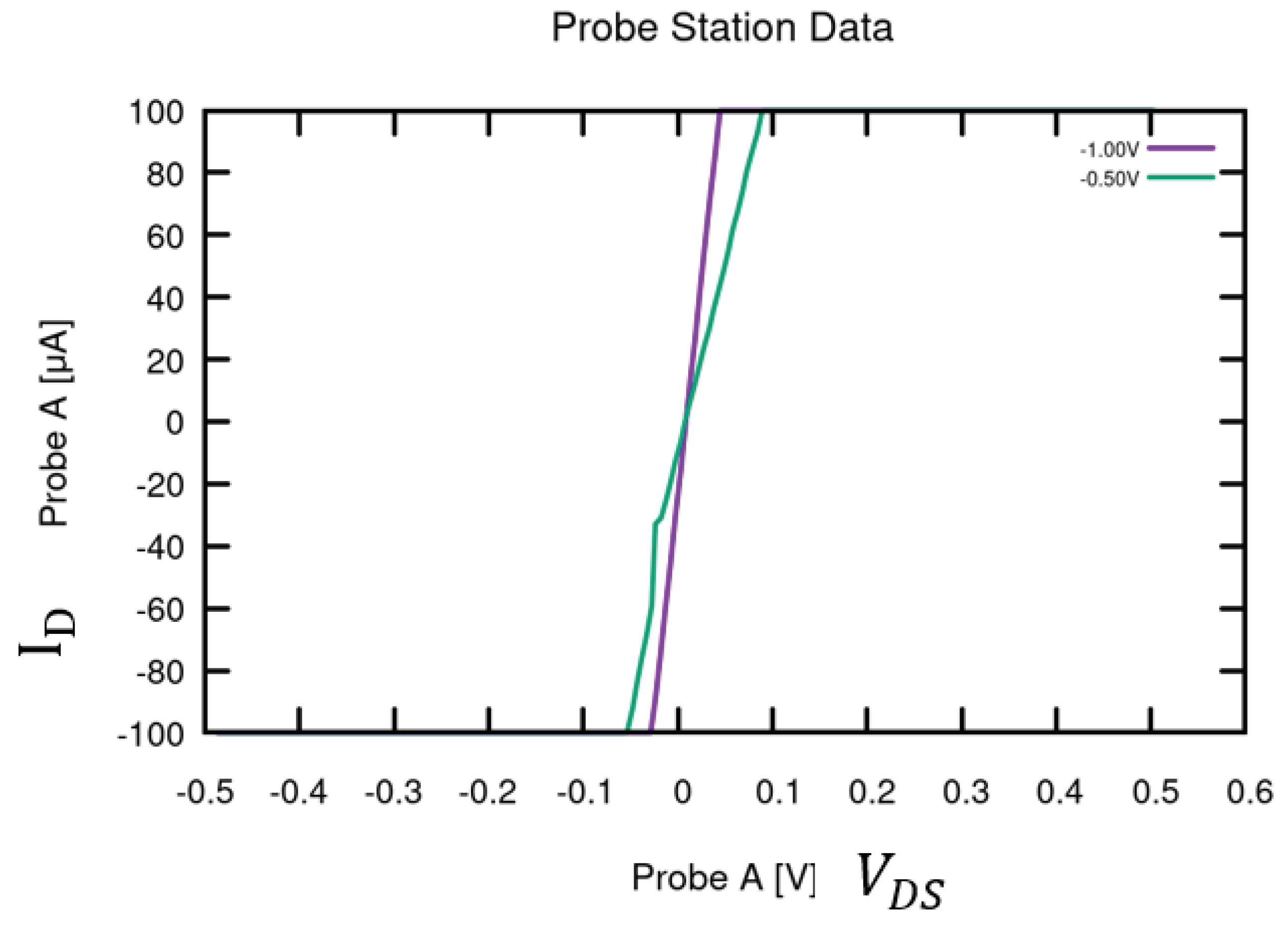
ID curve was collected next with the drain connected to Probe A and voltage Mode 16 from -1V to 0.5V and 0.5V steps at current Mode 1 (100 µA). The gate was connected to Probe B at voltage Mode 16 with from -0.5V to 0.5V and current Mode 1. Probe A was set for the x-axis voltage (
VDS) and y-axis current (
ID). The expected response can be seen in
Figure 18, with variation between curves at about a 0.05V range. Due to the ultra-sensitivity of the device, challenges were presented in the data collection; however, with increased
, the curves should continue to decrease then begin to increase again after passing the
value associated with the Dirac point.
