1. Introduction
The boost converter is commonly used in active power factor correction (PFC) applications. With AC line voltage at the input and even higher DC output, providing a reliable low voltage bias power for the control circuitry of the converter is an engineering challenge that is often underestimated.
The application of a dedicated housekeeping power supply is a proper, however, costly option to derive the required low-level DC voltage. Yet, the obvious advantages of such an approach are that the design is theoretically solid and practically robust.
The first that may come to mind when facing the problem of bias circuit design is the application of a buck converter. Especially in case the control board is large and requires relatively high power. However, a simple buck is not up to the job. The steep step-down conversion ratio requires the basic buck converter to operate at an extremely narrow duty cycle that impairs the converter’s efficiency. Instead, a buck-derived topology such as [
1] or like should be considered. The buck converter can also provide multiple bias voltages [
2]. Yet, buck-derived converters require costly high-voltage switches and floating drivers. Besides, the controller circuitry of the buck converter also demands power - this may bring the designer back to the starting point.
A flyback converter is an alternative solution for biasing relatively large control boards [
3]. Flyback can provide both isolation and regulation of the auxiliary output and has a single grounded switch that is easy to drive. Also, a well-designed transformer’s turn ratio allows for operating at a moderate duty cycle at the point of optimal efficiency. Moreover, multiple outputs can be easily configured, one of which can provide self-bias for the flyback controller. The disadvantages of the flyback converter are the extra high voltage stress of the main switch and the need for snubber circuitry to suppress the ringing caused by the leakage inductance of the transformer. Alternatively, a single switch cascaded buck-boost converter can be employed [
4]. When fed from the main regulated output such a converter can be operated in the open loop in the discontinuous conduction mode and requires neither feedback nor compensator networks, and, thus, is simple to design and implement. Since the topology is transformless, it is less noisy than a flyback converter. A rather complex topology of a unity power factor auxiliary power supply based on a self-oscillating flyback and two forward stages with multiple outputs was proposed in [
5].
Yet, the available off-the-shelf ICs that incorporate an integrated high-voltage main switch and a current mode controller [
6] or alike may present a more attractive proposition for implementing a flyback-based auxiliary power supply than a home-breed circuit.
However, providing a dedicated auxiliary power supply can be considered only for top-of-the-line products, as such an approach is impractical in applications where the controller consists of just a couple of ICs and the cost is at a premium. Therefore, several engineering solutions were developed to self-bias simple low-power controller circuits.
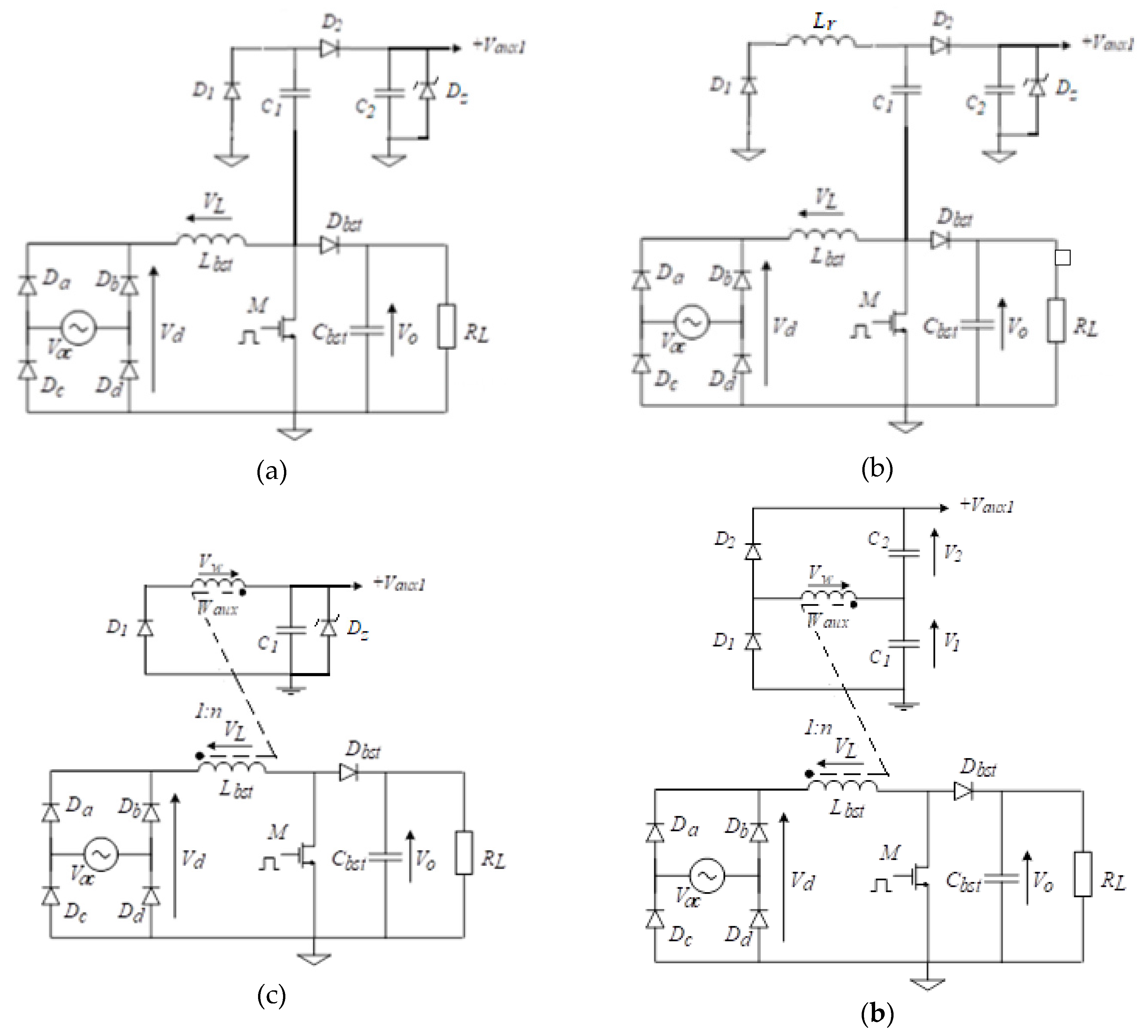
A popular cost-effective solution to bias a single controller IC is by using a charge pump driven by the main switch [
7], see
Figure 1a. Here, when the boost switch is turned off the charge pump capacitor is charged to the
and so acquires a charge
. The same charge is deposited on the much larger capacitor,
, which is charged in series, via
. The average current provided by the charge pump depends on the switching frequency,
, and equals
. Therefore, the charge pump acts as a current source. The excess current (unused by the controller) is dumped into the Zener diode, which also regulates the voltage of the bias circuit. Note that, when the main switch is turned on
is discharged to zero through
. Thus, the stored energy is wasted to heat. The disadvantages of the charge pump approach are the lack of isolation and some additional power loss.
An interesting circuit, reported earlier as a lossless snubber for Forward [
8] and Flyback converters [
9], can be designed to recover energy into an auxiliary supply [
10], or used with the sole purpose of providing power for the controller IC [
11], see
Figure 1b. When operated as a bias circuit, as the main switch is turned off the capacitors
and
are recharged via
. When the switch is turned on the capacitor
first resonates with the inductor
via
and transfers all of the stored energy to the inductor. Then the inductor releases the captured energy to the
via both
and
till the inductive energy is completely discharged into
. Hence, a nearly lossless operation is obtained except for the negligible switch and diodes’ conduction losses. The disadvantage of the circuit is that the delivered power depends on the operational conditions and may be either insufficient or excessive. Therefore, similarly to the simple charge pump case, a Zener diode regulator is needed to stabilize the voltage.
Another option for generating isolated bias power is by using an auxiliary winding coupled to the main inductor and a half-wave rectifier [
2,
6]. This approach works well with the buck, buck-boost, and flyback converters since the regulated output voltage appears across the main inductor during the off time. Thus, the auxiliary output is inherently regulated. Another advantage is that the circuit has voltage source characteristics. However, when applied to the boost converter, see
Figure 1c, the circuit loses regulation. This is because the inductor’s voltage in boost converters during the on-time equals the input voltage,
, whereas during the off time equals the difference between the output and the input voltages
, so that in either case it is strongly dependent on the varying input voltage. The problem is especially acute in the case of the PFC rectifiers, where the input voltage swings in a wide range. The circuit can still do the job [
12], yet requires a larger filter capacitor to support the voltage during the dips of the line and minimize the voltage ripple at the output of the bias circuit.
A more interesting solution, based on a voltage doubler rectifier, was shown to provide a stable bias voltage utilizing an auxiliary winding on the PFC boost’s inductor [
13,
14,
15], see
Figure 1d. The idea behind the circuit is that the capacitor
is charged to
, during switch’s on time, whereas the capacitor
is charged to
, during the switch’s off time. Thus, the sum
is independent of
and follows the regulated output voltage,
, which is well stabilized.
Worth noting that typically, to initiate the system’s start-up the filter capacitor across the V
aux is pre-charged via a very large start-up resistor connected to the line rectifier’s output and so provides the minimal voltage for the controller IC to kick in. To alleviate the power loss across the start-up resistor during the normal operation an active start-up circuit can be employed [
16].
This paper presents an alternative solution to deriving the bias voltage from the boost converter. The idea is hinged on the application of a charge pump circuit. The resulting bias circuit is passive and can provide self-regulated isolated output. Herein, the analysis of the circuit is reported and design guidelines are outlined. The theoretical expectations are verified by simulation and experimental results. The proposed coupled inductor-driven charge pump bias circuit has an advantage over the earlier doubler rectifier approach in that it can be modified to generate multiple and bipolar auxiliary bias outputs using single auxiliary winding.
2. Coupled Inductor Driven Charge Pump Bias Circuit
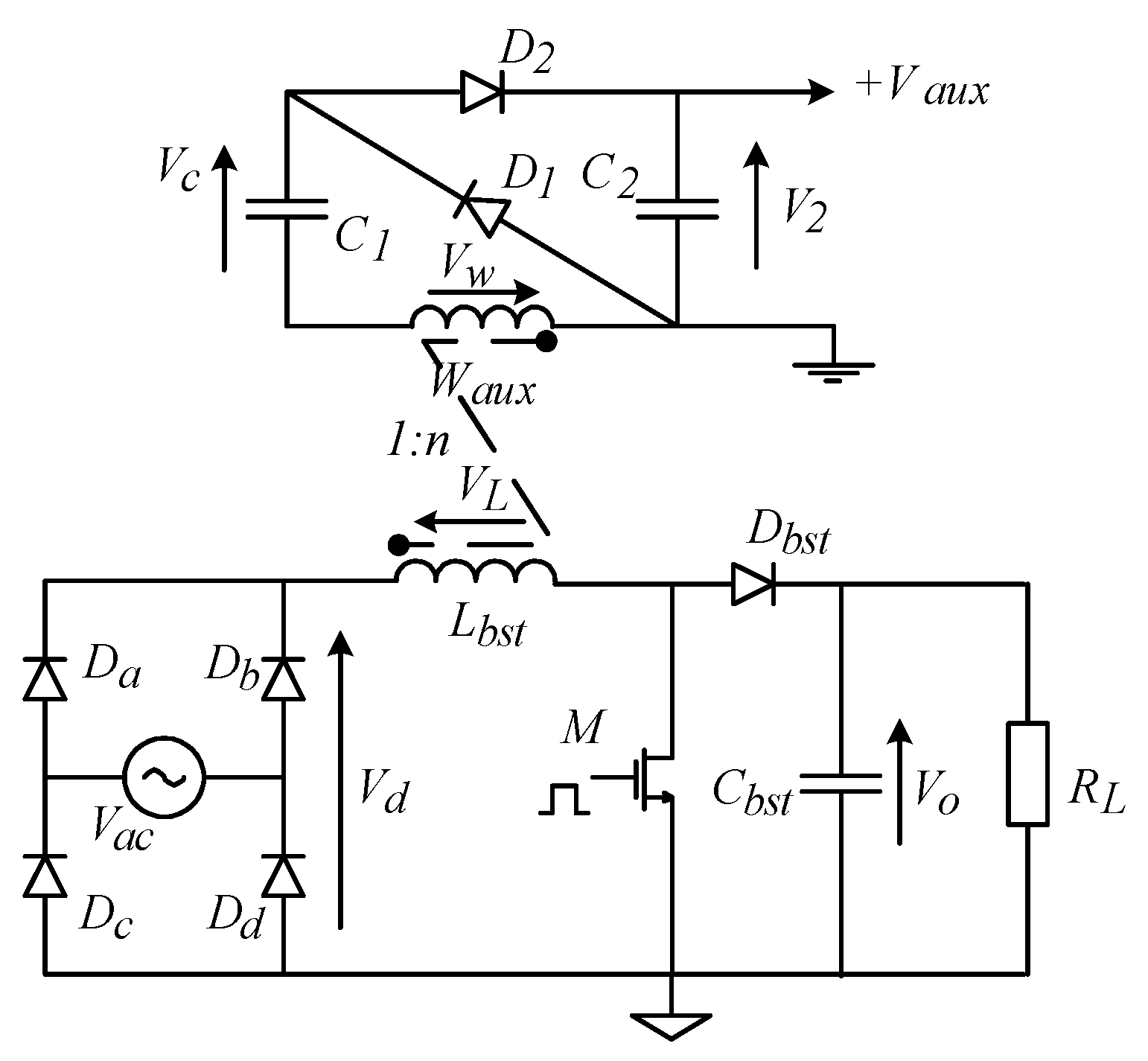
Boost PFC rectifier with a single output positive bias circuit is illustrated in
Figure 2. The power stage of the PFC rectifier consists of a full wave rectifier
, an active switch
, a boost output diode
, a boost inductor
, an output filter capacitor
, and an equivalent load resistance
. The proposed bias circuit constitutes a coupled inductor-driven charge pump (CICP). The CICP is comprised of a charge pump capacitor
, the output filter capacitor
, and a pair of diodes
,
. The auxiliary winding,
, is driving the charge pump and is coupled to the main inductor having
turn ratio.
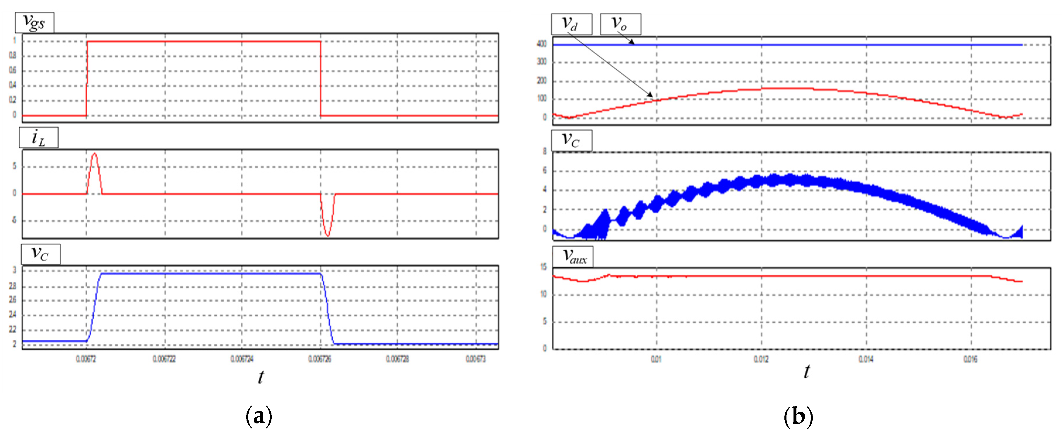
Operation of the boost power stage is only marginally affected by the addition of CICP. Hence, only the bias circuit will be modeled and described. Worth noting, that CICP works identically with the boost stage in either continuous or discontinuous conduction mode. Typical time domain waveforms of the CICP are illustrated in
Figure 3.
In the analysis to follow it is assumed that the auxiliary output filter capacitor is much larger than the charge pump capacitor,
, and therefore can be substituted by an equivalent voltage source,
. It is also assumed that a certain reflected equivalent leakage inductance,
, is present at the auxiliary winding. The leakage inductance dominates the parasitic resistances; therefore, the latter are neglected, while the diode’s voltage drop,
, will be accounted for. The analysis is performed by applying the state plane approach, a brief review of which can be found in [
17].
In the steady state, when the power switch,
, is turned on by the controller the voltage across the boost inductor equals the rectified line voltage,
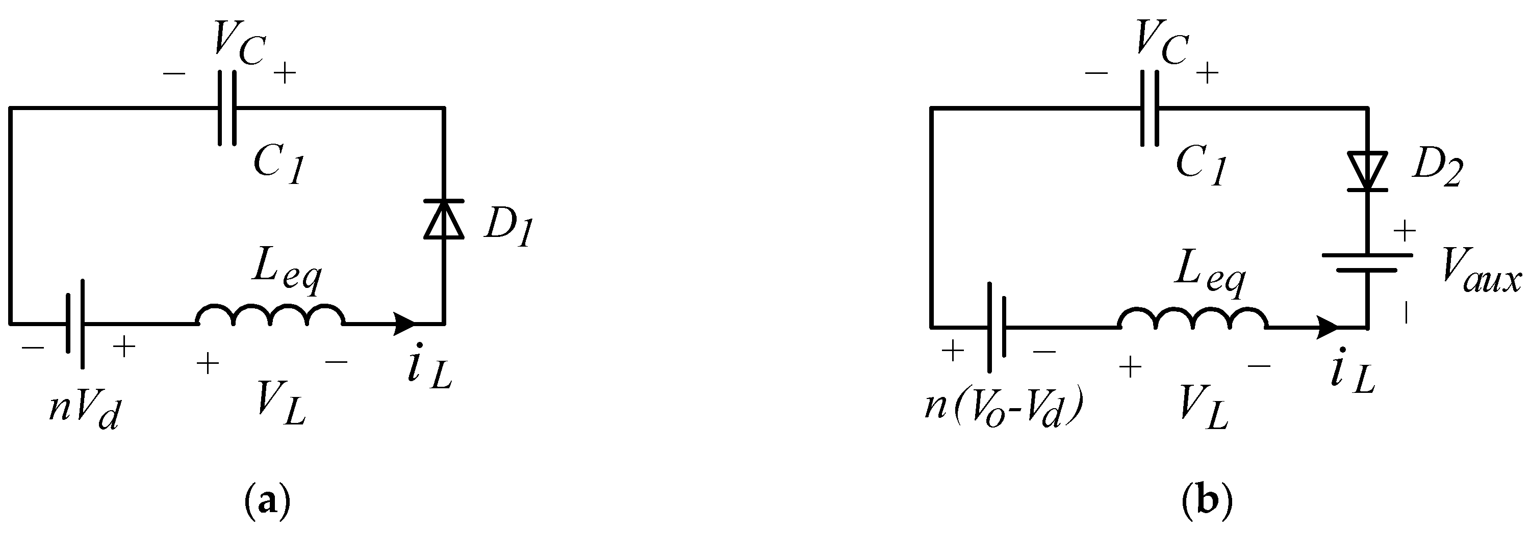
. During this interval the voltage induced in the auxiliary winding initiates a resonant current pulse in the charge pump circuit, see the equivalent circuit in
Figure 4a. Here, the capacitor
gets charged through the equivalent leakage inductance,
, and
. Accounting for the turn ratio,
, and the diode voltage drop,
, the voltage applied to the resonant tank, formed by
and
, is
When the power switch
is turned off the main inductor,
, starts discharging to the output and the voltage across it equals the difference of the rectified line voltage,
, and the output voltage,
. Accordingly, the voltage across the auxiliary winding changes polarity and allows the charge pump capacitor
, to resonate with
and discharge to the auxiliary output
via
path, see
Figure 4b. Here, the resonant tank voltage is
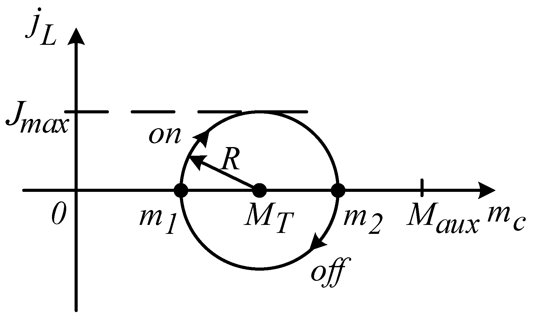
Since the charge pump circuit is considered lossless, the solution for the charge pump normalized voltage and the normalized inductor (winding) current traces a circuit in the normalized state plane as illustrated in
Figure 5. During the on-interval, the trajectory starts at
and moves clockwise towards
; whereas for the off-interval, it moves, still clockwise, from
, back to
. Here the initial charge pump normalized voltage is designated by
and
is its final normalized value.
Applying simple geometrical considerations to
Figure 5, one may conclude that in the periodic steady state the following condition must hold:
. Thus, equating (1) to (2) yields the auxiliary output voltage simply as
From (3) it is clear that the output voltage of the bias circuit, , tracks the main output voltage of the PFC, , while being offset by two diodes voltage drops. Since the main output is well stabilized the bias circuit output requires no additional regulation.
With the charge pump capacitor peak-to-peak voltage ripple is defined as the difference
, the average current,
, delivered to the auxiliary output can be derived from charge considerations
where,
is the switching frequency of the boost stage.
Using (3), the radii of the state-plane trajectory, see
Figure 5, can be found as
The current in the state plane is normalized relative to the base current
Realizing that
, see
Figure 5, and using (5) and (6) the peak current can be obtained:
where the resonant frequency is
.
From (7) the RMS current of each diode is found as
whereas the RMS current in the auxiliary winding is
3. Design Considerations
The required turns ratio can be obtained from (3) as
The equivalent leakage inductance can be estimated as about
of the boost inductance,
, and reflected to the auxiliary winding according to the turn ratio
The estimated value can be refined based on the measured parameters of the inductor at hand. Note that higher leakage helps to decrease peak currents and the associated conduction losses in the practical CICP circuit. Therefore, loose coupling between the main inductor and the auxiliary winding works better. In case the equivalent auxiliary winding inductance is still insufficient, a discrete component can be added at the auxiliary side.
The described above mode of CICP operation, see
Figure 5, prevails when the capacitor voltage,
, is within the range:
where the minimum charge pump voltage is:
and the maximum charge pump voltage is
Here (1) and (5) were used.
In DC/DC applications it is rather easy to fulfill (12), however, in PFC applications the output voltage of the line rectifier (i.e., the input voltage to the boost stage),
, periodically falls to zero. Here, (13) becomes negative so that condition (12) is violated when approaching the line voltage zero crossing. As a result of the CICP mode change, the output current of the charge pump falls short and a dip in the output voltage can be observed, see
Figure 3b.
To remedy the situation, first, the charge pump ripple should be limited. A “good” value of about
may be considered. From the considerations above and using (5), the design equation for the charge pump capacitor can be derived:
where,
is the maximum expected auxiliary output current.
A larger charge pump capacitor decreases the CICP resonant frequency and, according to (8), the RMS currents and associated conduction losses are also decreased.
Secondly, the output filter capacitor has to be chosen of a sufficient value to help ride through the zero-crossing dip. Also, to comply with the basic assumptions above, the value of the auxiliary output filter capacitor should be set substantially higher than the charge pump capacitor. Hence, the following simplified design criterion is suggested:
4. Verification
To prove the concept of the CICP, the circuit was first simulated in PSIM software. DCM boost PFC with the proposed CICP auxiliary bias circuit in
Figure 2 was designed for
RMS line to attain
and
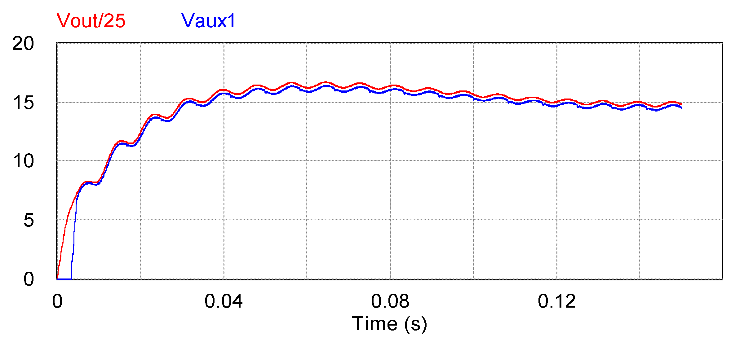
. Typical simulation waveforms (at circuit start-up) are shown in
Figure 6 (also see
Figure 3) and confirm the feasibility of the circuit. Note that since the auxiliary output follows the main output this also means that the percent ripple at the auxiliary output equals that at the main output.
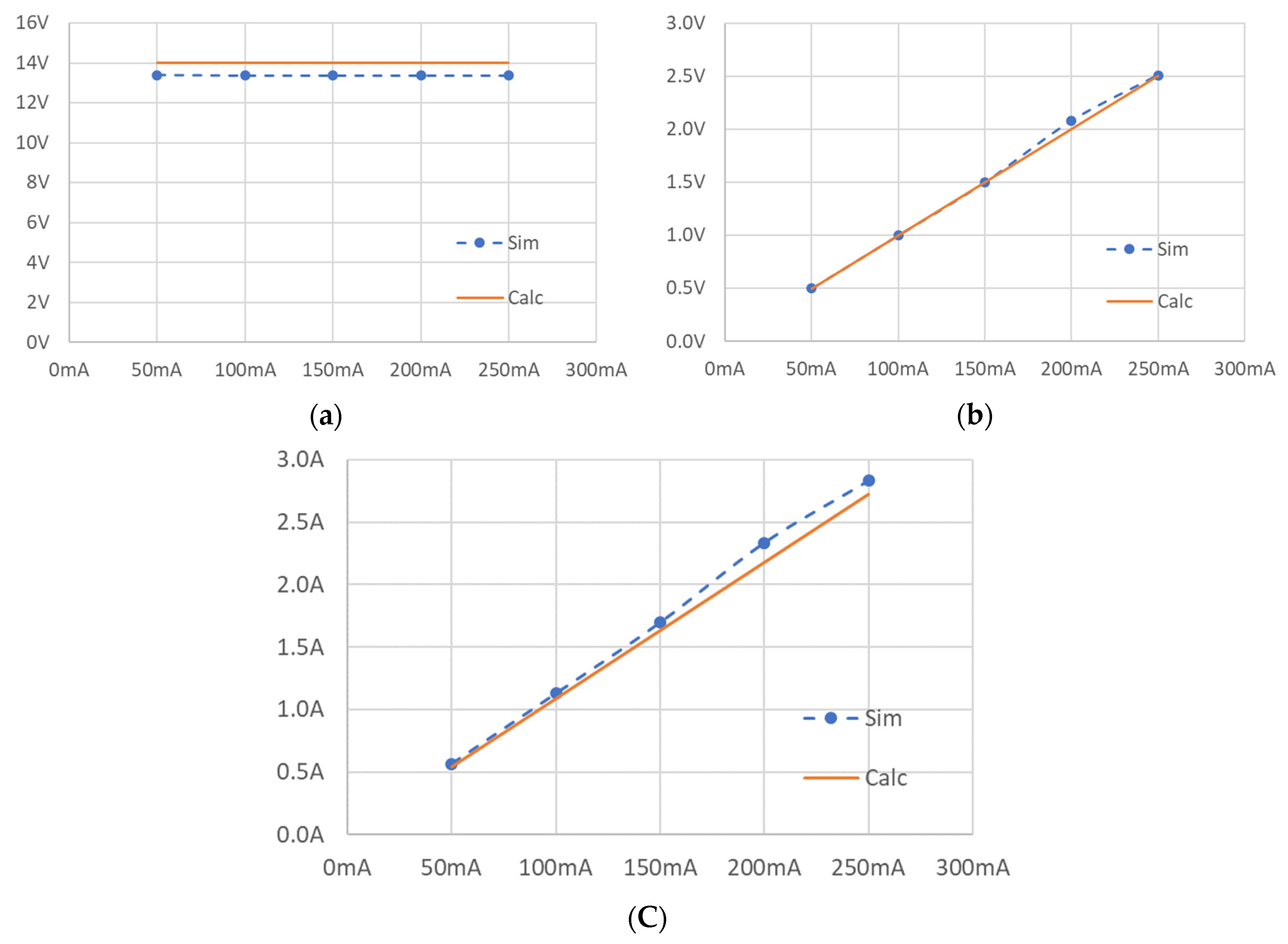
Figure 7a compares the calculated auxiliary output voltage (3) vs. the simulated values as a function of the DC current, I
aux, drawn from the auxiliary output. As predicted, the auxiliary voltage remains well stabilized.
Figure 7b compares the calculated vs. the simulated charge pump capacitor’s peak-to-peak ripple voltage (5) as a function of the auxiliary output current, I
aux.
Figure 7c shows the comparison of the calculated (9) vs. the simulated charge pump peak current as a function of the auxiliary output current, I
aux. Good agreement of the results was observed.
An experimental boost converter was also built and tested. The prototype was designed to operate in the discontinuous current mode and had the following parameters: input voltage
; main output voltage
; switching frequency
; boost inductor
. Single output isolated CICP in
Figure 2 was constructed with auxiliary to the main winding turns ratio
and the charge pump capacitors
. CICP was loaded with
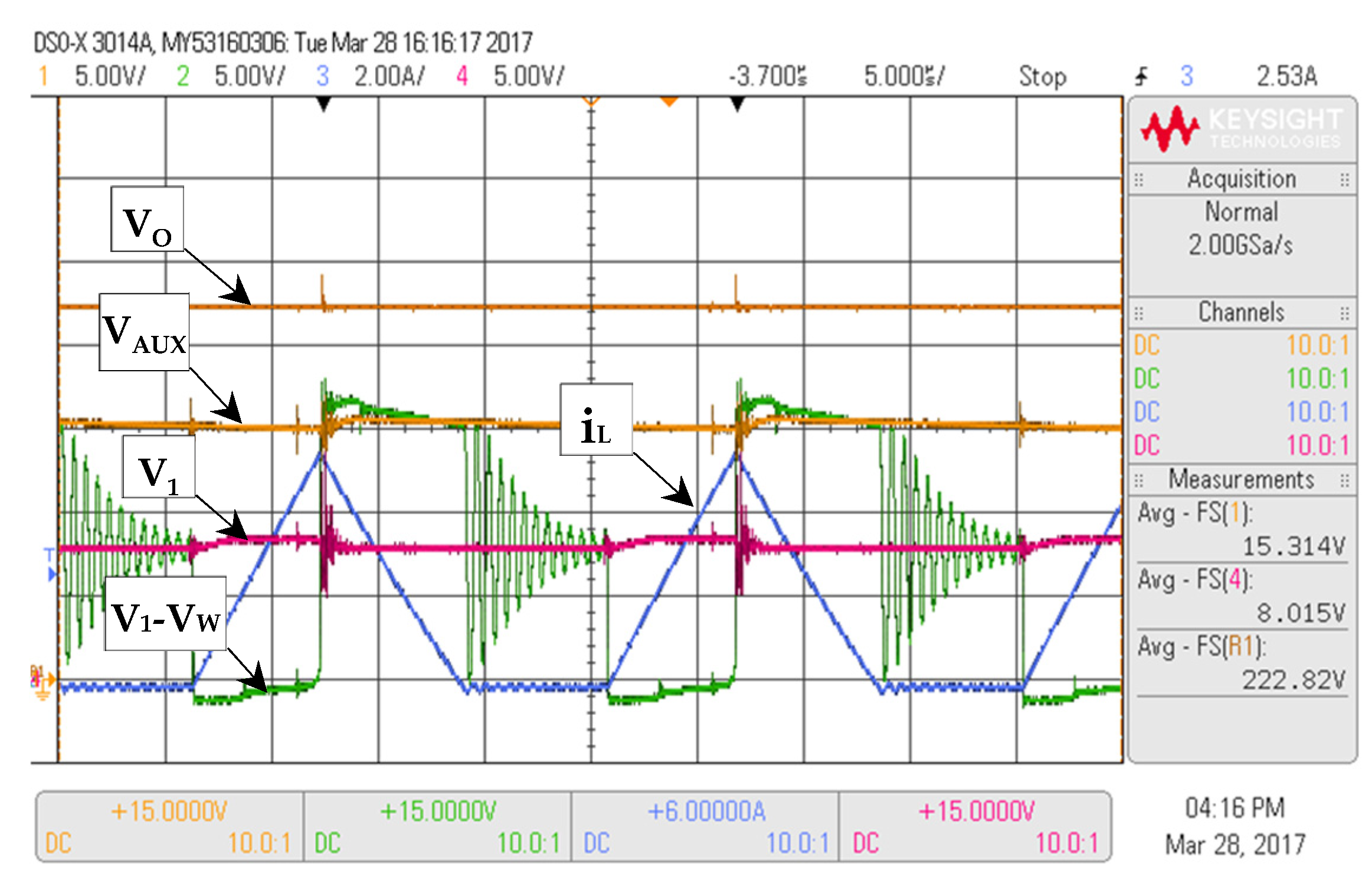
. Experimental waveforms are shown in
Figure 8. According to (3) the CICP bias circuit should provide
output. The measured auxiliary output voltage was
and matched the expected value. Accounting for the diode voltage drop, this result stands in good agreement with theoretical expectations.
Discussion
As shown above, the output voltage of the proposed bias circuit can track the main output voltage of the PFC rectifier regardless of the large swing of the rectified voltage, V
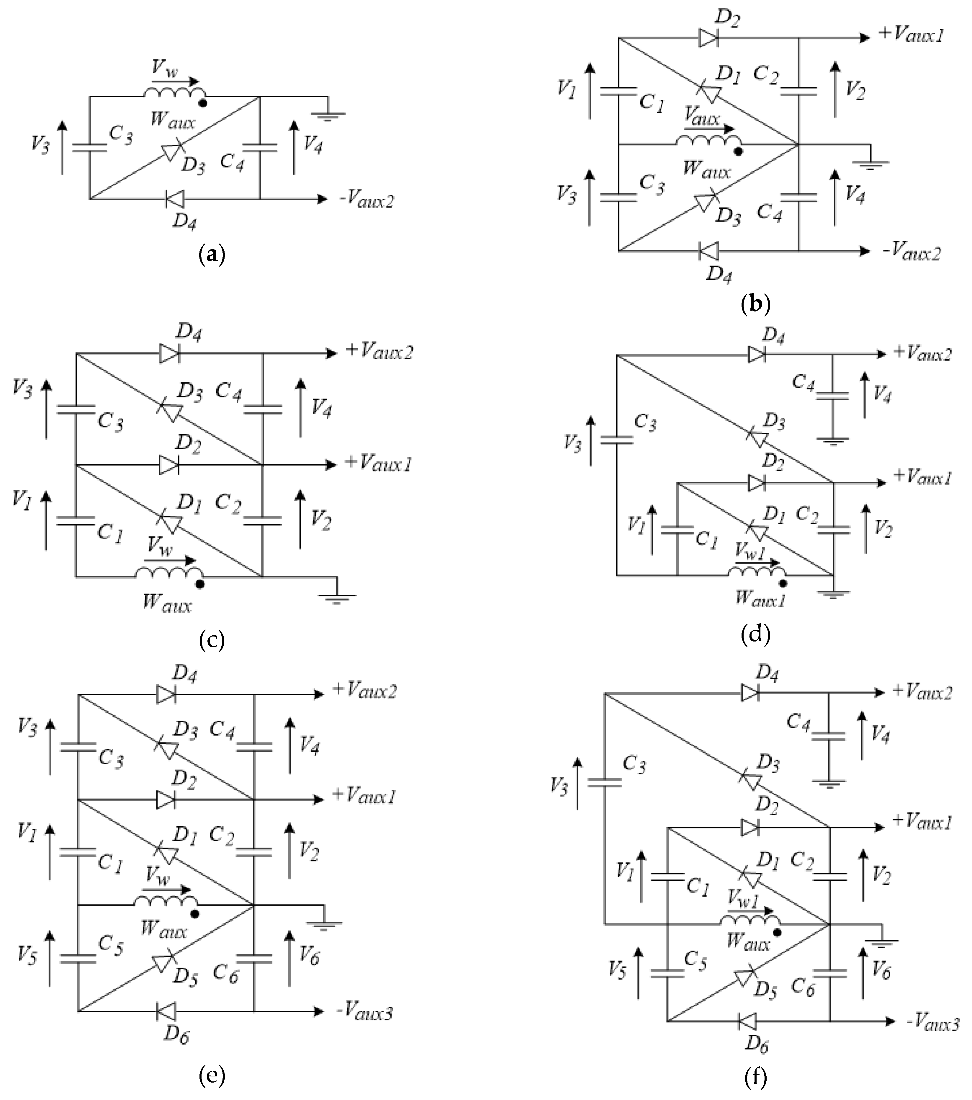
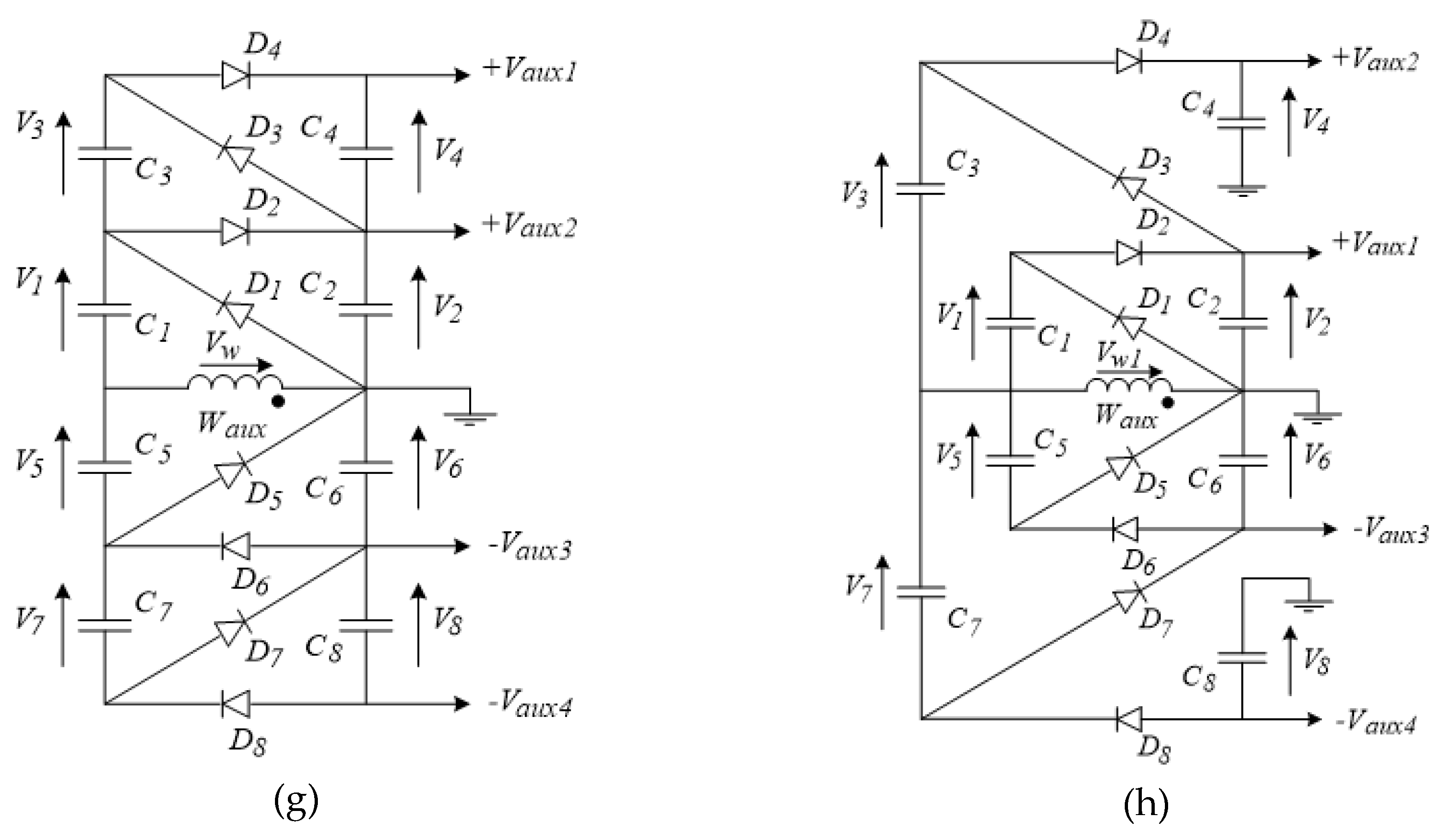
d, throughout the line cycle. Since the main output is well stabilized the bias circuit output requires no additional regulation. CICP can work with the power stage operating either in the continuous (CCM) or discontinuous (DCM) mode. The proposed principle is capable of extension, and several additional variants of the basic idea are illustrated in
Figure 9.
Single output negative bias supply can be derived either by simply interchanging the ground connection in
Figure 2 or using a complimentary CICP circuit shown in
Figure 9a. Yet again, a stabilized negative voltage, -V
aux2, is attained at the output of the bias circuit.
Either positive or negative dual voltages can be derived from
Figure 9b by interchanging the ground and one of the auxiliary outputs. Another option is using a two-stage Greinacher (aka Cockcroft–Walton) multiplier as shown in
Figure 9c. Yet another option is applying the modified Dickson charge pump as shown in
Figure 9d. Both circuits can provide bias voltages with approximately 1:2 ratio, however, the Dickson charge pump has the advantage of higher capacitance to ground for the V
aux2 output and, considering the capacitors’ ESR, also provides lower impedance to ground.
CICP bias circuit can be further extended by adding more stages any multiples of the nV
out voltage (either positive or negative or both) may be obtained as shown in
Figure 9e–h.
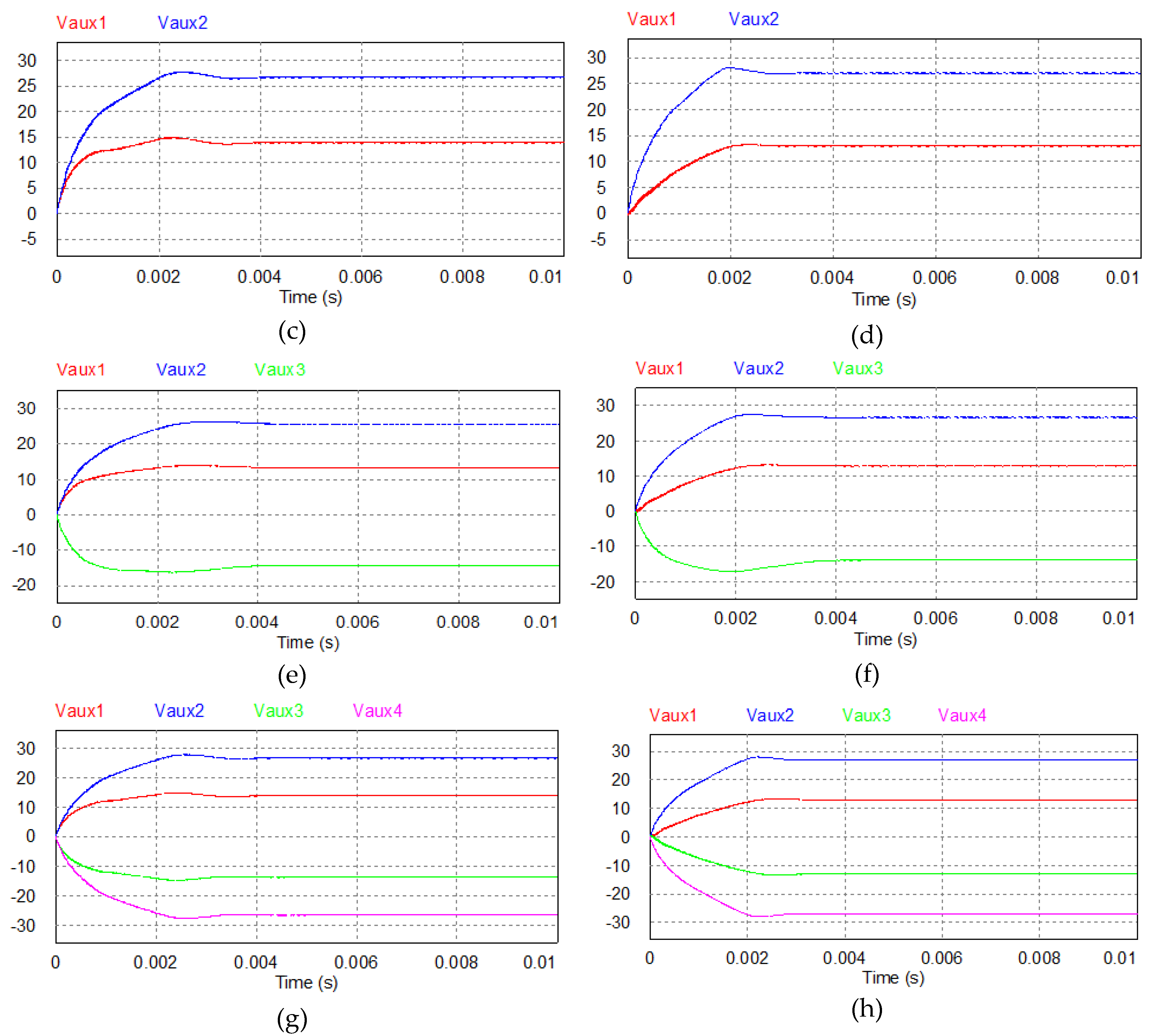
The proposed family of bias circuits was verified by cycle-by-cycle simulation. Simulated waveforms of CICP bias circuits in
Figure 9 are shown in
Figure 10. The operation of the CICP family matched the theoretical expectations.
In practice, however, as the number of stages is increased, the voltages of the higher stages begin to “sag”, primarily due to the diode voltage drop. Therefore, low-voltage Schottky diodes should be used for their fast switching speed and low-voltage drop.
Multiple arbitrary output voltages can be attained by combining the proposed CICP approach with off-the-shelf charge pump ICs, which can offer fixed or adjustable output voltage and greater design flexibility while saving footprint area, weight, and cost of the bias circuit [
18].
Conclusions
This brief is concerned with a passive, low-cost, self-bias auxiliary bias circuit for boost-derived converters based on a charge pump circuit. The bias circuit inherently follows the main regulated output and, therefore, can provide a well-regulated voltage suitable to power the control circuits.
Analysis, analytical solutions, and design guidelines were presented. Theoretical predictions were first verified by simulation. Then, the proposed bias circuit prototype was tested with the prototype boost PFC rectifier stage in either continuous or discontinuous conduction mode. The output current of an excess of was attained.
The advantage of the proposed bias circuit in
Figure 2 over the earlier counterpart in
Figure 1 is that it lends itself to extension. As shown in the paper, a family of self-bias circuits with multiple outputs was developed. The proposed bias circuits are isolated from the main power stage and completely passive. All of the outputs were shown to inherently follow the main regulated output of the boost converter and thus provide a stable output voltage.
The concept of the offered bias circuits can also be easily extended to other converter topologies such as Cuk and SEPIC derived.
The advantages of the proposed bias solutions are simple design, multiple outputs, reduced hardware and footprint, and low cost.
Figure 1.
Earlier art: doubler rectifier auxiliary bias circuit for boost PFC rectifier [
5].
Figure 1.
Earlier art: doubler rectifier auxiliary bias circuit for boost PFC rectifier [
5].
Figure 2.
Proposed Boost PFC rectifier with the CICP auxiliary self-bias circuit.
Figure 2.
Proposed Boost PFC rectifier with the CICP auxiliary self-bias circuit.
Figure 3.
Typical time domain waveforms of the CICP: on the switching period scale featuring: upper trace - power switch gating voltage, , middle trace- auxiliary winding current, , bottom trace- charge pump capacitor voltage, (a); on the line frequency scale in PFC applications featuring: upper trace – the rectified line voltage, , and the output voltage, ; middle trace- charge pump voltage, , bottom trace- auxiliary output voltage, (b).
Figure 4.
Equivalent circuits of the CICP during main switch on time - the charge pump charging (a); main switch off time - the charge pump discharging to the auxiliary output (b).
Figure 4.
Equivalent circuits of the CICP during main switch on time - the charge pump charging (a); main switch off time - the charge pump discharging to the auxiliary output (b).
Figure 5.
CICP solution trajectory in the normalized state plane.
Figure 5.
CICP solution trajectory in the normalized state plane.
Figure 6.
Simulated waveforms of the CICP auxiliary bias circuit driven by a boost PFC. The auxiliary output follows the regulated main output.
Figure 6.
Simulated waveforms of the CICP auxiliary bias circuit driven by a boost PFC. The auxiliary output follows the regulated main output.
Figure 7.
Comparison of the calculated vs. the simulated values as a function of the auxiliary output current: (a); (b); (c).
Figure 7.
Comparison of the calculated vs. the simulated values as a function of the auxiliary output current: (a); (b); (c).
Figure 8.
Experimental waveforms of basic CICP. Top to bottom: the output voltage , the auxiliary output voltage , charge pump voltage , the rectified voltage , inductor current .
Figure 8.
Experimental waveforms of basic CICP. Top to bottom: the output voltage , the auxiliary output voltage , charge pump voltage , the rectified voltage , inductor current .
Figure 9.
Variants of the CICP bias circuit: (a) Complementary with negative output; (b) Dual bipolar; (c) Dual unipolar (w/ Greinacher multiplier); (d) Dual unipolar (w/Dickson pump); (e) Triple bipolar (w/ Greinacher multiplier); (f) Triple bipolar (w/Dickson pump); (g) Quadruple (w/ Greinacher multiplier); (h) Quadruple (w/Dickson pump).
Figure 5.
Simulated output voltages of the CICP bias circuits: (a) Complementary with negative output; (b) Dual bipolar; (c) Dual unipolar (w/ Greinacher multiplier); (d) Dual unipolar (w/Dickson pump); (e) Triple bipolar (w/ Greinacher multiplier); (f) Triple bipolar (w/Dickson pump); (g) Quadruple (w/ Greinacher multiplier); (h) Quadruple (w/Dickson pump).
