1. Introduction
Terahertz (THz) waves represent a segment of the electromagnetic (EM) spectrum falling between microwaves and infrared radiation, spanning the frequency range of 0.1 THz to 10 THz. These frequencies have garnered significant attention as potential carrier waves for the upcoming Beyond 5G or 6G cellular networks due to their ultra-large bandwidth, which is deemed essential for advancing wireless communication [
1,
2,
3,
4,
5,
6]. The exploration of THz radiation sources has primarily focused on electronics and photonics-based devices. Notable examples of electronics-based sources include advanced CMOS-based sources [
7,
8,
9], heterojunction bipolar transistors (HBTs) [
10,
11,
12], high electron mobility transistors (HEMTs) [
13,
14,
15], resonant tunneling diodes (RTDs) [
16,
17], and Schottky barrier diodes (SBD) [
18,
19,
20,
21]. While these all-electronic sources offer advantages in terms of flexibility, integration, and cost-effectiveness, they face challenges related to delivering higher power at higher frequencies [
22]. Radio frequency (RF) amplifiers, though capable of partially compensating for power limitations, introduce drawbacks such as high noise figures and restricted amplifier bandwidth. In addition to electronics-based sources, photonics-based devices utilizing the photomixing technique with a uni-travelling carrier photodiode (UTC-PD) have been extensively investigated. These devices leverage photonics technologies, providing advantages such as tunability, broad operating bandwidth, and the ability to transmit and manipulate THz signals with minimal loss across a wide frequency range [
23,
24,
25]. However, UTC-PD-based photomixers suffer from insufficient output power for practical transmission distances. One contributing factor to the output saturation of UTC-PDs is the space-charge effect in the carrier transport region, exacerbated by the need to increase bias voltage, leading to heat generation [
26,
27,
28]. Consequently, there is a pressing need to develop device structures that reduce space charge and improve heat dissipation.
Various strategies have been proposed to address the power limitations associated with a single UTC-PD. These include PD epitaxial layer modification and optimization [
28,
29], monolithic integration of impedance matching circuits with UTC-PDs [
30,
31], and power combining. Power combining, in particular, has been implemented by techniques such as spatial power combining using planar antenna arrays [
32,
33], multilayer packaging technology integrating arrayed UTC-PDs with a rectangular waveguide (WR) power combiner [
34], and the use of planar transmission line power combiners [
35]. Additionally, the adoption of high thermal conductivity materials is considered a viable solution to mitigate thermal issues, given that the poor thermal conductivity of Indium Phosphide (InP) poses a significant hindrance to achieving higher output power from a single UTC-PD.
In this article, we present a demonstration of the power combining approach using a 2 by 1 microstrip line-based Wilkinson combiner integrated with a rectangular patch antenna at 300 GHz. The use of microstrip line (MSL) transmission technology is a suitable method for efficiently combining large-scale currents because its cascading geometry is simpler compared to other transmission line types such as a strip line and a coplanar waveguide (CPW). The objective is to combine photocurrents from two parallel connected UTC-PDs, thereby addressing the power limitations inherent in conventional single UTC-PDs. Furthermore, the chip was fabricated on silicon carbide (SiC), chosen for its superior thermal conductivity compared to InP. Heat dissipation capability is a crucial consideration in the context of RF output power from UTC-PDs, and the use of heterogeneous substrates with higher thermal conductivity, such as SiC, that has a seven times higher thermal conductivity than InP, offers a promising solution to this challenge.
2. A Uni-travelling Carrier Photodiode (UTC-PD)
In 1997, NTT Laboratories presented an innovative advancement in photodiode technology with the introduction of a uni-travelling-carrier photodiode (UTC-PD), that exhibited a superior operational speed and higher saturation current (wider output linearity), compared to the conventional PIN photodiode [
25]. The distinctive structure of the original UTC-PD featured a relatively thin p-type absorption layer, where minority carrier electrons were generated, diffused, and accelerated towards the collection layer. Within the depleted collection layer, electrons exhibited a near-ballistic velocity, effectively minimizing the contribution of slow hole transport to the photodiode response. Since its invention, several UTC-PD modifications have been proposed to enhance their performance by adjusting layer structures. To reduce electron traveling time within the absorption layer, the incorporation of a quasi-field through band-gap grading and/or doping grading has proven effective [
27,
28]. Additionally, strategies such as cliff-like structures have been employed to optimize the electric field profile and improve electron velocity saturation within the collection layer [
29]. Also, moderate n-type doping in the collection layer has been identified as preferable for increasing the saturation current [
27]. Furthermore, the combination of neutral and depleted absorption layers has been shown to enhance responsivity without significantly compromising saturation current or operational speed. Another approach to augment responsivity while preserving operational speed involves the utilization of external structures to guide input light to the absorption layer at varying angles, including waveguide structures, refracting facets, or total reflection structures, and evanescent coupling [
36].
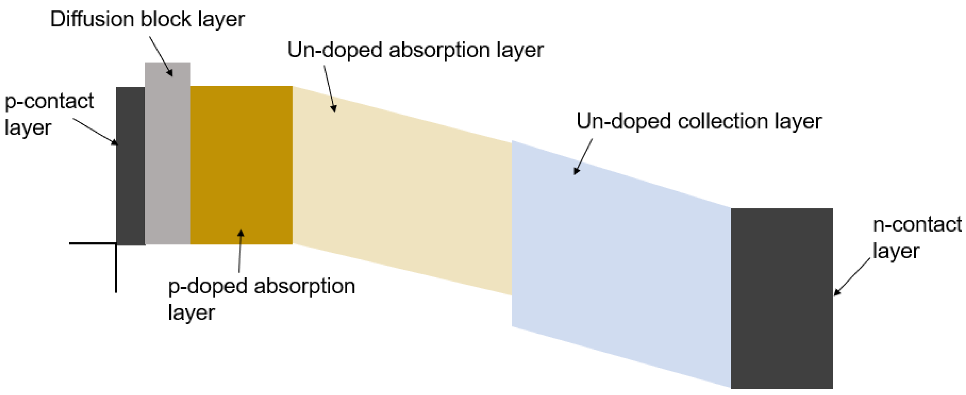
Figure 1 illustrates a representative layer structure of the modified UTC-PD, strategically balancing the trade-off between bandwidth and responsivity through the composite use of UTC and PIN structures. This structure remains adaptable, with possibilities for further enhancements. In practical applications, UTC-PDs are normally integrated with either planar antennas such as bow-tie, slot, and patch antennas, or rectangular waveguides (WRs) integrated with planar CPW to WR transition lines. The continuous evolution of UTC-PD technology underscores its significance in the realm of photodetectors, offering a versatile platform for innovation and improvement, and the pursuit of optimized UTC-PD designs and functionalities continues to be a focal point in contemporary research, with potential implications for the ongoing development of advanced photonic devices.
3. Continuous THz Wave Generation by Photomixing with a UTC-PD
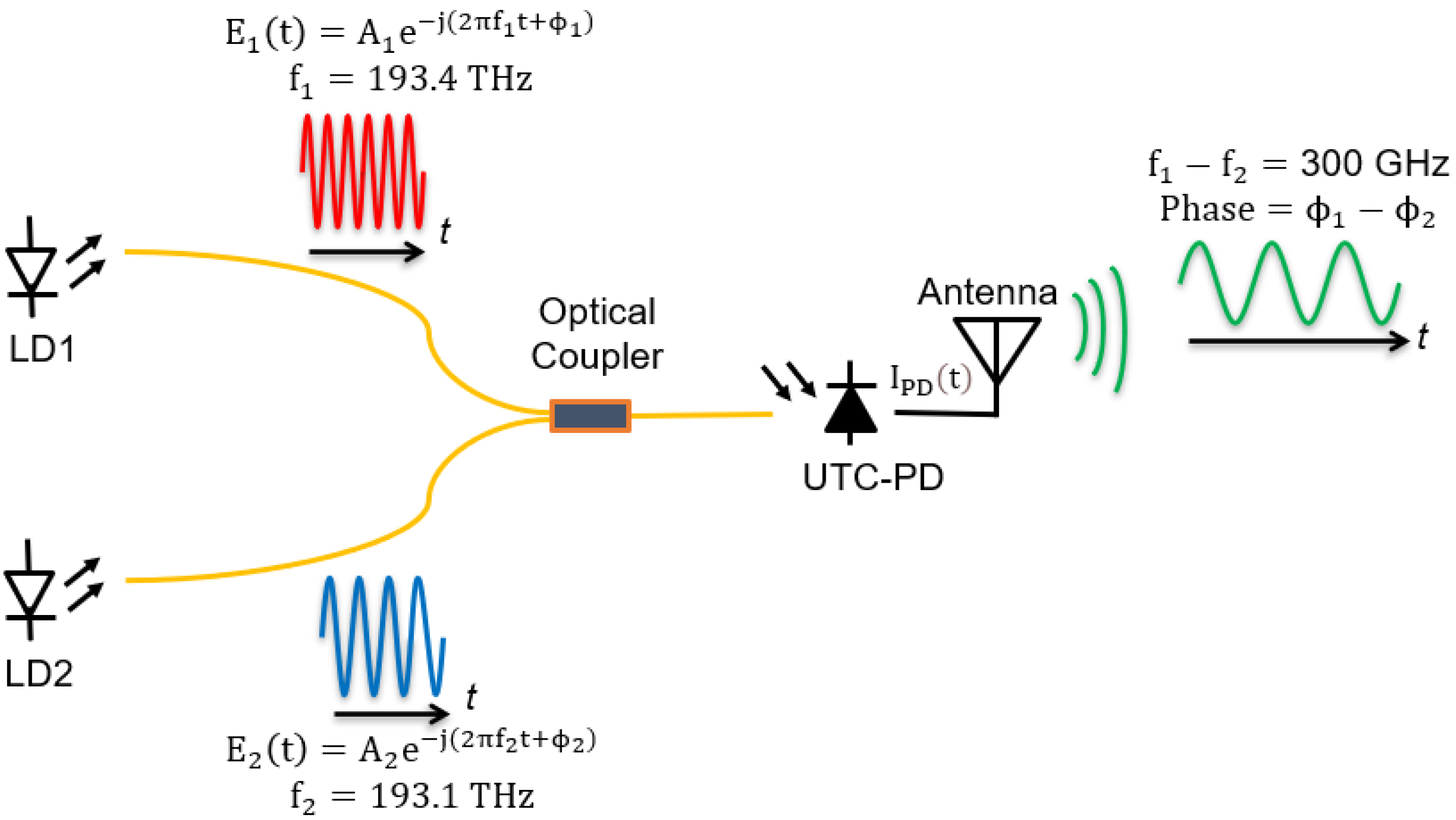
Figure 2 depicts the photomixing concept (optical heterodyning) at the UTC-PD to generate a continuous THz wave.
In a photomixing system, two spatially overlapped laser beams characterized by frequencies (f
1 and f
2) and phases (ϕ
1 and ϕ
2), and having identical polarization, are combined, and converted into an alternating current at the ultra-fast InGaAs UTC-PD with a frequency equivalent to the frequency difference between the two lightwaves. The electric fields of the two lightwaves (optical beats) can be expressed as
where
and
are the electric field amplitudes of the two lightwaves. When the optical beats are coupled to the UTC-PD, the generated photocurrent
is
where R is the responsivity UTC-PD that corresponds to the current generated per watt of incident optical power, and N(t) represents the noise effects during optical-to-THz conversion [
37]. The photomixing technique provides a notable advantage of allowing for precise tuning of the output frequency. This is achieved through the exploitation of the difference in frequency between the two lasers involved in the process. [
38].
4. Device Design and Fabrication
Initially, the UTC-PD epilayers were grown on a semi-insulating (S.I.) InP substrate by metal organic chemical vapor deposition (MOCVD) at low-pressure. The absorption layer comprises of p-InGaAs, thin p+InGaAs, and thin undoped InGaAs, while the collection layer consists of thin undoped InGaAsP, thin undoped InP, thin n+InP, and lightly n-doped InP. The absorption layer has a total thickness of 0.13-µm and an area of 12.5 µm
2 (4-µm diameter) while the collection layer thickness is 0.23-µm. The p-InGaAs absorption layer was moderately doped to leverage the advantages of the self-induced field (self-bias effect) within the absorption layer [
39]. To mitigate current blocking at the interface of the absorption and collection layers, a step-graded band-gap profile was employed, incorporating an InGaAsP layer with a typical band-gap energy of approximately 1 eV between the InGaAs absorption and InP collection layers.
Next, the UTC-PD epitaxial wafer, which had an InP substrate, was affixed onto a glass supporting substrate. The InP substrate was completely removed by mechanochemical polishing as well as selective chemical etching at the InP/InGaAs interface. Following this, a 10 nm amorphous Si layer was deposited onto the surface. This substrate was then wafer-bonded to a SiC substrate that was thinned to 32-µm. The entire process was conducted at room temperature, with a high pressure of approximately 20 MPa to prevent any potential deterioration of the device characteristics [
40]. Ultimately, the glass supporting substrate was detached from the epi-layers, leaving only the UTC-PD epi-layers on the SiC substrate, maintaining the same layer order as they were grown on the InP substrate. The UTC-PDs were fabricated with the microstrip line-based Wilkinson combiner, featuring 50 Ω input lines and a patch antenna on the SiC substrate.
The optimized integrated design details of the 2 × 1 Wilkinson power combiner and the rectangular microstrip patch antenna using a 3-D full-wave electromagnetic simulator before UTC-PD integration can be referred to in our previous work reported in [
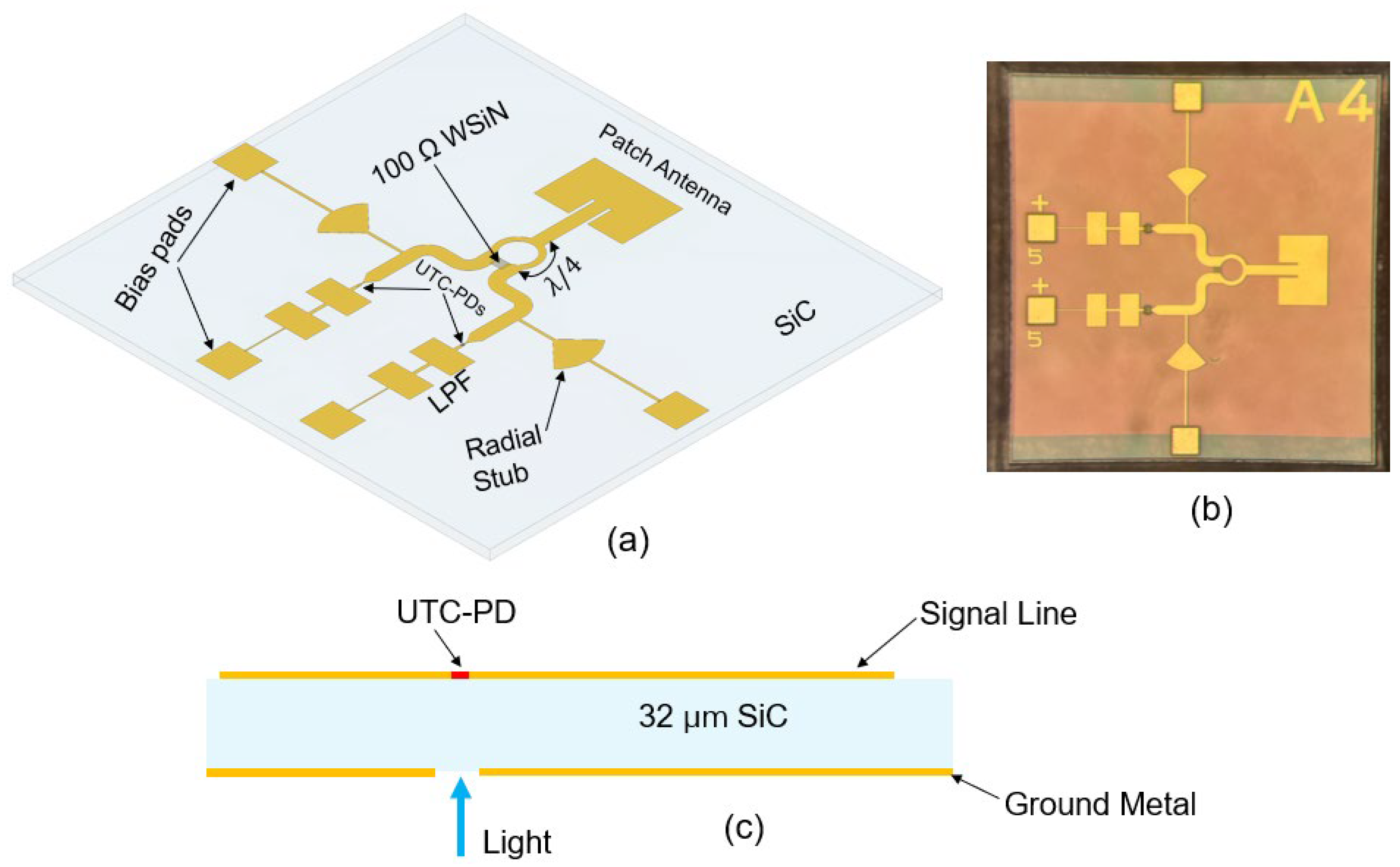
41]. The rectangular microstrip patch antenna is used because of its low profile thereby easing the fabrication process. It is important to highlight that although antenna integrated devices have a lower maximum output power compared to waveguide-output devices, they demonstrate greater suitability as frequencies increase. This is attributed to their ability to operate without the need for precise metal cutting in small aperture waveguides and their flexibility to create either a broadband or resonant-type module by choosing the type of the integrated antenna. The designed monolithic integrated device is illustrated in
Figure 3.
On the 32 µm thick SiC substrate with a dielectric constant εr = 10, the Wilkinson power combiner was designed consisting of two 50-Ω characteristic-impedance input microstrip lines with a width of 30.6 µm and 250 µm apart corresponding to the fiber array pitch, and two 70.71 Ω quarter wavelength transformer lines with a width of 13.3 µm. It’s worth noting that because of the resistor between the two input ports, a Wilkinson power combiner offers relatively higher isolation and better matching between the two ports compared to other combiners such as a T-junction combiner. A Tungsten Silicon Nitride (WSiN) layer is used to achieve the 100 Ω isolation resistance that corresponds to 2Z0 where Z0 is the characteristic impedance of the input lines. The resistor does not dissipate power thus rendering the Wilkinson power combiner to be theoretically lossless. However, in practice, there may be some losses, although they are typically minimal. A microstrip patch antenna is known to have a high impedance at its edges and low impedance in its center. The impedance at the edge of the designed patch antenna is 495 Ω and is matched to the 50 Ω line by the inset feed technique with an inset length of 59 µm and a width of 46 µm.
A five-section stepped-impedance
low pass filter (LPF) with 110 Ω and 25 Ω as the highest and lowest impedance respectively, as well as a radial stub with high impedance lines of 92 Ω were used as RF chokes in the UTC-PD biasing circuits to avoid RF signal leakage into the DC bias line. The simulated frequency response of the choke filters, shown in
Figure 4, demonstrated that the stepped-impedance LPF achieves an attenuation of over 10 dB, while the radial stub choke provides approximately 7.5 dB attenuation at 300 GHz. Moreover, the radial stub also helps to compensate for the UTC-PD junction capacitance.
5. Device Characterization
In this section we give a detailed account of the experimental setup and measurements taken to characterize the device that include the combining coherency of the UTC-PD photocurrents by the Wilkinson combiner as well as the device output linearity.
5.1. Experimental Setup
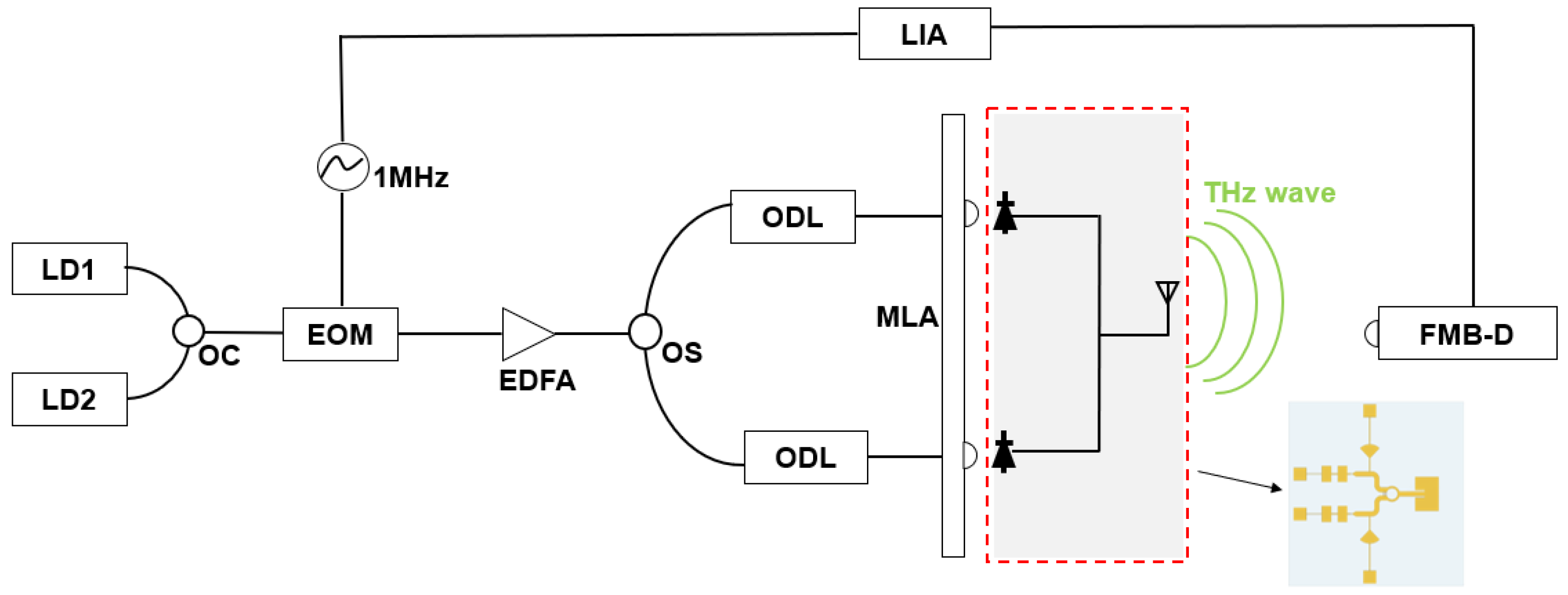
The experimental setup for device characterization is shown in
Figure 5.
Two wavelength tunable laser diodes, LD1 and LD2 emitted lightwaves in the 1550 nm band (193.1 THz and 193.4 THz, respectively) with a power of 10 dBm. They were coupled to generate an optical beat signal with a frequency difference of 300 GHz using an optical coupler (OC). The optical beat signal was then intensity modulated at 1 MHz by an electro-optic modulator (EOM). It was then amplified using an Erbium doped fiber amplifier (EDFA) and split into two optical paths by an optical splitter (OS). To ensure phase synchronization of the split signal, the length of the two paths were adjusted using optical delay lines (ODLs). Subsequently, the two lightwaves were directed onto a micro lens array (MLA) and coupled to the two UTC-PDs which were integrated with a Wilkinson power combiner and a patch antenna. The 300 GHz wave was radiated vertically and detected using the Fermi-level managed barrier diode (FMB-D) [
42], [
43], [
44] with two THz lenses with 25 mm aperture. It is affixed to a mechanically controlled rotation stage at 32 mm away from the device. The rotation angle is defined as that from the vertical direction to the device. The relative intensity was measured using a lock-in amplifier (LIA).
5.2. Combined Photocurrent Coherency
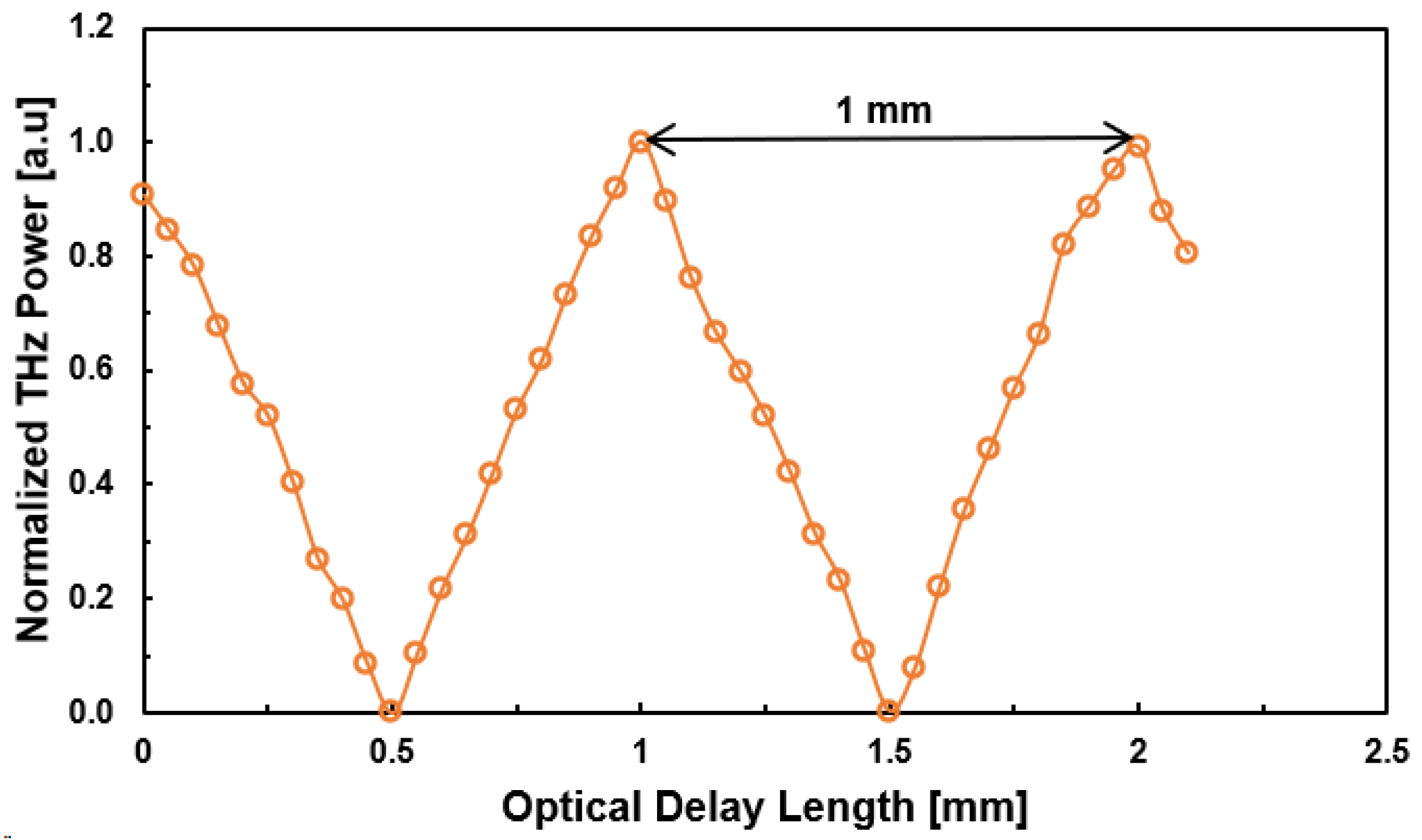
We examined the coherent combining of photocurrents from the two UTC-PDs by the Wilkinson power combiner. To ensure coherent signal combining in a 2 by 1 Wilkinson power combiner, it is imperative for the phases of the two alternating currents generated at the UTC-PDs that are fed to the combiner to be identical. This entails aligning the peaks and troughs of the two currents, resulting in constructive interference and optimal signal combining efficiency. To manipulate the phases of the two lightwaves traveling through different optical paths, we employed a manually operated optical delay line (ODL). By adjusting the length of the optical path, we were able to vary the phase of the alternating currents generated at the UTC-PDs. This enabled us to control the observed interference pattern when the two alternating currents were combined. In
Figure 6, we plotted the power of the 300-GHz wave detected by the FMBD. The resulting graph showed a clear interference pattern with a period of 1 mm, which corresponds to the expected interference period between two 300-GHz alternating currents. Additionally, the fact that the power decreases to zero confirms that the Wilkinson combiner enables an ideal coherent combining of the two 300 GHz alternating currents generated at the UTC-PDs.
5.3. Output Linearity and Satuartion due to Space Charge Effect
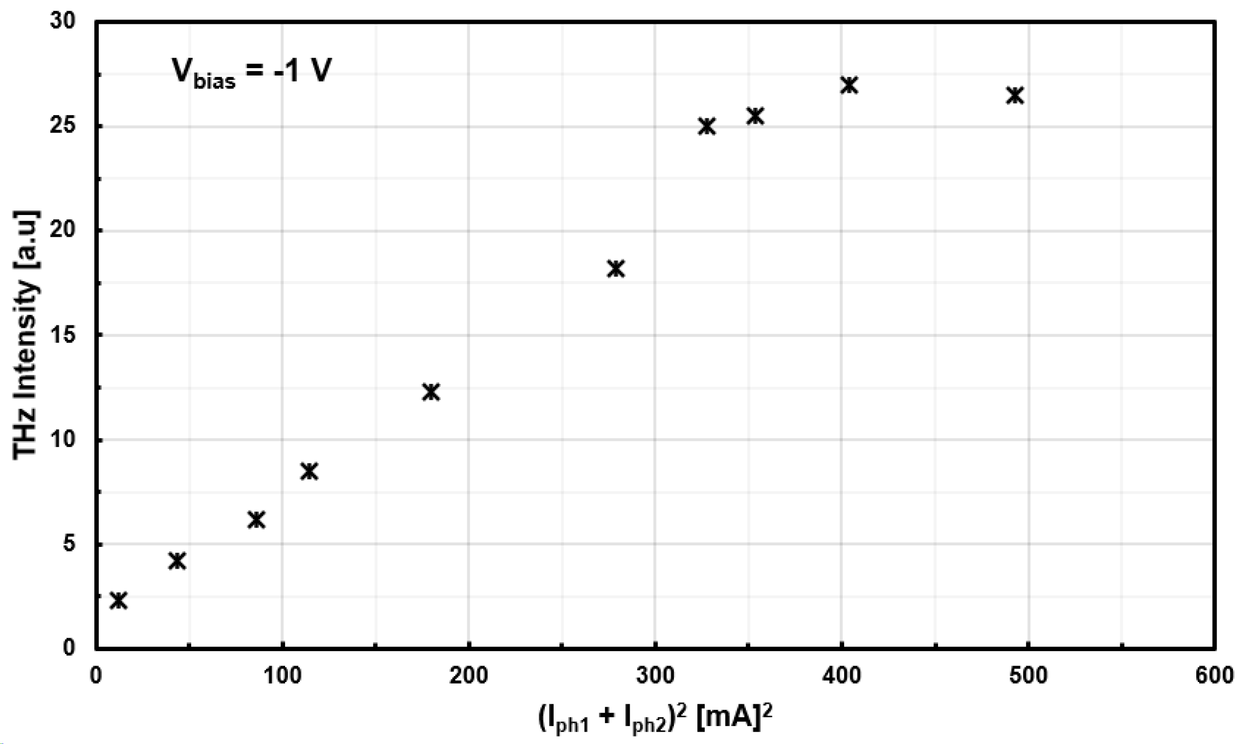
We measured the output linearity at 300 GHz by assessing the output power with respect to the total photocurrent generated by the two UTC-PDs (I
ph1 + I
ph2) at a DC bias voltage of -1 V. Prior to the measurement, the ODL was meticulously tuned to ensure that the device would generate the maximum output power. To prevent performance degradation or damage to the device, measurements were conducted up to 21 dBm input optical power that yielded photocurrents of 11.3 mA and 10.9 mA from UTC-PD1 and UTC-PD2, respectively. As illustrated in
Figure 7, up to around 10.2 mA and 9.9 mA from the two photodiodes respectively, the results are almost in agreement with the theoretical definition that the radiated power is proportional to the square of the photocurrent when we assume that the AC current is proportional to the DC current. The slight discrepancy potentially arises due to bias dependency in UTC-PDs, causing variations in the actual bias across the PDs at a fixed external bias voltage as photocurrent changes. It is needful to note that difference between the photocurrents from the two UTC-PDs at the same optical power is less than 3%. It could potentially be attributed to the slight misalignments between the two UTC-PDs and the micro lens array, resulting in slight disparities in the intensity of the lightwave irradiated on each UTC-PD.
The output saturation beyond 20 mA total photocurrent from the two UTC-PDs is induced by carrier space charge effect. This can be described in regard to the critical current density
Jmax for a given voltage (-1 V) that modulates the field profile therein causing a non-linear response and output saturation. Nonetheless, it is important to note that due to electron velocity overshoot phenomenon, the field modulation by space charge effect is considerably less in a UTC-PD. Consequently, a UTC-PD is capable of delivering a substantially greater output saturation level in comparison to a conventional pin-PD. The electron velocity in the InP UTC-PD collection layer has been reported to be between 4 × 10
7 cm/s - 6 × 10
7 cm/s [
28]. Since the absorption area of the UTC-PD used is 12.5 µm
2, the measured peak photocurrent of 10 mA indicates that the critical current density is 80 kA/cm
2. This is in agreement with the theoretical
Jmax estimated to be between 64 – 96 kA/cm
2 using
where the electron charge
, the carrier density
, and the electron velocity
[
28].
6. Current Combining for Enhanced Radiated THz Power
The UTC-PD is a current source that produces a photocurrent (
) proportional to the intensity of the incident lightwave and given as
where
is the direct current component,
is the alternating current (AC) component that contributes to the THz emission and is given as
where
is the amplitude of the alternating current,
and
are the frequency and the initial phase, respectively [
45,
46].
If the lightwaves incident on the two UTC-PDs are of the same phase, the Wilkinson combiner will coherently add the photocurrents from the two UTC-PDs with amplitudes
and
. The radiated power from the antenna will then be
where
is the radiation resistance of the antenna.
Based on the analysis above, it can be inferred that when
N lightwaves with identical phases are coupled to
N combined UTC-PDs, the resulting output current ideally multiplies by a factor of
N, and the radiated wave intensity from the antenna amplifies by
N2. In our specific scenario, we employed a 2 by 1 Wilkinson power combiner [
40] to combine the currents from two UTC-PDs. This implies that the resultant power radiated from the antenna connected to the combiner would theoretically be 6 dB higher when two UTC-PDs are irradiated relative to one UTC-PD irradiation.
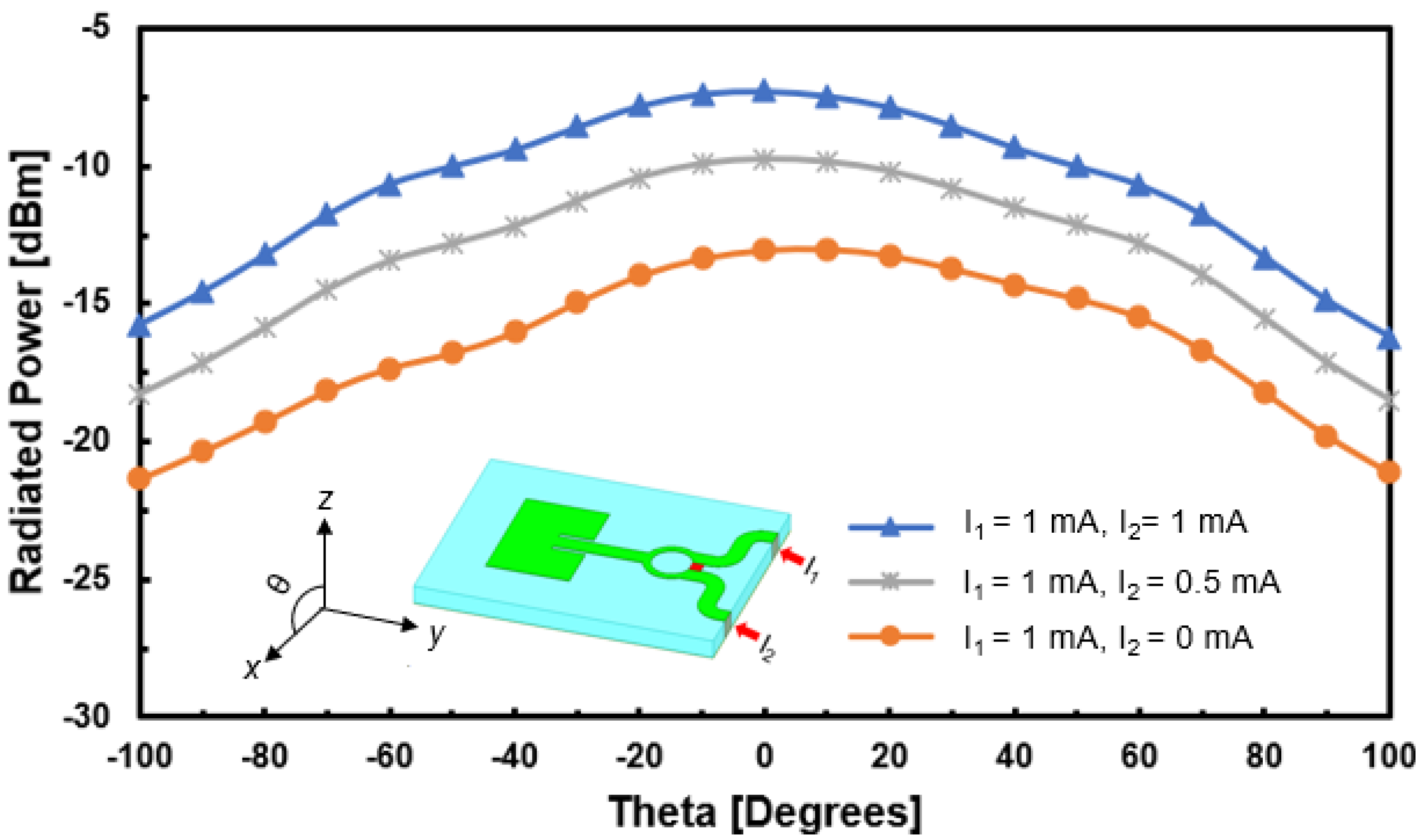
Figure 8 shows the simulation results of the radiated power for the 2×1 integrated Wilkinson combiner-antenna device as a function of the angle theta (θ) using a 3-D full-wave electromagnetic simulator (Ansys HFSS) with the two signal sources modelled as current sources alluding to a UTC-PD. When I
1 = 1 mA, I
2 = 0 mA, the maximum radiated power is -13 dBm in the upward direction, whereas it is -9.7 dBm for I
1 = 1 mA, I
2 = 0 mA and -7.3 dBm for I
1 = 1 mA, I
2 = 0 mA, which indicates a 3.3 dB and a 5.7 dB increase in radiated power, respectively.
We verified the above theoretical assertion with the experimental setup depicted in
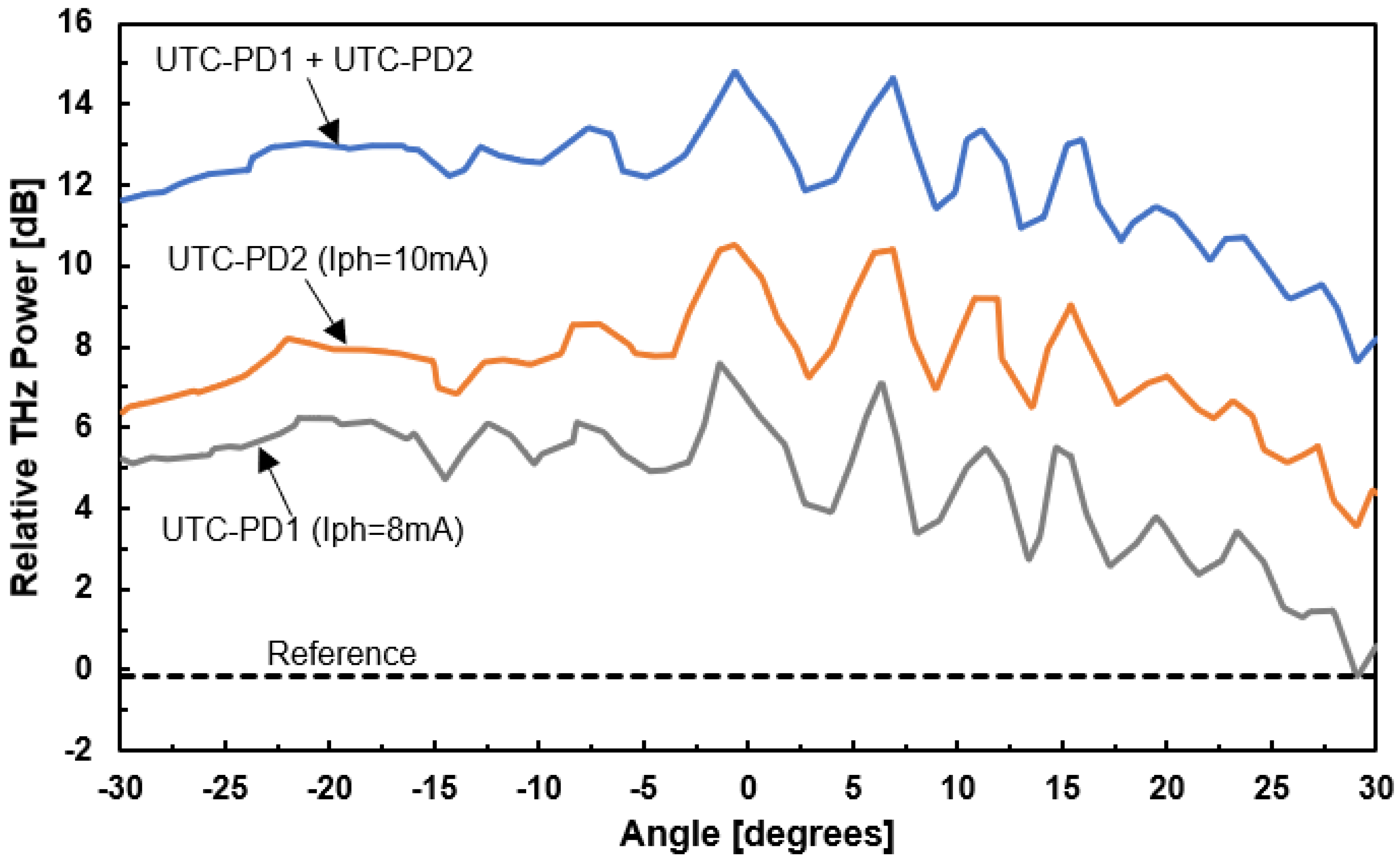
Figure 5. For relative radiated power measurement, the minimum detected power at a beamwidth of 60 degrees from the vertical axis when activating one UTC-PD was defined as a reference (0 dB).
Figure 9 illustrates that at around -1 degree, the measured relative peak power was 7.5 dB when UTC-PD1 with a photocurrent of 8 mA was activated and 10.4 dB for UTC-PD2 with a photocurrent of 10 mA. Then, when we activated both UTC-PDs (18 mA), the relative peak power reached 14.8 dB, indicating a 7.3 dB increase in power relative to the power obtained with UTC-PD1 (8 mA) and a 4.4 dB increase in power relative to the power obtained with UTC-PD2 (10 mA). This implies that when the photocurrent was multiplied by 2.25 times, the radiated power increased by 5 times and when the photocurrent was multiplied by 1.8 times, the radiated power increased by 2.75 times. Although there are some losses, these results are largely in agreement with the theory that when the photocurrents are multiplied by a factor of N, the radiated power will increase by a factor of N
2.
7. Conclusions
A thorough analysis and characterization of a novel device monolithically integrating two UTC-PDs connected in parallel, a microstrip line-based Wilkinson power combiner and a rectangular patch antenna on a SiC substrate for enhancement of THz wave power is presented. We have given a thorough theoretical analysis and an experimental demonstration that if the phases of the photocurrents fed to the combiner are the same, they will be coherently combined by the Wilkinson combiner and that if the photocurrent being fed to the antenna is multiplied by a factor of N, the radiated power will be enhanced by N2. We have further demonstrated that the UTC-PD output saturation depends on space charge effect that is brought about by a critical charge density that is about 80 kA/cm2 for the device used in this work. This charge density modulates the electric field profile in the depletion region leading to a nonlinear response and device performance degradation. It is important to note that the overall effectiveness of the device can be attributed to the excellent isolation and matching between the input ports of the Wilkinson power combiner, and the patch antenna efficiency. Moving forward, the objective is to increase the number of UTC-PDs in order to further increase the radiated output power.
Author Contributions
Conceptualization, H.S. and K.K.; methodology, H.S., Y.K., R.D. and K.K.; software, H.S. and M.C.; validation, H.S., Y.M. and K.K.; formal analysis, H.S., M.C., Y.M and K.K.; investigation, H.S., Y.K., R.D., H.A and K.K.; resources, Y.M. and K.K.; data curation, H.S., Y.K., R.D. and H.A; writing—original draft preparation, H.S.; writing—review and editing, H.S. and K.K.; visualization, H.S., Y.K and K.K.; supervision, K.K.; project administration, Y.M. and K.K.; funding acquisition, K.K. All authors have read and agreed to the published version of the manuscript.
Funding
Please add: This work is supported by JST SPRING, Grant Number: JPMJSP2136 and the commissioned research by National Institute of Information and Communications Technology (NICT) JPJ012368C02801, JPJ012368C00901, the MIC/SCOPE #195010002, and JSPS KAKENHI Grant Numbers: JP21K18730, JP23K17751.
Data Availability Statement
Data is available on reasonable request.
Acknowledgments
The authors extend their appreciation to Tadao Ishibashi from wavepackets for the invaluable assistance provided throughout the fabrication process.
Conflicts of Interest
The authors declare no conflict of interest.
References
- Song, H.-J.; Lee, N. Terahertz Communications: Challenges in the Next Decade. IEEE Trans. on Terahertz Sci and Tech 2022, 12, 105–117. [CrossRef]
- Yang, P.; Xiao, Y.; Xiao, M.; Li, S. 6G Wireless communications: Vision and potential techniques. IEEE Netw. 2019, 33, 70–75. [CrossRef]
- Akyildiz, I.F.; Kak, A.; Nie, S. 6G and Beyond: The Future of Wireless Communications Systems. IEEE Access 2020, 8, 133995–134030. [CrossRef]
- Rappaport, T. S.; Xing, Y.; Kanhere, O.; Ju, S.; Madanayake, A.; Mandal, S.; Alkhateeb, A.; Trichopoulos, G.C. Wireless communications and applications above 100 GHz: Opportunities and challenges for 6G and beyond. IEEE Access, 2019, 7, 78729–78757. [CrossRef]
- Heydari, P.; Wang, H.; Mohammadnezhad, H.; Nazari, P. Energy efficient 100+ GHz transceivers enabling beyond-5G wireless communications. IEEE Wireless Commun. 2021, 28, 144–151. [CrossRef]
- Dang, S.; Amin, O.; Shihada, B.; Alouini, M.-S. What should 6G be? Nature Electron. 2020, 3, 20–29. [CrossRef]
- Khamaisi, B.; Jameson, S.; Socher, E. 0.61 THz radiating source with on-chip antenna on 65nm CMOS. In Proceedings of the 11th European Microwave Integrated Circuits Conference (EuMIC), London, UK, 03 - 04 October 2016. [CrossRef]
- Khamaisi, B.; Jameson, S.; Socher, E. A 0.58–0.61 THz single on-chip antenna transceiver based on active X30 LO chain on 65nm CMOS. In Proceedings of the 11th European Microwave Integrated Circuits Conference (EuMIC), London, UK, 03 - 04 October 2016. [CrossRef]
- Aghasi, H.; Cathelin, A.; Afshari, E. A 0.92-thz SiGe power radiator based on a nonlinear theory for harmonic generation. IEEE J. Solid-State Circuits, 2017, 52, 406–422. [CrossRef]
- Hu, Z.; Kaynak, M.; Han, R. High-power radiation at 1 THz in silicon: A fully scalable array using a multi-functional radiating mesh structure. IEEE J. Solid-State Circuits 2018, 53, 1313–1327. [CrossRef]
- Urteaga, M.; Pierson, R.; Rowell, P.; Jain, V.; Lobisser, E.; Rodwell, M. J. W. 130nm InP DHBTs with ft>0.52 thz and f max>1.1 THz. In Proceedings of the 69th Device Research Conference, Santa Barbara, CA, USA, 20-22 June 2011. [CrossRef]
- Heinemann, B.; Rucker, H.; Barth, R.; Barwolf, F.; Drews, J.; Fischer, G. G.; Fox, A.; Fursenko, O.; Grabolla, T.; Herzel, F.; Katzer, J.; Korn, J.; Kruger, A.; Kulse, P.; Lenke, T.; Lisker, M.; Marschmeyer, S.; Scheit, A.; Schmidt, D.; Schmidt, J.; Schubert, M. A.; Trusch, A.; Wipf, C.; Wolansky, D. SiGe HBT with fx/fmax of 505 GHz/720 GHz. In Proceedings of the IEEE International Electron Devices Meeting (IEDM), San Francisco, CA, USA, 03-07 December 2016. [CrossRef]
- Leuther, A.; Tessmann, A.; Doria, P.; Ohlrogge, M.; Seelmann-Eggebert, M.; Hermann, M.; Schlechtweg, M.; Ambacher, O. 20 NM metamorphic HEMT WITH 660 GHZ FT. In Proceedings of the 9th European Microwave Integrated Circuit Conference, Rome, Italy, 6-7 October 2014.
- Mei, X.; Yoshida, W.; Lange, M.; Lee, J.; Zhou, J.; Liu, P-H.; Leong, K.; Zamora, A.; Padilla, J.; Sarkozy, S.; Lai, R.; Deal, W.R. First demonstration of amplification at 1 THz using 25-nm InP high electron mobility transistor process. IEEE Electron Device Lett. 2015, 36, 327–329. [CrossRef]
- Deal, W.; Leong, K.; Zamora, A.; Radisic, V.; Mei, X. B. Recent progress in scaling InP HEMT TMIC technology to 850 GHz. In Proceedings of the IEEE MTT-S International Microwave Symposium (IMS2014), Tampa, FL, USA, 1-6 June 2014. [CrossRef]
- Arzi, K.; Suzuki, S.; Rennings, Andreas.; Erni D.; Weimann, N.; Asada, Masahiro.; Prost, W. Subharmonic injection locking for phase and frequency control of RTD-based THz oscillator. IEEE Trans. Terahertz Sci. Technol., 2020, 10, 221–224. [CrossRef]
- Maekawa, T.; Kanaya, H.; Suzuki, S.; Asada, M. Oscillation up to 1.92 THz in resonant tunneling diode by reduced conduction loss. Appl. Phys. Exp. 2016, 9. [CrossRef]
- Wei, K.; Shixiong, LIANG.; Hongji, Z.; Yazhou, D.; Sen, G.; Ziqiang, Y.; Hongxin, Z. A review of Terahertz sources based on Planar Schottky Diodes. Chin. J. Electron. 2022, 31, 467–487. [CrossRef]
- Lin, C.-I.; Rodriguez-Gironés, M.; Simon, A.; Zhang, J.; Piironen, P.; Möttönen, V.; Louhi, J.; Hartnage, H.; Räisänen, A.V. Anti-parallel planar Schottky diodes for subharmonically-pumped 220 GHz/mixer. In Proceedings of the 10th International Symposium on Space Terahertz Technology, Charlottesville, VA, USA, 16-18 March 1999.
- Bishop, W. L.; McKinney, K.; Mattauch, R. J.; Crowe, T. W.; Green, G. A novel whiskerless Schottky diode for millimeter and submillimeter wave application. In Proceedings of the IEEE MTT-S International Microwave Symposium Digest, Palo Alto, CA, USA, 1987. [CrossRef]
- Takada, T.; Ohmori, M. Frequency triplers and quadruplers with GaAs Schottky-barrier diodes at 450 and 600 GHz. IEEE Trans. Microw. Theory Techn. 1979, 27, 519–523. [CrossRef]
- Elayan, H.; Amin, O.; Shihada, B.; Shubair, R. M.; Alouini, M. S. Terahertz band: The last last piece of RF spectrum puzzle for communication systems. IEEE Open J. Commun. Soc. 2019, 1, 1–32. [CrossRef]
- Kaushik, S.; Nagatsuma, T.; Mittleman. D. M. Terahertz integrated electronic and hybrid electronic–photonic systems. Nature Electronics, 2018, 1, 622-635. [CrossRef]
- Wakatsuki, A.; Muramoto, Y.; ; Development of Terahertz wave Photomixer Module Using a Uni-traveling-carrier Photodiode. Feature Articles: Imag. and Sens. Techn. for Safety and Security 2012, 10.
- Ishibashi, T.; Shimizu, N.; Kodama, S.; Ito, H.; Nagatsuma, T.; Furuta, T. Uni-Traveling-Carrier Photodiodes. Ultrafast Electronics and Optoelectronics 1997, 13. [CrossRef]
- Ishibashi, T.; Ito, H. Uni-Traveling Carrier Photodiodes: Development and Prospects. IEEE J. Sel. Top. Quantum Electron 2022, 28, 1-6. [CrossRef]
- Ishibashi, T.; Ito, H. Uni-traveling-carrier photodiodes. J. Appl. Phys. 2020, 127, 031101:1-10. [CrossRef]
- Ishibashi, T.; Muramoto, Y.; Yoshimatsu, T.; Ito, H. Unitraveling-Carrier Photodiodes for Terahertz Applications. IEEE J. Sel. Top. Quantum Electron 2014, 20, 79-88. [CrossRef]
- Dong, X.; Liu, K.; Huang, Y.; Duan, X.; Wang, Q.; a Ren, X. Design of High-Speed UTC-PD With Optimization of Its Electron Transit Performance and Parasitic Capacitance. IEEE Photon. J. 2023, 15, 1-9. 6800309. [CrossRef]
- Ito, H.; Nagatsuma, T.; Hirata, A; Minotani, T.; Sasaki, A.; Hirota, Y.; Ishibashi, T. High-power photonic millimetre wave generation at 100 GHz using matching-circuit-integrated uni-travelling-carrier photodiodes. IEE Proc. Optoelectron 2003, 150, 138–142. [CrossRef]
- Renaud, C. C.; Natrella, M.; Graham, C.; Seddon, J.; Van Dijk, F.; Seeds, A. J. Antenna Integrated THz Uni-Traveling Carrier Photodiodes. IEEE J. Sel. Top. Quantum Electron 2018, 24, 1-11. [CrossRef]
- Che, M.; Kondo, K.; Kanaya, H.; Kato, K. Arrayed photomixers for THz beam-combining and beam-steering,” J. Lightw. Technol. 2022, 40, 6657–6665. [CrossRef]
- Koyama, Y.; Kitazawa, Y.; Yukimasa, K.; Uchida, T.; Yoshioka, T.; Fujimoto, K.; Sato, T.; Iba, J.; Sakurai, K.; Ichikawa T. A high-power terahertz source over 10 mW at 0.45 THz using an active antenna array with integrated patch antennas and resonant-tunneling diodes. IEEE Trans. Terahertz Sci. Technol. 2022, 12, 510–519. [CrossRef]
- Sumer, M.; Matthias, S.; Thomas, H.; Jonas, T.; Sebastian, D.; Marcel, G.; Peng, L.; Jose, E.; Stefan, M.; Ullrich, P.; Andreas, S. Novel 3-D multilayer terahertz packaging technology for integrating photodiodes arrays and rectangular waveguide power combiners. IEEE Trans. Microw. Theory Techn. 2020, 68, 4611–4619. [CrossRef]
- Song, H.-J.; Ajito, K.; Muramoto, Y.; Wakatsuki, A.; Nagatsuma, T.; Kukutsu, N. Uni-travelling-Carrier photodiode module generating 300 GHz power greater than 1mW. IEEE Microw. Wirel. Compon. Lett. 2012, 22, 363–365. [CrossRef]
- Xu, J.; Zhang, X.; Kishk, A. InGaAs/InP evanescently coupled one-sided junction waveguide photodiode design. Opt Quant Electron 2020, 52. [CrossRef]
- Kato. K. Photonics-Assisted Terahertz-Wave Beam Steering and Its Application in Secured Wireless Communication. Photonics 2022, 9, 9. [CrossRef]
- Safian, R.; Ghazi, G.; Mohammadian, N. Review of photomixing continuous-wave terahertz systems and current application trends in terahertz domain. Opt. Eng. 2019, 58, 110901. [CrossRef]
- Ishibashi, T.; Furuta, T.; Fushimi, H.; Kodama, S.; Ito, H.; Nagatsuma, T.; Shimizu, N.; Miyamoto, Y. InP/InGaAs uni-travaling-carrier photodiodes. IEICE Trans. Electron. 2000, E83-C, 938–949.
- Ito, H.; Shibata, N.; Nagatsuma, T.; Ishibashi, T. Terahertz-wave detector on silicon carbide platform. Appl. Phys. Express 2022, 15. [CrossRef]
- Ssali, H. Che, M.; Kato, K. Performance Analysis of a Wilkinson Power Combiner-Fed Patch Antenna for 300-GHz Arrayed Photomixers. In Proceedings of the 10th International Japan-Africa Conference on Electronics, Communications, and Computations (JAC-ECC), Alexandria, Egypt, 19-20 December 2022. [CrossRef]
- Ito, H.; Ishibashi, T. InP/InGaAs fermi-level managed barrier diode for broadband and low-noise terahertz-wave detection. Jpn. J. Appl. Phys. 2016, 56, 014101. [CrossRef]
- Ito, H.; Ishibashi, T. Novel Fermi-level managed barrier diode for broadband and sensitive terahertz-wave detection. In Proceedings of the 40th International Conference on Infrared, Millimeter, and Terahertz waves (IRMMW-THz), Hong Kong, China, 23-28 August 2015. [CrossRef]
- Ito, H.; Ishibashi, T. Fermi-level managed barrier diode for broadband and low-noise terahertz-wave detection. Electron. Lett. 2015, 51, 1440–1442. [CrossRef]
- Matsuo, Y.; Che, M.; Kanaya, H.; Kato, K. THz-Wave Power Multiplication by Parallel-Connection UTC-PDs. In Proceedings of the 2020 Opto-Electronics and Communications Conference (OECC), Taipei, Taiwan, 04-08 October 2020. [CrossRef]
- Ssali, H. Che, M.; Kato, K. Coupled Line Wilkinson Combiner-Antenna Integrated Design for 300-GHz Arrayed UTC-PDs. In Proceedings of the 2023 Opto-Electronics and Communications Conference (OECC), Shanghai, China, 02-06 July 2023. [CrossRef]
|
Disclaimer/Publisher’s Note: The statements, opinions and data contained in all publications are solely those of the individual author(s) and contributor(s) and not of MDPI and/or the editor(s). MDPI and/or the editor(s) disclaim responsibility for any injury to people or property resulting from any ideas, methods, instructions or products referred to in the content. |
© 2024 by the authors. Licensee MDPI, Basel, Switzerland. This article is an open access article distributed under the terms and conditions of the Creative Commons Attribution (CC BY) license (http://creativecommons.org/licenses/by/4.0/).
