1. Introduction
On 18 February 2021, the National Aeronautics and Space Administration’s (NASA) Mars Perseverance rover completed a successful touchdown at Jezero crater on Mars. Its purpose: to explore and acquire samples from a part of Mars containing telltale signatures of aqueous alteration [
1]. Perseverance arrived on Mars containing 43 sample tubes in total. 5 of the 43 tubes serve as witness samples while 38 are available for storing Mars samples. During its initial science campaign Perseverance filled nine of its onboard titanium sample tubes. Its first sample, an atmospheric sample acquired on 6 August 2021, was followed by eight samples gathered from the Máaz and Séítah formations, areas believed to be igneous in origin containing rocks aqueously altered on multiple occasions [
1]. As of this writing Perseverance has collected a total of 23 Martian samples and completed deposition of a ten sample-tube cache in the Three Forks region of Mars on 28 January 2023. The Three Forks surface cache contains nine Mars samples (including the initial atmospheric sample) and a witness sample tube serving as an experimental control.
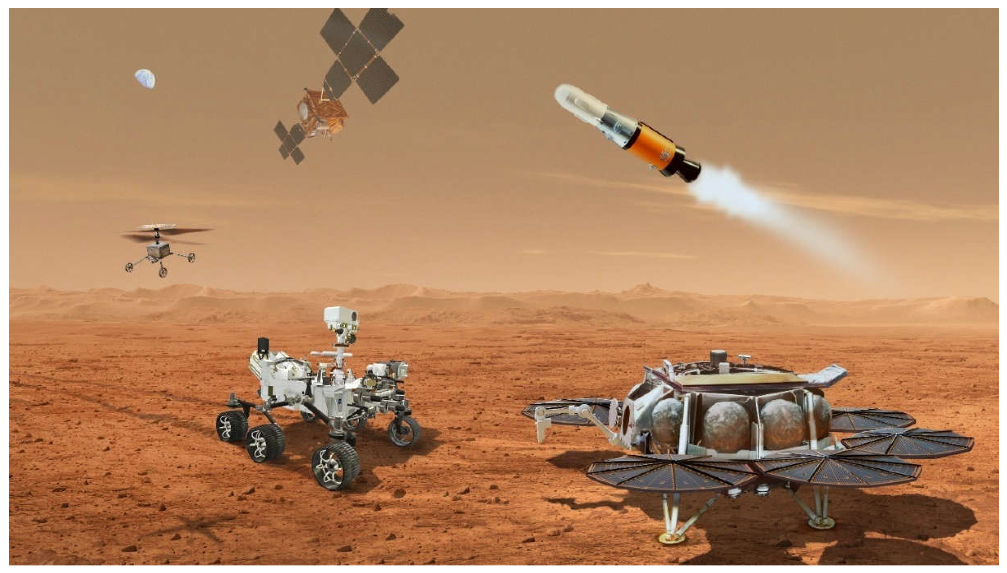
The launch, landing and Mars surface operations of the Perseverance rover are just the initial steps of the first phase of the NASA and European Space Agency (ESA) Mars Sample Return (MSR) campaign. The goal of the MSR campaign is to collect scientifically interesting samples from the Martian surface and return them to Earth for further study in terrestrial laboratories. Of particular interest for return are samples to help us understand the history of liquid water on Mars as well as its habitability in the distant past. Three major spacecraft components make up the current MSR campaign design: the Perseverance Mars rover currently operating, the Sample Retrieval Lander (SRL) and the Earth Return Orbiter (ERO). See
Figure 1 for an artist’s rendition of the MSR campaign’s major components.
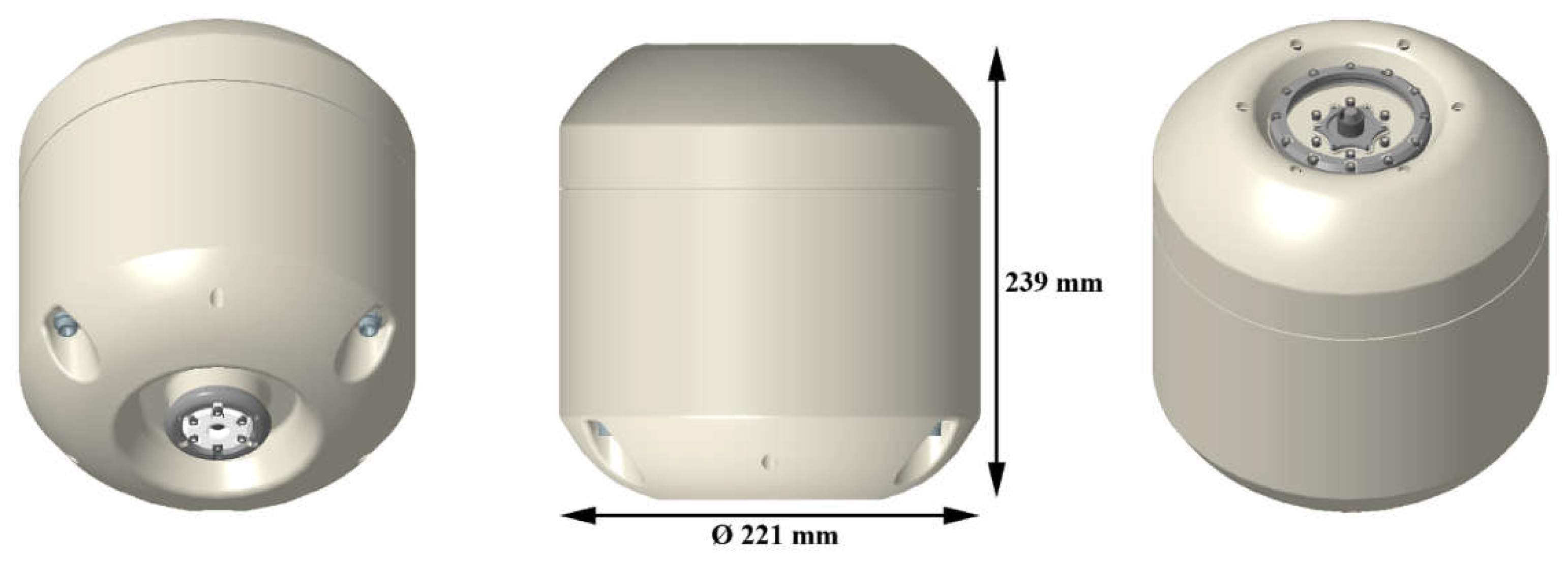
The role of the SRL spacecraft is to land near the Perseverance rover on Mars, collect the Martian sample and witness tubes acquired by Perseverance and launch those samples into Mars orbit. The nominal plan is for the Perseverance rover to deliver the sample tubes to the SRL to put them within reach of the ESA-provided Sample Transfer Arm. This arm will load the sample tubes, one at a time, into the Orbiting Sample (OS) container which sits atop the Mars Ascent Vehicle (MAV). After the OS is loaded with samples the MAV launches from the SRL and inserts the sample container into Mars orbit. The OS container is approximately 239 mm in length and 221 mm in diameter, similar in shape (but smaller in size) to a commercially available propane tank (see
Figure 2). It can hold as many as 30 titanium sample tubes from Perseverance. In the event that the Perseverance rover cannot deliver its samples to the SRL, the SRL also will deliver to the Martian surface two helicopters that can be used to retrieve the samples that Perseverance has cached on the surface. These will be similar in design to the Mars helicopter that successfully flew on Mars for the first time on 19 April 2021 [
2].
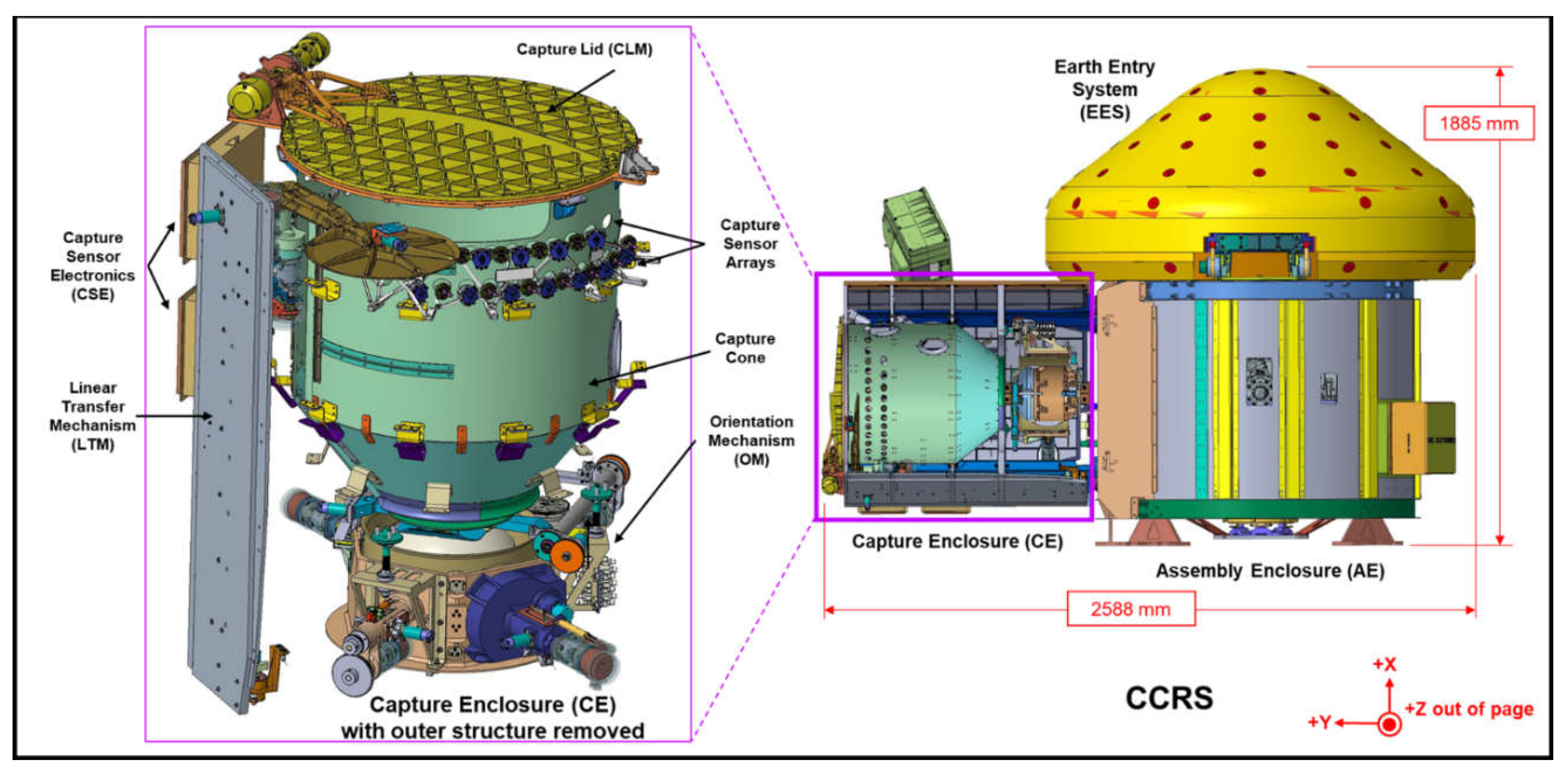
After the OS separates from the MAV and is inserted into Mars orbit, the MSR ERO spacecraft will rendezvous with the OS and capture it using part of its payload called the Capture, Containment and Return System (CCRS) (see
Figure 3). The ERO spacecraft as well as the ERO launch vehicle are being provided by ESA. CCRS is being provided by NASA’s Goddard Space Flight Center (GSFC).
After the OS is captured and prepared for delivery to Earth, ERO will leave Mars orbit on an Earth-return trajectory to release the CCRS Earth Entry System (EES). The EES will enter Earth’s atmosphere and impact Earth’s surface at the EES terminal velocity within the Utah Test and Training Range (UTTR) near Dugway, Utah. After landing in Utah the Mars samples will be transported to the NASA Johnson Space Center for curation before they are shared with other institutions around the world.
The primary CCRS operations begin after the OS container is inserted into Mars orbit. The ERO targets and rendezvous with the orbiting OS and maneuvers to align the OS orbital trajectory with the centerline of the CCRS capture cone, approaching the OS with a large enough closing velocity to overtake it. CCRS then performs a series of functions to capture the OS within its interior.
First, the CCRS capture lid is commanded open to expose the capture cone to space. Then, upon entry to CCRS, the OS trips optical capture sensors which trigger a rotation of the linear transfer mechanism (LTM) into position within the cone’s interior. The LTM then sweeps/pushes the OS to a captured reference position within an orientation mechanism at the end of the capture cone.
After OS capture, the CCRS begins a choreographed series of back-and-forth steps between sub-systems to sterilize the OS exterior, attach a lid assembly to the OS base and move the OS out of the CCRS capture enclosure volume and into the assembly enclosure using a rotation and transfer mechanism. Finally, the rotation and transfer mechanism loads the OS into the EES and closes out the EES for the return to Earth.
Before the rotation and transfer mechanism can mate the lid assembly to the OS, CCRS must determine if it is safe for the hardware to do so by confirming proper OS orientation. The purpose of the vision system is to supply OS image telemetry to perform that critical inspection step.
2. Vision System Overview
The CCRS vision system is one of eleven CCRS sub-systems. The primary vision system objective is to acquire images of the OS container after it has been captured by the CCRS and held stationary with respect to the vision system within the CCRS orientation mechanism. Post-capture OS images will allow CCRS operators on the ground to discern the orientation of the OS prior to sterilization and processing for Earth return. CCRS mechanical constraints only allow the OS to be held in the orientation mechanism in one of two orientations. If the vision system images reveal that the OS is in the wrong orientation for further processing by CCRS, then the orientation mechanism will rotate the OS 180° and the vision system will acquire additional images to determine that the reorientation was successfully completed.
In addition to its primary function the vision system can also provide supplementary information in support of other CCRS operations. For instance, if the LTM funneling process does not successfully deliver the OS to the orientation mechanism, then vision system images can provide situational awareness to inform contingency operations. The vision system can also provide telemetry that the ultraviolet (UV) illumination system is operational prior to OS capture [
3]. Although the vision system cannot directly detect the 280 nm ultraviolet radiation, it is sensitive enough to image the secondary visible illumination generated by UV fluorescence from certain CCRS surfaces.
The CCRS vision system architecture is based upon cameras using two-dimensional, silicon detector arrays with fixed-focus, refractive lenses and an illumination system that utilizes broadband light emitting diodes (LED). Similar types of imaging systems have been successfully operating at Mars since 1997 [
4,
5] and LED-based illumination systems were flight qualified for Mars conditions shortly thereafter [
6,
7].
The CCRS vision system consists of two camera heads and two illumination modules. Only one camera is required to fulfill the vision system’s operational goals but two are included for full system redundancy. Similarly, only one illumination module is required to take satisfactory images of the OS container but a second is included for full redundancy. The illumination modules are wired in a distributed manner such that any single or double system failure (except for double-fault cases where both cameras become inoperable or power is lost to both the primary and redundant electronics) will not degrade vision system performance. This arrangement is also resilient to roughly half of the possible triple failure modes, producing images that, though degraded, still meet requirements.
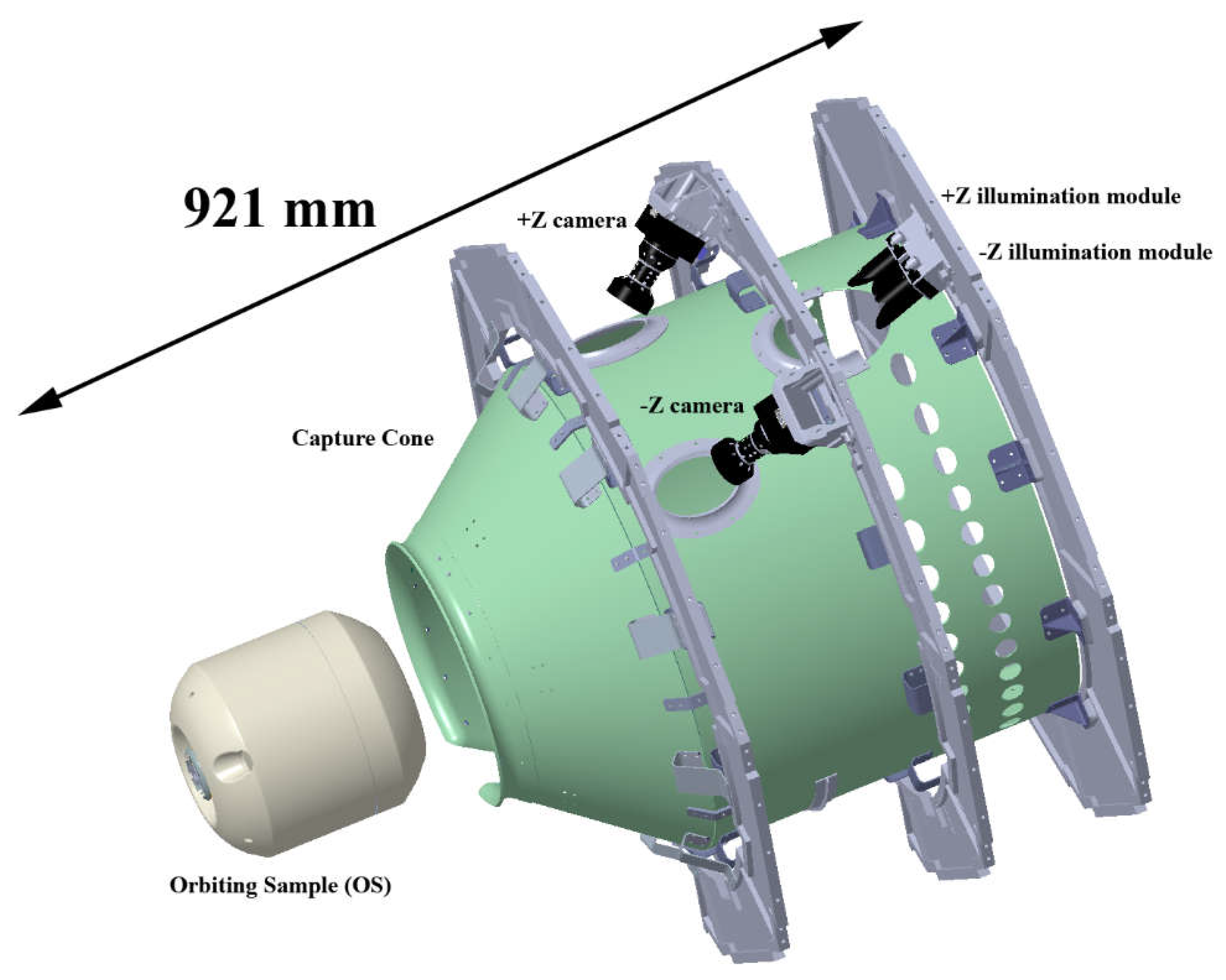
All the vision system components are located within the CCRS interior and mounted via bracketry to the capture cone bulkheads. Portholes within the capture cone provide lines of sight to the post-capture OS container and allow light from the illumination modules to illuminate the OS. Each camera has a dedicated porthole whereas the pair of illumination modules share a single large porthole. See
Figure 4 for an illustration of the vision system location within CCRS.
CCRS vision system optical performance is inextricably linked to the OS container’s external optical properties, specifically the optical properties of the container endcaps, as well as the CCRS interior ambient lighting conditions. Due to the immaturity of the CCRS mechanical and thermal blanket closeout design and uncertainties regarding spacecraft-to-sun vectors during on-orbit operations, the minimum ambient light level within the CCRS interior has yet to be bounded. In response we have designed the vision system to function properly with or without the presence of ambient light coming directly from the Sun or reflected from the Martian disk. We initially considered near-infrared and thermal infrared imaging solutions within the vision system design trade space. We did not choose that approach due to cost and schedule constraints as well the much greater spaceflight heritage offered by visible-light imagers.
To take advantage of current camera designs that have spaceflight heritage we designed our system around camera offerings from industry and academic sources and developed a new, custom illumination system to enable any such camera to acquire high-fidelity OS images. To do this prior to the completion of the OS design we developed optical property requirements for the OS container endcaps which the OS team considered as part of the OS design.
The first optical property we specified for the OS container endcaps was for their bidirectional reflectance distribution functions (BRDF) to lie within the range shown in Equation (1) over the 400-900 nm wavelength range and angles of incidence and reflectance,
θi and
θr, respectively.
This BRDF specification allowed for a broad range of OS endcap surface treatments for the OS design team to consider. At the high end, the OS endcap reflectivity is allowed to be highly specular (31 times more reflective than an ideal Lambertian reflector) and at the low end its reflectance can be just 63% that of an ideal Lambertian reflector. For the vision system we used these agreed-to BRDF limits to specify the range of acceptable illumination levels for the illumination system based on typical sensitivities for flight-heritage cameras and the illumination module-to-OS distances.
The second optical property we specified for the OS container endcaps was for individual and localized surface features to have a BRDF, BRDF
f, that differs from the surrounding surface BRDF over the 400-900 nm wavelength range by at least 25% as described by Equation (2).
This OS contrast requirement ensured that whatever camera we selected, we would be imaging a scene with discernible features and not just an object that while detected as being present (by meeting the specification in Equation 1) would be devoid of resolvable features. We defined the OS feature contrast in this manner so that we could use it directly to predict camera system performance using modulation transfer function (MTF) values. During initial development we required that OS contrasting features be at least 5 mm in size so that the vision system cameras could resolve them. Due to the viewing angles, OS topography and feature locations this meant that the cameras needed to resolve detail ~3 mm or larger. We will show in
Section 5 of this paper that now that the OS design is mature, we are able to determine that the OS endcap surface geometry by itself provides enough diversity in shape and large enough gradients in local surface slopes that shadows and shading are easily resolvable by the CCRS vision system even if individual features have the same BRDF as the background material.
Based on these two general reflective properties of the OS endcaps we developed optical requirements for both the vision cameras and the illumination modules and flowed them to the individual components. These will be discussed further in
Section 4.1 and 4.2.
For radiometric requirements we use photometric units for illuminance and luminance in place of radiometric units (e.g. Watts or photons) for irradiance and radiance. We did this due to three practical considerations. First, the vision system is intended to operate over a broad portion of the visible spectrum. Specifying irradiance and radiance over a broad wavelength range using radiometric units would also require an accompanying description of the applicable wavelength range as well as restrictions or descriptions on how the Watts or photons can be concentrated or distributed throughout the spectrum. Photometric units, although not perfectly constrained, are standardized with respect to a well-known and defined response curve. They do not require an accompanying ad hoc and elaborate spectral definition within the specification to eliminate ambiguity on where the optical power can fall on the spectrum. Second, most commercially available calibrated detectors that operate over the entire visible wavelength band are calibrated in photometric units of lux (or lumens/m2). Third, most (if not all) commercially available broadband LEDs are specified in terms of their total photometric output. By working entirely in photometric units we eliminate the errors, approximations and assumptions we would need to introduce in order to work with the absolute radiometric units that we typically work with on spacecraft optical instrumentation.
5. Vision System Performance
To assess the performance of the cameras and illumination modules functioning together as a unified CCRS sub-system we completed a comprehensive optical test and analysis program. The activities included: optical characterization of CCRS surface treatments, laboratory testing, non-sequential ray tracing and system modeling using higher-level languages such as Python.
In our experience this level of effort is unprecedented when compared to the development of optical systems for other planetary missions. We believe in the necessity of this activity given the criticality of the CCRS operation in the greater MSR campaign as well as the complicated imaging scene created by the captured OS and the CCRS interior. Relying on first-order calculations or depending upon scene simplifications is useful and expedient to develop component-level specifications but inadequate for verifying vision system performance in the unique CCRS environment. Discovering inadequate vision system performance during the CCRS-level integration and test phase would jeopardize our ability to launch on schedule – an unacceptable risk. Through our extensive test and analysis program we have determined that the flight system design will easily meet the CCRS on-orbit operational goals with significant margin. The sections that follow provide the basis for this conclusion.
5.1. Reflectivity and Scattering Measurements
Unlike our typical experience with planetary mission imaging systems, everything we plan to observe with the CCRS vision system will be manufactured. The only naturally occurring material we may image is contamination on the OS exterior. This provides both a challenge and an opportunity. The challenging aspect is that fabricated components are likely to have much more disparate reflectance properties than objects that appear in nature, potentially requiring a much more flexible imaging system than otherwise would be required. The advantage is that we can measure proposed MSR and CCRS surface properties to inform the selection of surface finishes as well as develop highly accurate predictions of vision system performance. To address both of these aspects we initiated a comprehensive optical characterization campaign of MSR and CCRS surface finishes relevant to the vision system.
Characterization of MSR and CCRS surface finish samples was performed at the Goddard Space Flight Center’s (GSFC) Diffuser Calibration Laboratory’s (DCL) optical scatterometer [
18]. The DCL is a secondary calibration facility with radiometric calibration measurement capabilities traceable to those made in the primary facility located at the National Institute of Standards and Technology (NIST). The scatterometer is located in a class ISO7 cleanroom. It can be used for BRDF and/or BTDF (bidirectional transmission distribution function) measurements in both in-plane and out-of-plane modes. The setup is modifiable to address the requirements of each project. The main configuration of the optical table includes the following components: an Energetiq EQ99 light source, a monochromator, tunable coherent sources, a supercontinuum white laser and an optical parametric oscillator system. Additional sources, polarization analyzers and filters can be connected to the setup depending on project requirements. Three detectors are available depending on the spectral range of interest: ultraviolet-enhanced silicon from 250 nm to 900 nm, indium gallium arsenide from 900 nm to 1700 nm and extended indium gallium arsenide from 1700 nm to 2500 nm.
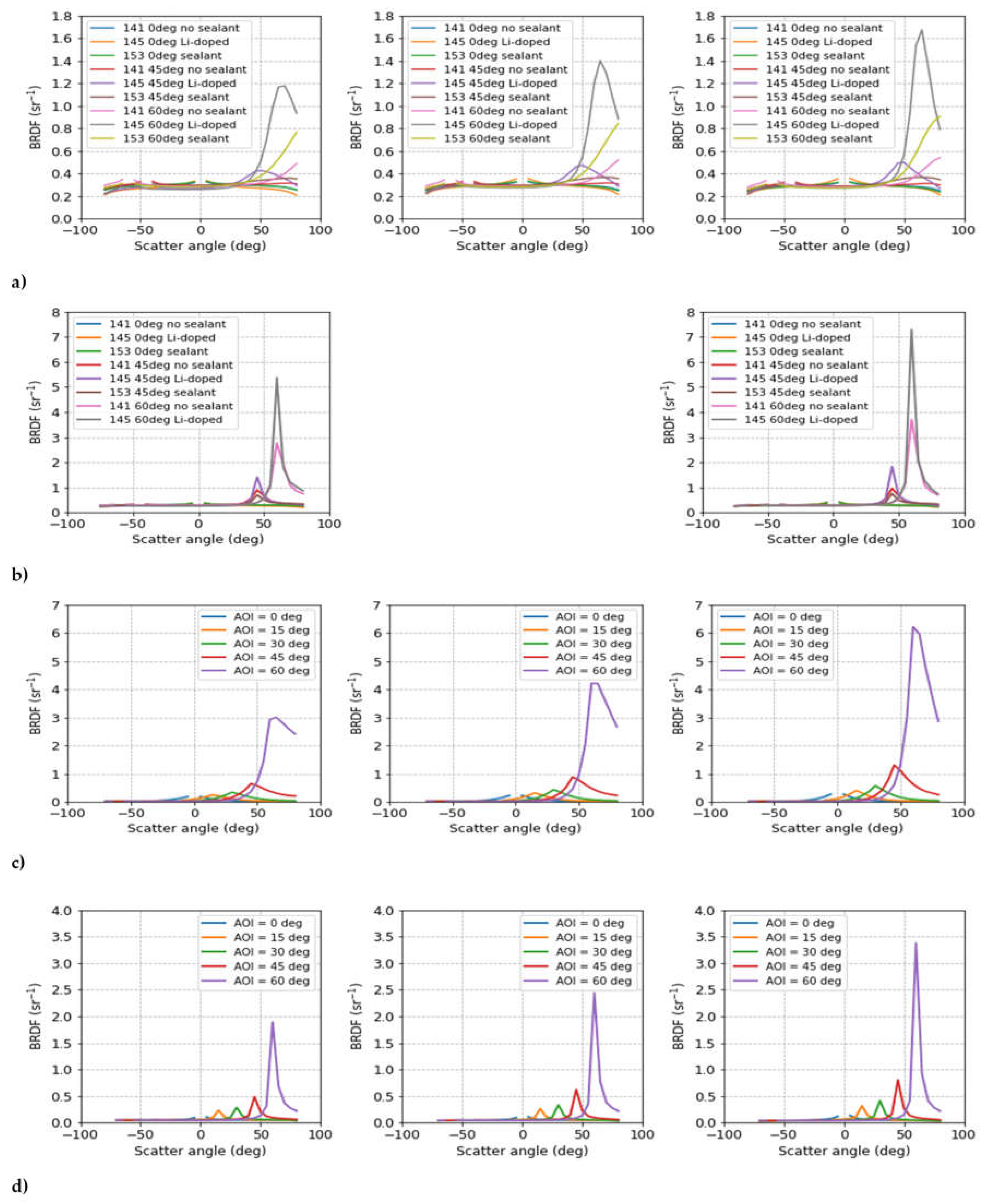
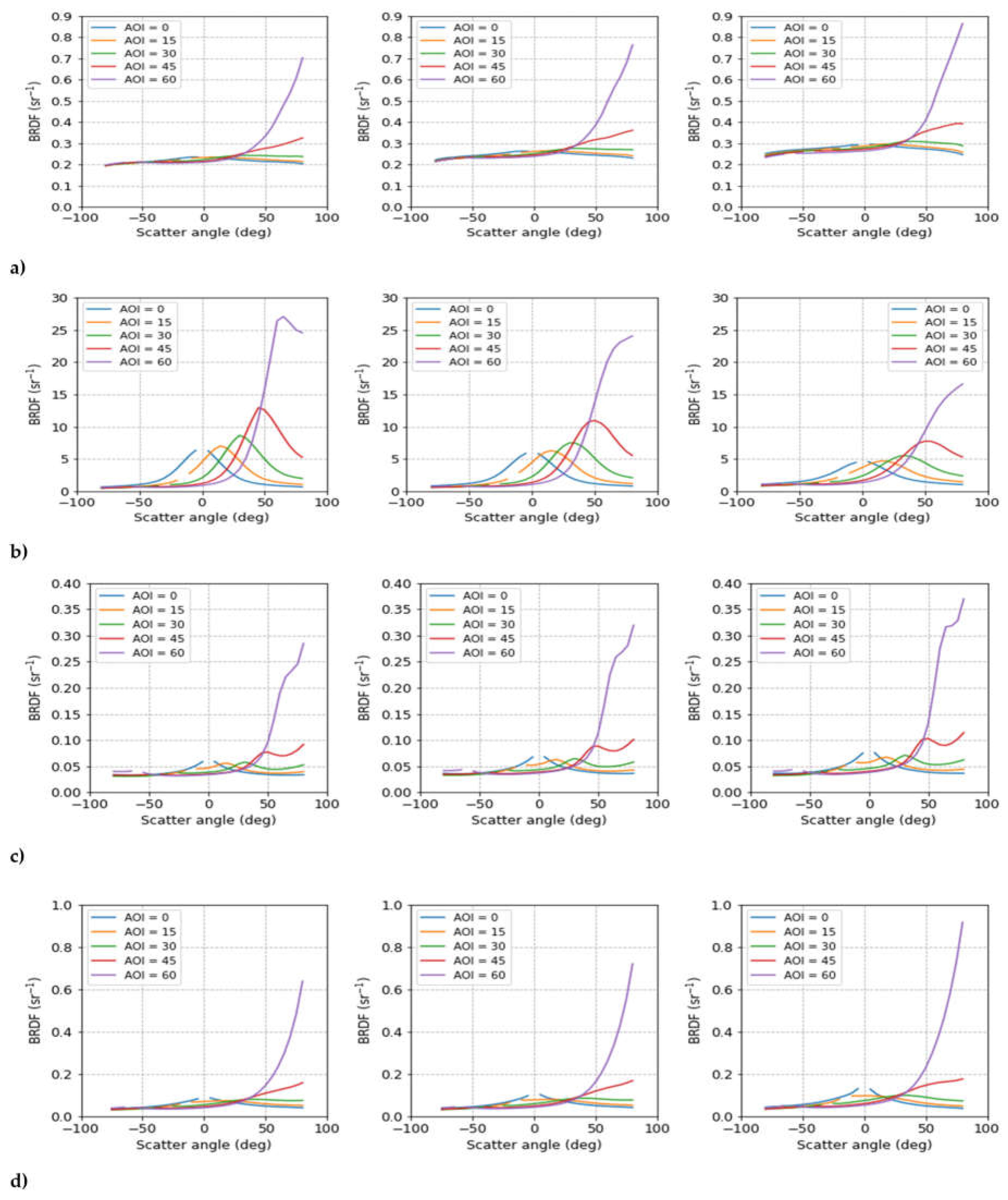
We typically characterized the MSR and CCRS surface finish test coupons at 440 nm, 550 nm and 700 nm. BRDF measurements were made at 0°, 15°, 30°, 45° and 60° incident angles over scatter angles of -80° to 80° in increments of 5°. Total hemispherical reflectance was also measured using a Perkin-Elmer 1050 spectrometer equipped with a 150 mm diameter integrating sphere. A summary of the materials tested is provided in
Table 6. A summary of measurements is provided in
Figure 33 and
Figure 34.
5.1. Laboratory Results
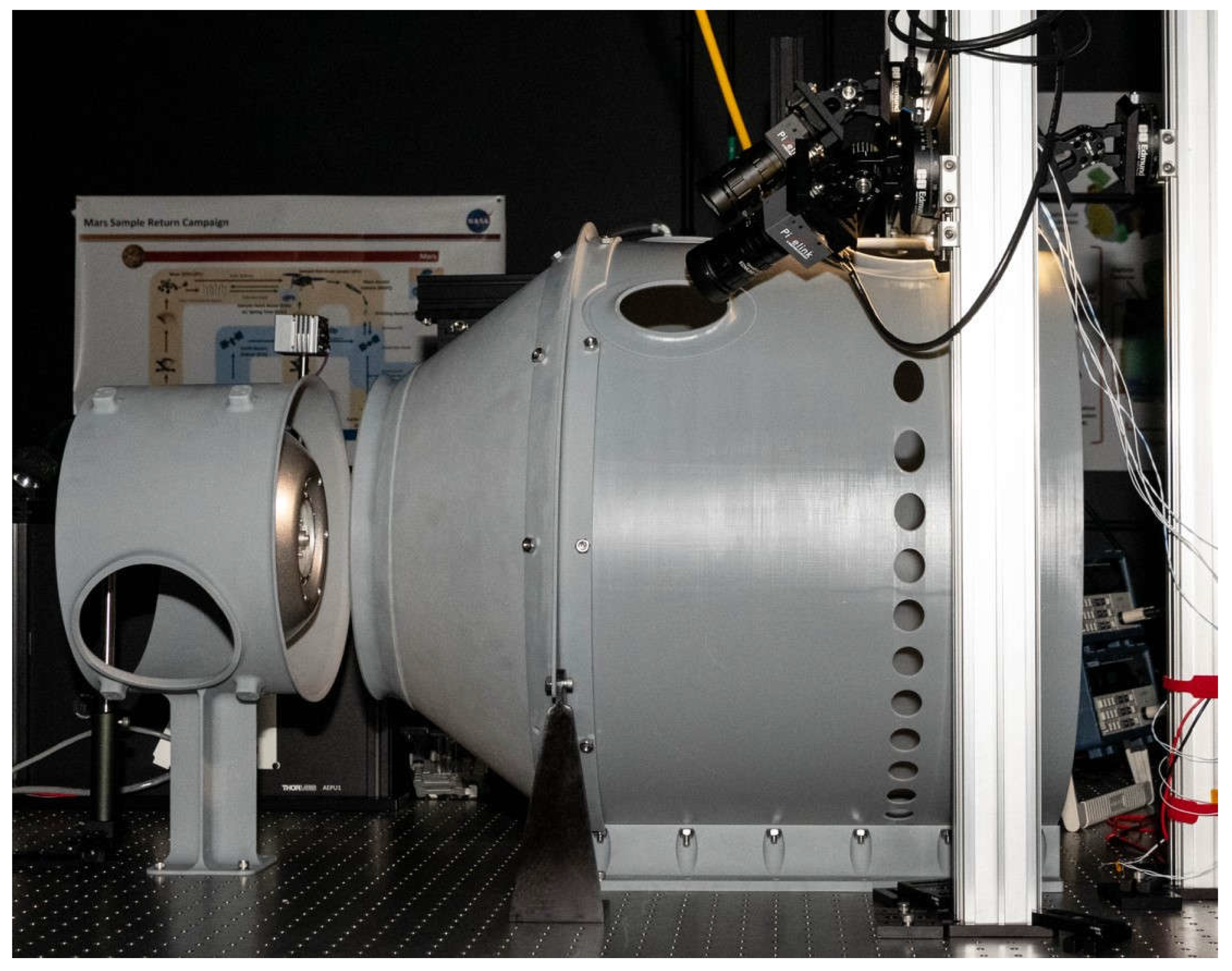
To assess imaging performance we constructed a vision system laboratory testbed to support component and system level optical testing. It is capable of rapidly producing high fidelity images in geometries and conditions comparable to CCRS. We use it to predict system performance under a wide range of scenarios and to cross-check computational models. The system level testbed is composed of off-the-shelf components, engineering development units (EDU), and custom 3D printed parts. See
Figure 35.
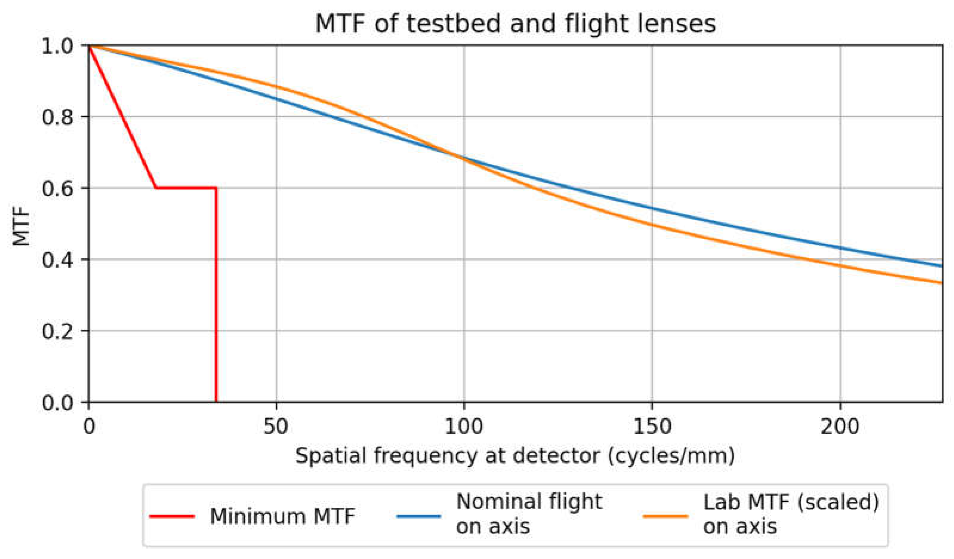
The testbed imaging system consists of two PixelLink Color 20 Mpx 1” 12-bit sensor cameras with Edmund Optics 12 mm TECHSPEC HP Series fixed focal length lenses set to F/3.5. This system has higher resolution, better signal-to-noise (SNR>80), larger FOV, and a smaller instantaneous field of view than the assumed flight system, allowing us to degrade and resample images in post processing to match specific flight system candidates. Postprocessing is further discussed in Section 5.4. The modulation transfer function (MTF) of the lens was measured using the commercially available Optikos LensCheck Finite Conjugate System [
19] and exceeds or closely matches the performance of the flight lens system (see
Figure 36). We confirmed the camera’s linear response with respect to luminance and exposure duration extends from at least 70 ms to 2000 ms using calibrated reflectance standards and a stable illumination source.
The testbed illumination system consists of two EDU LED boards with 3D-printed baffles designed to create the current flight design illumination footprint. The diffuse-white 3D printed specialty baffles mimic the diffuse bead blasted interior of the flight illumination system assembly baffles and shape the outgoing illumination pattern. The testbed illumination modules were operated at 25˚C and driven at 80 mA for each set of seven LEDs connected in series, then scaled in postprocessing to match worst case operating temperature and voltage conditions.
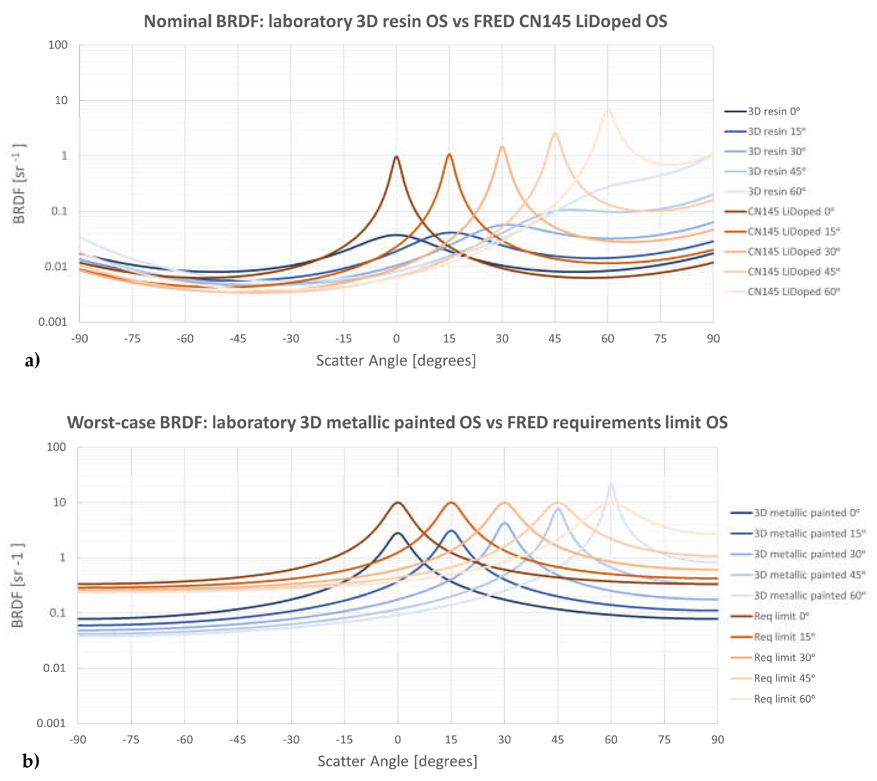
The testbed uses 3D printed OS lid and base endcaps. These are printed in house at GSFC to allow for rapid turnaround with OS design changes. The bare white resin material is used as a proxy of the baseline Li-doped, Ceranovis-145 OS coating. A shiny metallic spray paint coating is used as a proxy of the worst-case specular OS BRDF specification (See Equation 1). Since the testbed did not have access to endcaps with the flight materials and coatings, BRDF measurements were taken of bare and painted 3D printed coupons to determine how closely they matched the actual surfaces (see
Figure 37).
3D printed parts manufactured by Protolabs Inc. are used as proxies for the surrounding spacecraft infrastructure which substantially interacts with the vision system. Part structure is taken directly from flight assembly part models and altered only for attachment to the lab bench. BRDF measurements were not taken of these materials, as they are intended only for checks of obscuration and high level scatter effects, though visual comparison of the grey 3D printed pieces and the Teflon anodized Al 7075 assumed flight surfaces show roughly similar optical properties.
Laboratory cameras and illumination modules are manually aligned and located to within 0.5 mm and 0.5° at each build stage (i.e. camera location and pointing relative to the camera mount). The components mount via multiple layers of stages, with the propagated errors resulting in approximately 5 mm and 3° locational uncertainty relative to the lab origin. An image of the lab setup from 1 m behind the OS along the y-axis, taken with a known imaging system, was compared to a simulated image of the perfectly aligned setup. The comparison showed the alignment error to be less than ~5 mm. Final laboratory system level images agree in perspective with simulated non-sequential ray trace model images, further indicating that laboratory locational errors do not significantly impact our laboratory results and conclusions.
Illuminance is measured using an International Light Technology (ILT) 2400, SED033 sensor with a photopic filter at a spectral range of 400-700 nm. ILT calibrated the meter to ± 4.8% at 3215K using a standard quartz-tungsten-halogen source. Readout error at different color temperatures within 500K of 3215K falls within 1%. We used two independent cosine and photopic corrected light meters (Cooke cal-LIGHT 400) to perform an initial cross check of the ILT calibration; results agree on-axis to within 3% and off-axis to within 4%. In all the photometer calibration checks, we used the same LXZ1-4070 LED at 20˚C and powered it at 0.3 mA to illuminate the photometer 600 mm away. Additionally, the photometer calibration was verified against the GSFC photonics group’s Ocean Optics Spectrometer illuminated with a 4000K White LED Board; the ILT photometer is 12% lower than the spectrometer’s calibrated power value, likely due to the ILT photometer being calibrated for a different spectrum shape than the 4000K LEDs. We investigated the response of the photometer to oblique illumination and found its response deviates by ≥5% from that of an ideal radiometer when the angle of incidence is >20°. Removal of the diffuser head provides a photometer response that follows the theoretical cosine falloff out to an incidence angle of 45° to within 5% but invalidates the absolute photometric calibration.
For most laboratory work that involves cameras or the entire vision system we require our testbed images to be radiometrically calibrated in terms of luminance. To do this we image diffuse reflectance standards of varying reflectance and calibrate against the ILT photometer placed at the same location as the standard. The calibration setup is illuminated at normal incidence to the plane of the standard/photometer head and imaged at 13˚ off axis (as close as possible given the setup) to minimize cosine fall-off effects. We calculate a calibration factor for each red, green and blue image layer and apply it in postprocessing. Dark current images are taken for each unique set of images and applied in post processing.
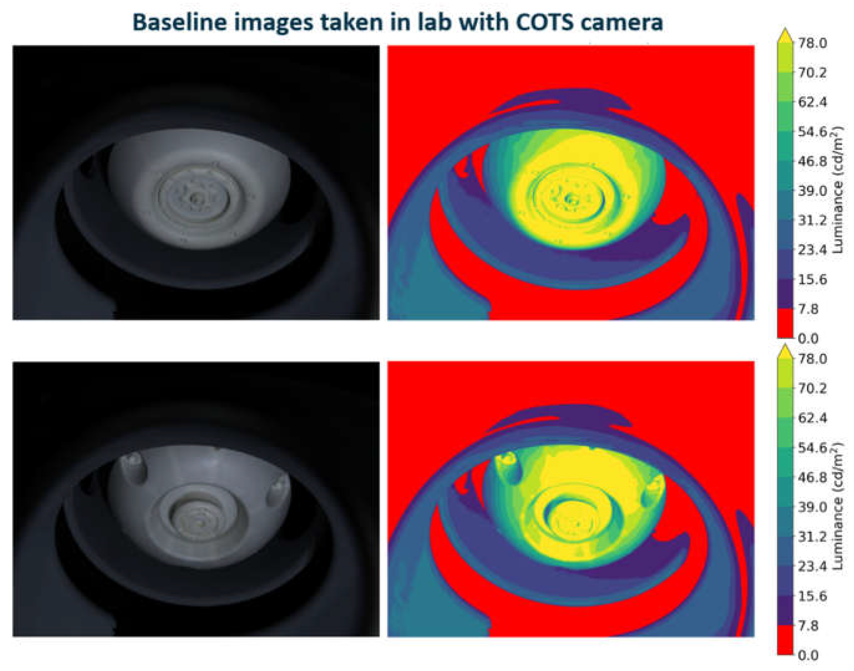
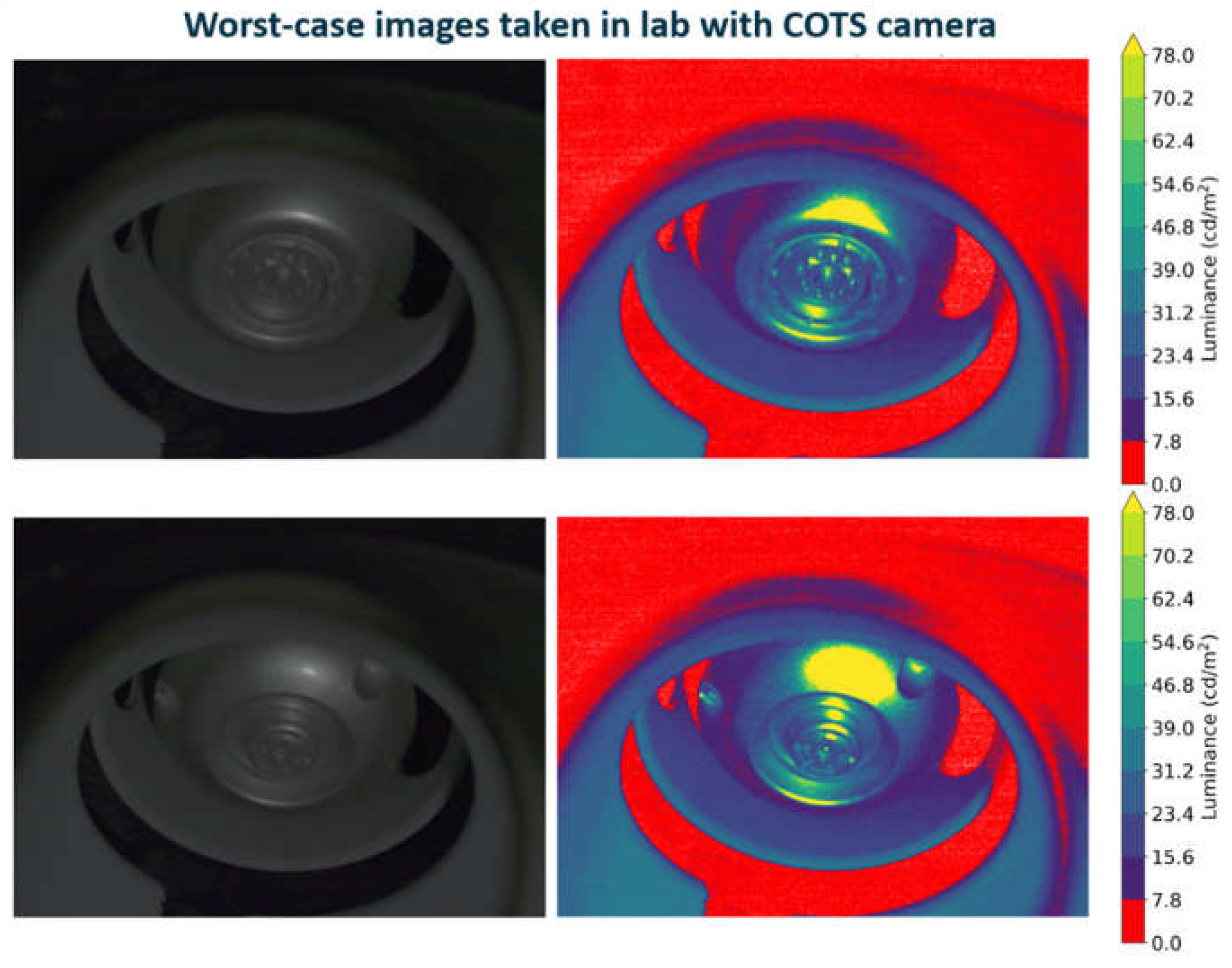
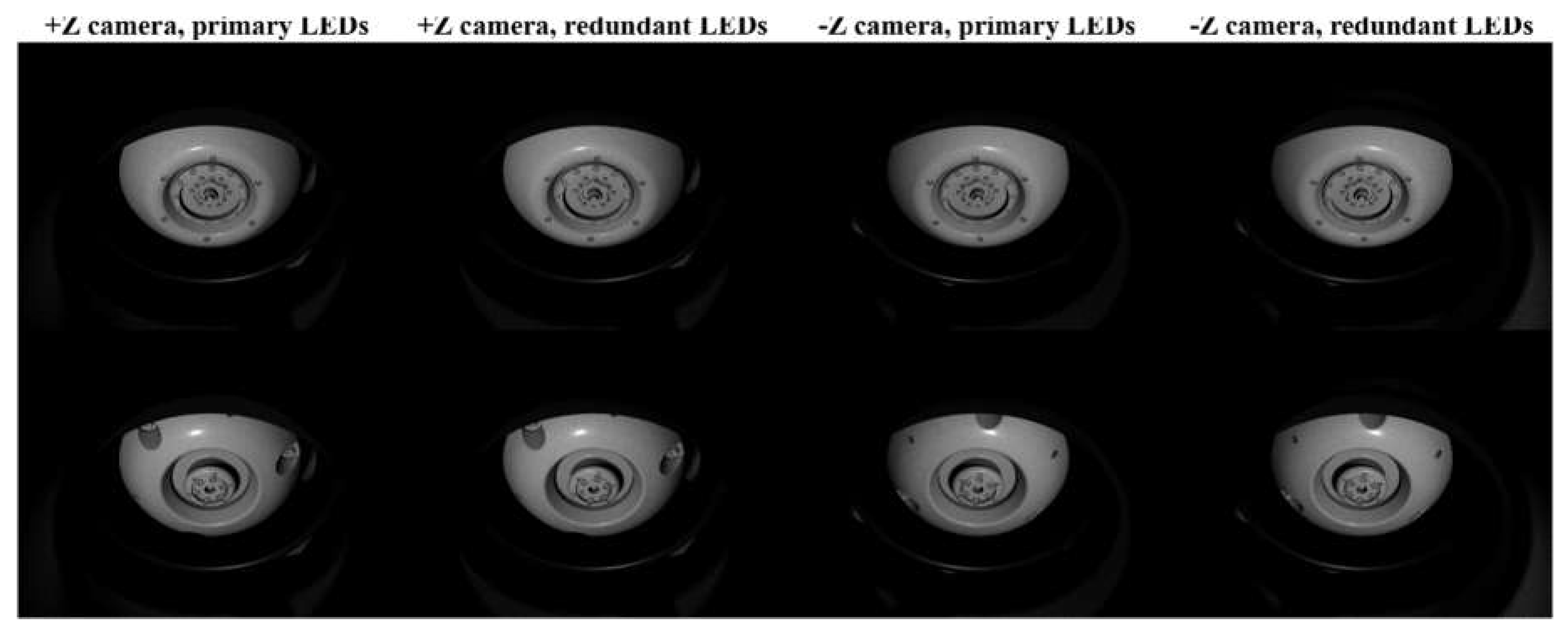
Our laboratory images of the current flight baseline and worst-case (i.e. all system performance characteristics at the edge of compliance) show compliance with requirements, see
Figure 38 and
Figure 39. The images provide clear distinguishability between the OS lid and base, and luminance requirements are met over the visible portion of the OS with key distinguishing features. Testbed images were also used to cross-check images generated completely by computer simulations (see
Section 5.3). These show agreement in overall views and endcap distinguishability, and agree in calibrated luminance to within ~10% (see
Section 5.3 for further discussion).
5.3. Non-Sequential Ray Trace Modeling
In addition to the laboratory testbed we constructed to assess vision system performance (Section 5.2), we built in parallel a non-sequential ray trace model of the CCRS vision system using the commercially available FRED Optimum software version 22.40.4 with the FREDmpc extension (Photon Engineering, Tucson, Arizona). We used this tool in conjunction with the laboratory testing to:
more accurately represent the CCRS surface finishes;
incorporate the optical performance of the actual lens design;
position and orientate components more accurately than the laboratory;
include CCRS components that cannot be economically or quickly created in the laboratory;
evaluate the performance of off-nominal conditions;
assess scattered light paths within the CCRS capture enclosure.
We created the model geometry primarily from STEP (Standard for the Exchange of Product Model Data) file exports of the CCRS and OS CAD designs developed in Creo (PTC, Boston, Massachusetts). CCRS components were simplified within Creo prior to export to contain only the optical information relevant to the non-sequential model.
Both camera models were built from information provided by MSSS. The refractive optical prescription was imported from a Zemax OpticStudio (Ansys, Canonsburg, Pennsylvania) model while the mechanical housing we built from information provided in a STEP file. The model validity was confirmed by: verifying the glass model for each lens; crosschecking dimensions with the original Zemax file; and then checking the skew ray intercepts at the detector and lens surfaces to confirm they match the Zemax results.
The illumination module representations were built from a combination of native FRED objects and STEP file exports from the illumination system CAD design. LED emission properties were modeled using a curve fit of the vendor’s beam apodization data and the total LED reported integrated light output in terms of lumens.
We assigned model optical properties based on measurements of hardware coupons or measurements of similar materials that have previously flown on spacecraft. The model surface properties are summarized in
Table 7. Optical properties that varied with incidence and exitance angle were modeled by fitting analytical forms of a combined Harvey-Shack and Lambertian model [
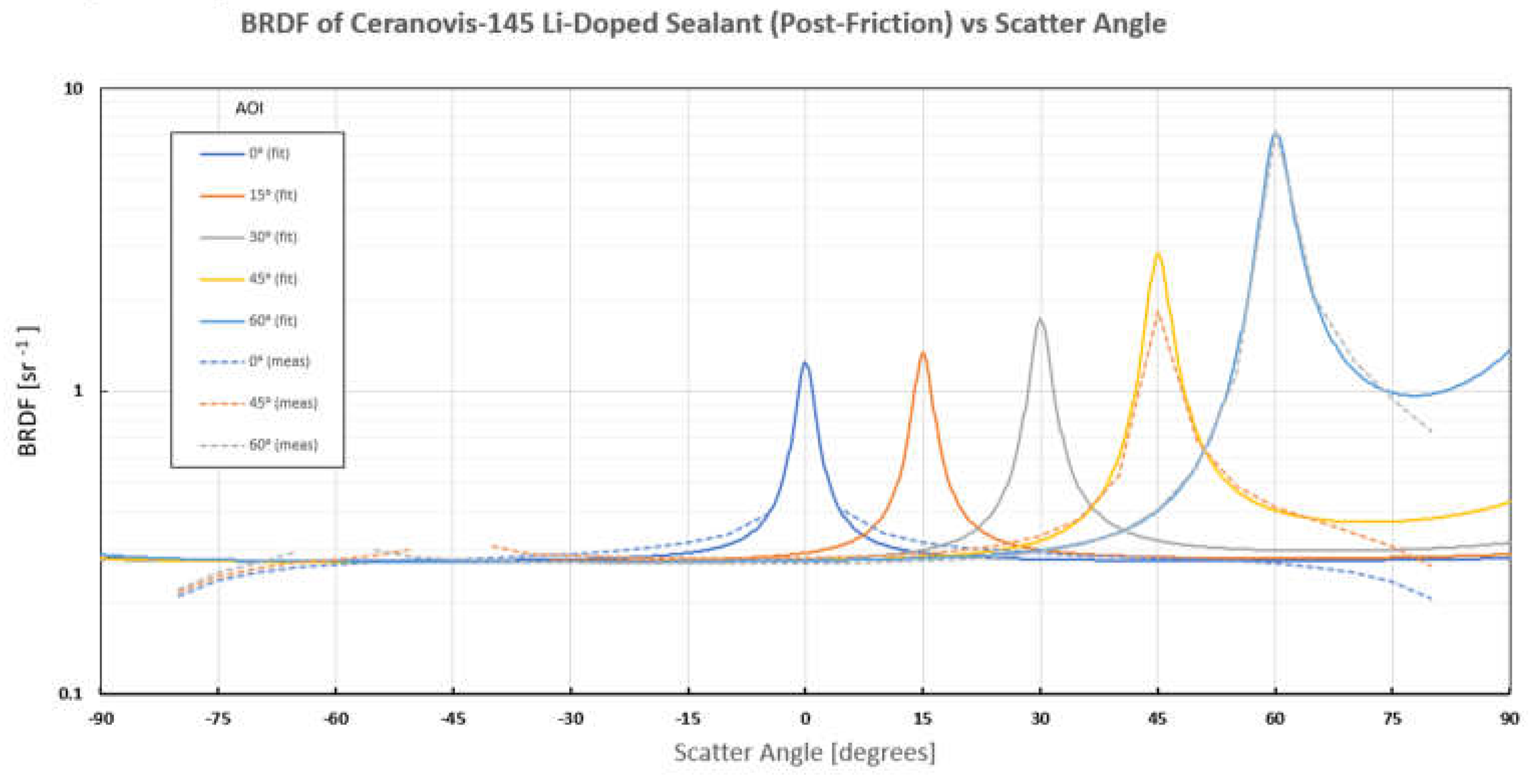
20] to the laboratory BRDF measurements. An example of the scatter model we used for the OS coating is shown in
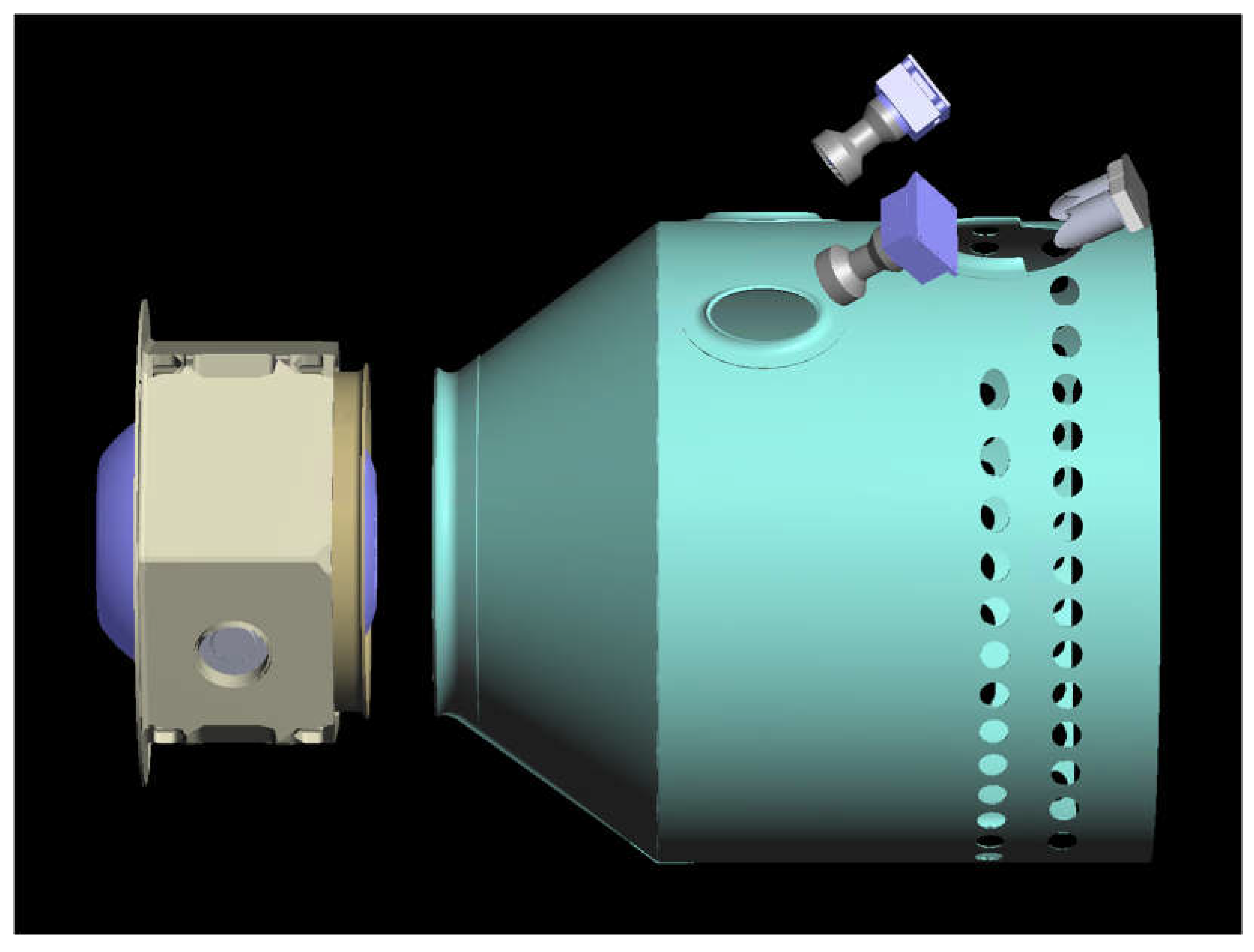
Figure 40. Views of the completed model are shown in
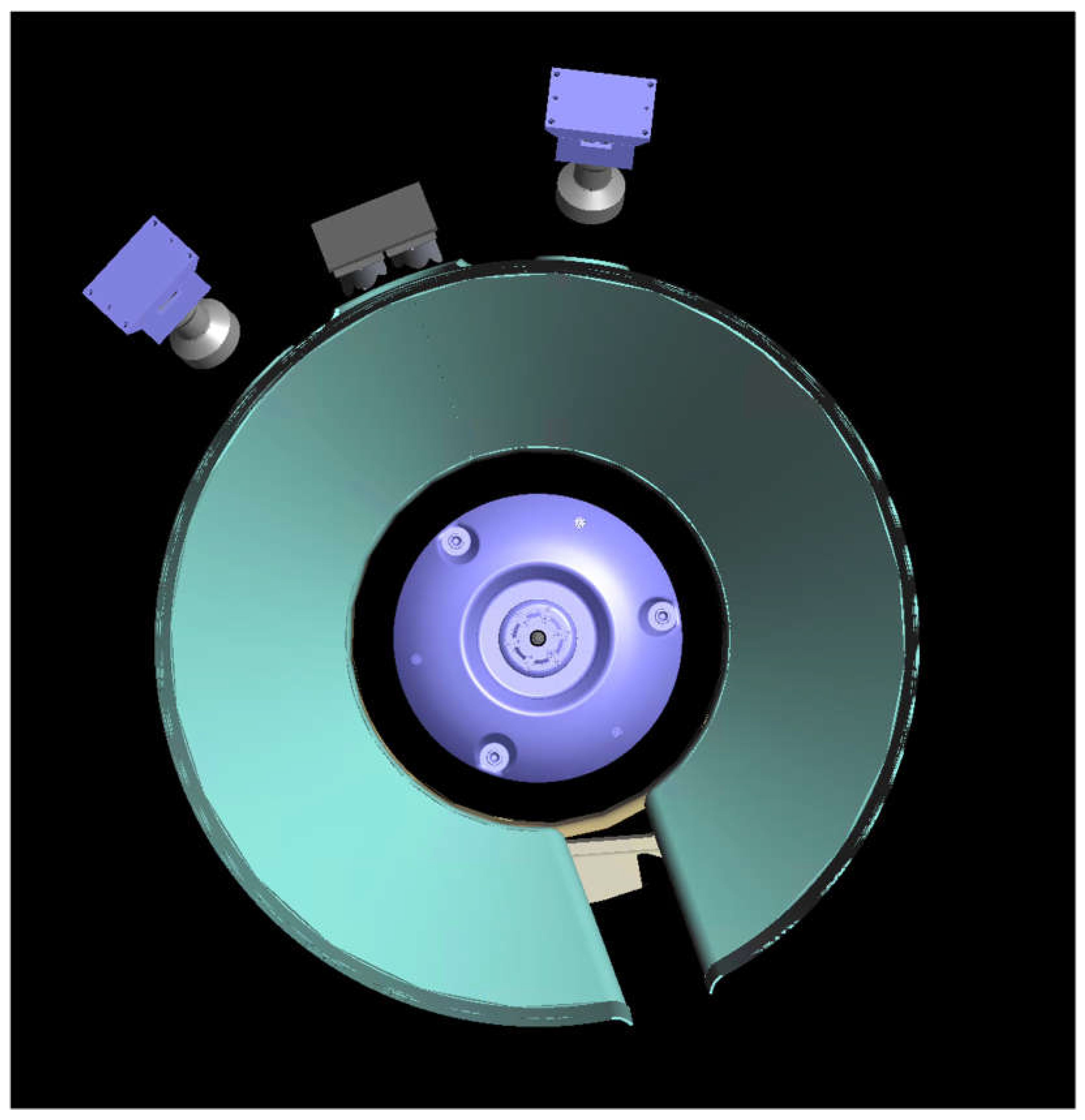
Figure 41 and
Figure 42.
We validated the radiometric accuracy of the non-sequential model by ray tracing a special case of the CCRS set up that we could also readily replicate in the laboratory. The test set up included just the cameras, illumination modules and a nominal OS base and lid. The LED light output in the model was set to match the current draw on the laboratory power supply. This initial crosscheck identified a small error in the laboratory calibration as well as a non-trivial calculation error in FRED. Through additional work we determined the FRED radiometric error only occurred when running ray trace calculations on the computer’s graphics processing unit (GPU). Subsequently we started running our FRED calculations on the computer’s central processing units (CPU) while the software vendor worked with the GPU vendor (NVIDIA) to correct the 522.30 NVIDIA driver issue. We also recalibrated all of our laboratory data. Even though the GPU-based calculations run 100 to 145 times faster than the CPU calculations we have not been able to validate the GPU calculations produce radiometrically accurate predictions and are avoiding that functionality for the time being. All of the results we present here come from calculations run on the CPU.
After correcting the laboratory and software errors, we find good radiometric agreement between the laboratory test results and the non-sequential model predictions. Within the areas of slowly varying luminance across the OS base and lid, the radiometric predictions typically agree to ~10% - about the level of agreement we would expect based on our photometer’s calibration uncertainty, our ability to measure and model the OS surface BRDF and the positional errors inherent in the laboratory set up (see
Figure 43).
To create nominal vision system performance predictions we set up the model geometry to match the nominal post-capture OS geometry of CCRS, including both possible OS capture orientations. Nominal surface properties (post-friction tested Ceranovis CN-14 with Li-doped sealant) are assigned to the OS (see
Table 7). We allow one level of ray splitting from each ray launched and up to eleven scatter rays per ray (i.e. up to eleven “children” rays can come from one “parent” ray). Importance sampling is implemented to force scattered rays to propagate toward one of the cameras while maintaining radiometric accuracy. 15.4 million rays with the same wavelength (700 nm) are launched in a single Monte Carlo run from either the primary or redundant set of LEDs and allowed to propagate and scatter until they reach a camera detector plane. This ray trace is repeated 250 times to improve the prediction statistics while keeping the ray trace dataset size below the computer memory cache limit. To improve the prediction statistics further we sum the detected energy over 8.8 µm x 8.8 µm pixels in the analysis plane (equivalent to 4x4 pixel spacing in the actual detector). In this way simulation signal-to-noise ratios (SNR) on the order of 20 or better can be achieved with only slight degradation in the prediction.
To generate the worst-case vision system performance predictions, to feed into the full vision system performance predictions of Section 5.4 we use the same settings and procedure as described above for the nominal conditions with two modifications. First, we switch the OS surface properties to match the worst-case specular BRDF described by Equation 1. Second, we position the OS as far away from the vision system as allowed by the CCRS capture tolerances and tilt the OS to the maximum tolerance in the most unfavorable orientation for viewing endcap features. Model results for both the worst-case and nominal conditions are presented in the following section (Section 5.4).
5.3. Full System Performance Predictions
Although both the laboratory testbed hardware and the non-sequential ray trace models are powerful tools for predicting the vision system performance, neither of them are able to include all the relevant effects that will determine the on-orbit vision system performance. Fully predicting the interplay between the light emitted from the illumination module LEDs, the reflection of that light off the OS and its passage through the camera lens to the detector plane where it generates signal electrons within the CCRS flight environment requires additional work. Here we describe the modeling techniques we use to turn the results from both the laboratory and the non-sequential ray trace tools into more accurate imaging performance predictions.
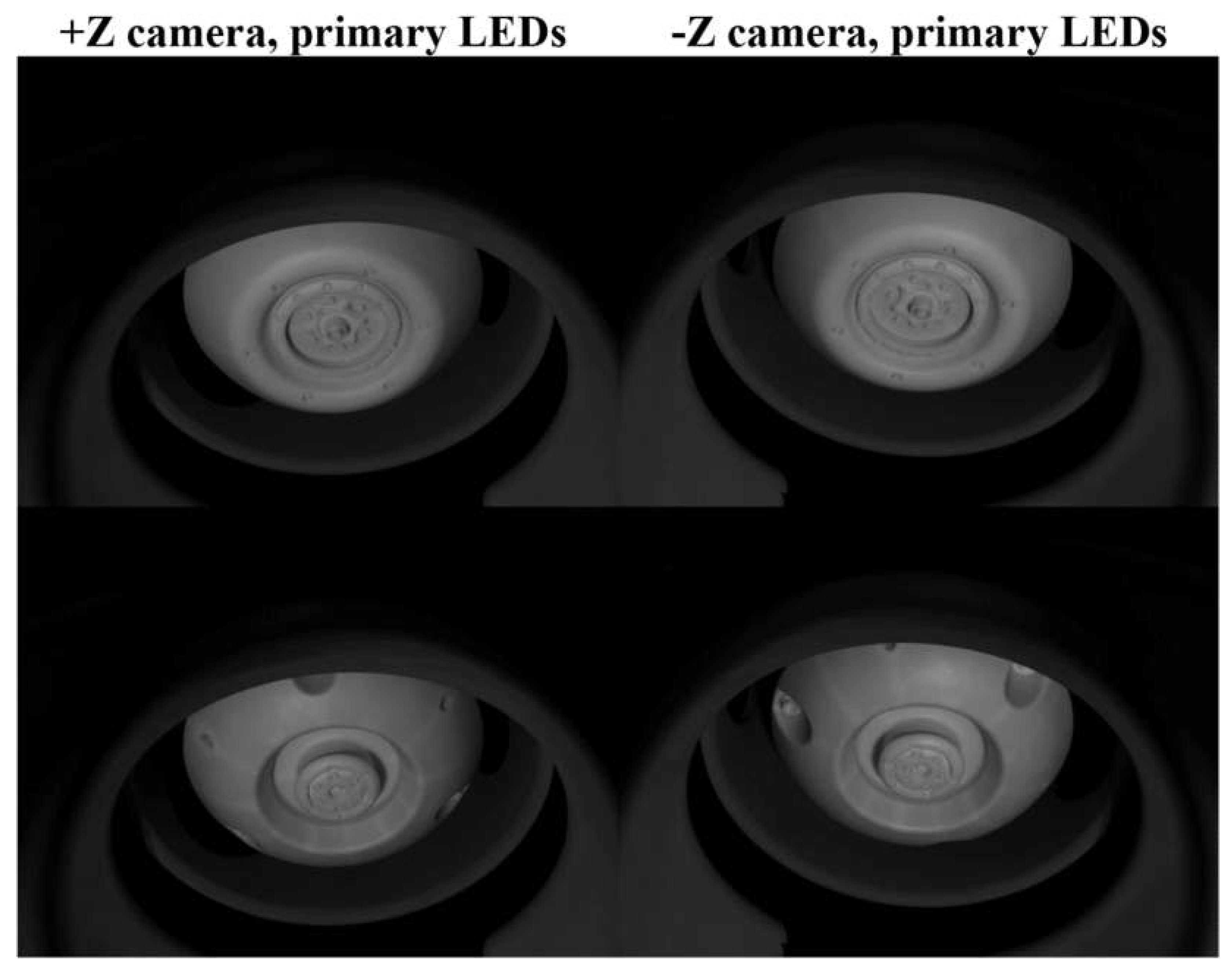
The laboratory testbed generates images with higher resolution and optical distortion that differs from the flight camera design. To correct this we use the Zemax optical model provided with the Edmund Optics lens and the flight model optical prescription provided by MSSS. We use these optical models to calculate the radial distance from the optical axis at the image plane corresponding to field angles into each camera. These curves are then used to map pixel coordinates of the COTS lens to the image space of the flight lens. We average the values from the COTS sensor pixels with mapped coordinates falling within a flight system pixel to produce image data matching the FOV and IFOV of the flight system. Interpolation is not required since the IFOV of the COTS camera is less than that of the flight camera. Using this approach we create the nominal performance predictions shown in
Figure 44 using the laboratory results.
Figure 44 shows that we can easily discriminate between the OS lid and base from vision system images. Based on the in-flight sensitivity of previous ECAM cameras [
9], these simulations are equivalent to a 0.2 s exposure with a 1X gain setting – well within our 1 s requirement. The results from the non-sequential ray trace model lead us to the same conclusion (see
Figure 45). Unlike the laboratory results, the FRED non-sequential ray trace model results do not require additional processing to faithfully represent nominal vision system performance. In fact, the FRED model’s image quality is already slightly degraded due to the use of detector pixels four times larger than the actual detector. In addition the simulated images have approximately three times more random noise than a well-exposed real image will have due to the Monte Carlo ray trace statistics. Even under these less-than-optimal conditions our non-sequential ray trace modeling predicts excellent vision system performance.
A feature to note in
Figure 44 and
Figure 45 is that the vision system cameras have a larger field of view than is required to image the OS endcaps and the cameras see portions of the capture cone exterior. This allows for large alignment tolerances on the camera installation and is due to ECAM lens availability and limitations on the size of the capture cone portholes. Also, a part of the capture cone flange obscures a small portion of the OS endcaps from the camera fields of view.
Unfortunately, we may encounter vision system manufacturing and assembly issues prior to launch or less than nominal conditions in flight that degrade the imaging performance predicted in
Figure 44 and
Figure 45. To verify that the vision system will meet its requirements under all off-nominal conditions we perform additional modeling to add the deleterious effects of: off-nominal OS alignment, specularly reflective OS endcaps, maximum lens contamination; worst-case lens performance and worst-case detector noise.
We model the worst-case OS by changing the nominal OS surface BRDF characteristics to the most specular allowed by Equation 1. Then we move the OS and tilt it into a post-capture tolerance extreme position that obscures more of the endcap from the cameras. This is all done in the FRED model described in
Section 5.3 and worst-case images are generated using the same procedure as for the nominal case. These worst-case images are then processed further to add image degradations caused by other effects.
To simulate particulate contamination on the first lens surface at the maximum level specified for the post-capture CCRS flight environment (0.02% areal coverage scattering ~0.05% of incident light) we convolve the worst-case images with a Mie scatter profile at normal incidence. Although we could have modeled this scatter caused by contamination with slightly higher fidelity in FRED, this simplified approach accounts for this effect with far less computation time.
To degrade the camera lens performance to the minimum level specified by the camera requirements we convolve the worst-case images with a significantly degraded point spread function (PSF) – one that just meets the minimum MTF requirement shown in
Figure 8. This worst-case PSF comes from a 1,000-case Monte Carlo analysis that allowed the lens parameters to vary randomly across a uniform distribution with the tolerances shown in
Table 8. These tolerances were significantly looser than the actual fabrication and assembly tolerances prescribed by MSSS. The resulting PSF was dominated by coma and just met the minimum MTF requirement.
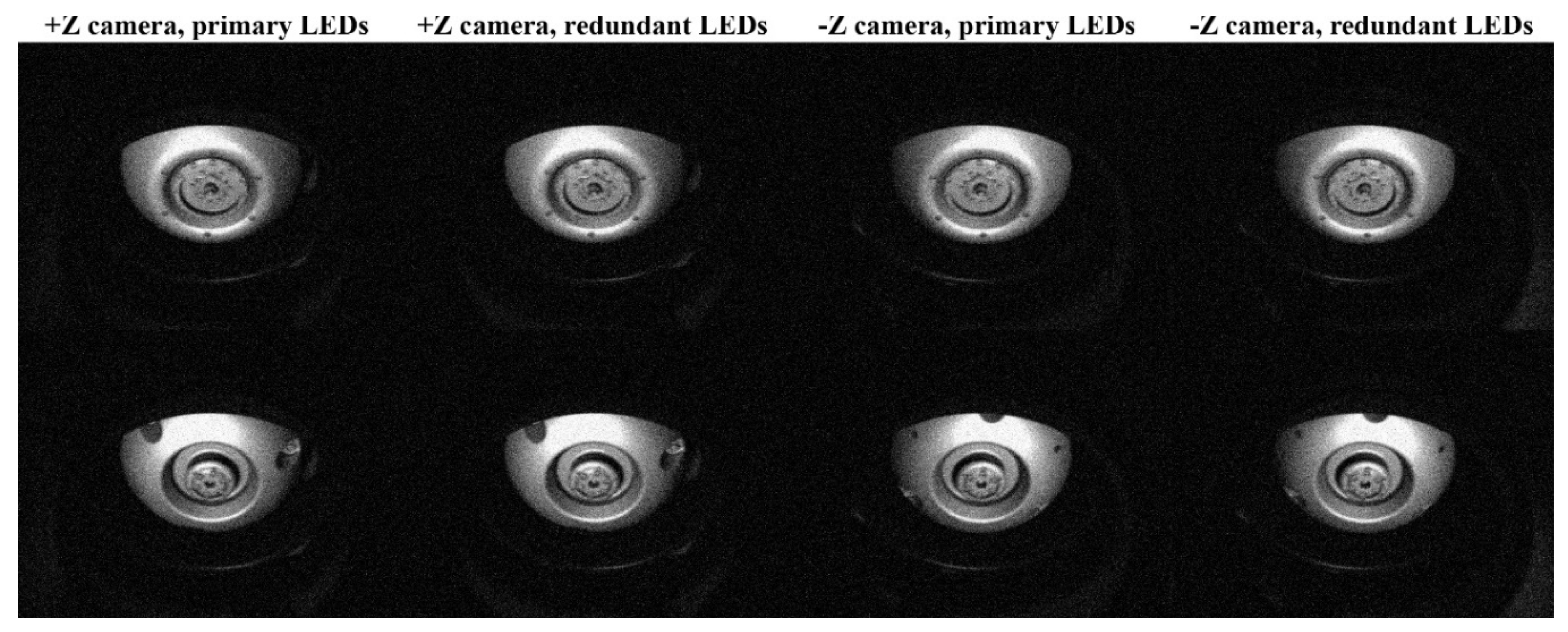
Finally, detector noise is added to the worst-case simulation to simulate images with a signal-to-noise ratio of ten. Noise is added by assigning to the images new pixel values drawn from normal distributions centered on the original pixel values with the standard deviation equal to the maximum pixel value divided by ten. The image predictions for all of these combined worst-case effects are shown in
Figure 46. These predictions show that even if all known effects combined together in the worst possible way, only one vision system image would be required to identify the OS post-capture orientation.
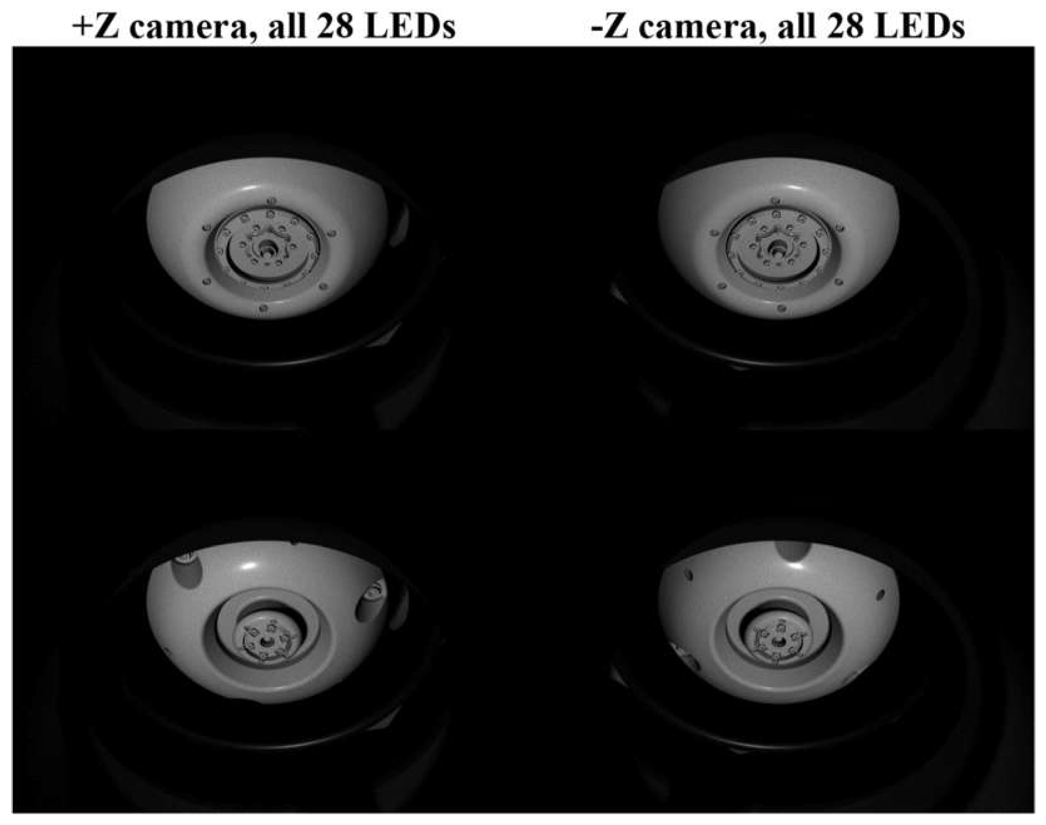
Although the nominal vision system operations concept plans for only 14 LEDs to illuminate the OS during image acquisition (from seven LEDs in each illumination module), the current baseline CCRS operations concept calls for powering on all 28 LEDs at once for the sake of operational efficiency.
Figure 47 shows the nominal vision system performance if this concept is followed. The image quality is almost indistinguishable from the 14 LED case (
Figure 45), slightly improves image uniformity and allows us to cut the exposure time (0.1 s) in half.
Author Contributions
Conceptualization, B.J. Bos, D.L. Donovan, J.I. Capone, C. Wang, M.A. Ravine, M. Caplinger, I. Orlowski, C. Sheng, R.A. Edison, D.A. Harvey, C.M. Yew and E.L. De Marco; methodology, B.J. Bos, R. Podgurski, J.I. Capone, B. Rizk J. Lauenstein, K.L. Ryder, M.J. Campola, D.E. Johnstone, W.J. Thomes, R.G. Schnurr, J.C. McCloskey, A.H. Le and B. Yang; software, J.I. Capone, T.C. Hardwick, R. Podgurski, K.C. Olsen, M.T. Hackett, E. Percy and E. Lee; validation, T.C. Hardwick, R. Podgurski and J.I. Capone; formal analysis, T.C. Hardwick, R. Podgurski and J.I. Capone; investigation, T.C. Hardwick, C. Wang, G.T. Georgiev, K.A. Washington, P. Coulter, E. Percy, L.Q. Vo, K.C. Olsen, B. Dizzon, L. Haseltine, C. Torisky, M. Han and B. Blonski; resources, B.J. Bos, D.E. Bell, R.R. Bousquet and E.M. Georgieva; data curation, B.J. Bos, D.L. Donovan, J.I. Capone, C. Wang, T.C. Hardwick, D.E. Bell, Y. Zhu, R. Podgurski, B. Rizk, G.T. Georgiev, M. Singer and S. Ioana; writing – original draft preparation, B.J. Bos, D.L. Donovan, J.I. Capone, C. Wang, T.C. Hardwick, D.E. Bell, Y. Zhu, R. Podgurski, B. Rizk, R.A. Edison, D.A. Harvey, C. Sheng, G.T. Georgiev, M. Caplinger and E. Lee; writing – review and editing, B.J. Bos, D.L. Donovan, J.I. Capone, C. Wang, T.C. Hardwick, D.E. Bell, Y. Zhu, R. Podgurski, B. Rizk, R.A. Edison, D.A. Harvey, C. Sheng, G.T. Georgiev, M. Caplinger and E. Lee; visualization, B.J. Bos, D.L. Donovan, J.I. Capone, C. Wang, T.C. Hardwick, D.E. Bell, Y. Zhu, R. Podgurski, B. Rizk, R.A. Edison, D.A. Harvey, C. Sheng, G.T. Georgiev, E.L. De Marco, M. Caplinger and E. Lee; supervision, B.J. Bos, E.M. Georgieva, C. Wang, Y. Zhu and D.E. Bell; project administration, B.J. Bos and D.E. Bell; funding acquisition, B.J. Bos. All authors have read and agreed to the published version of the manuscript.
Figure 1.
Artist’s rendition of the Mars Sample Return (MSR) campaign’s major components. In the lower left is the Perseverance Mars rover that successfully landed on Mars on 18 February 2021 and is currently acquiring up to 38 samples from the Mars surface and atmosphere. In the lower right is shown the Sample Retrieval Lander (SRL) which delivers to the Martian surface the Sample Transfer Arm and the Mars Ascent Vehicle (MAV) which is shown launching the Orbiting Sample (OS) container into Mars orbit. In the far left one of two SRL helicopters is shown which will be used as backup to retrieve cached sample tubes in case Perseverance experiences a failure prior to the arrival of the SRL. At the top is shown the Earth Return Orbiter (ERO) which will rendezvous with the OS container and capture it using the Capture, Containment and Return System (CCRS) that is included as part of its payload. After successfully capturing and processing the OS for Earth return, the ERO will leave Mars orbit and deliver the samples back to Earth.

Figure 2.
Conceptual computer aided design (CAD) views of the Orbiting Sample (OS) container as it appears in Mars orbit after release from the MAV (Mars Ascent Vehicle) showing an oblique view of the base endcap (left) and the lid endcap (right).
Figure 2.
Conceptual computer aided design (CAD) views of the Orbiting Sample (OS) container as it appears in Mars orbit after release from the MAV (Mars Ascent Vehicle) showing an oblique view of the base endcap (left) and the lid endcap (right).
Figure 3.
Conceptual computer aided design (CAD) views of the ERO (Earth Return Orbiter) Capture, Containment and Return System (CCRS) payload. The coordinate system axes shown in the lower right have their origins offset from the actual (0, 0, 0) vertex for clarity.
Figure 3.
Conceptual computer aided design (CAD) views of the ERO (Earth Return Orbiter) Capture, Containment and Return System (CCRS) payload. The coordinate system axes shown in the lower right have their origins offset from the actual (0, 0, 0) vertex for clarity.
Figure 4.
Simplified internal view of a portion of CCRS (capture enclosure) showing the location of the vision system with respect to the capture cone (pale green) and the post-capture OS (off white). Brackets mount the two vision system cameras and illumination modules to two different CCRS bulkheads. Views of the OS and apertures for illumination are provided by three portholes in the capture cone cylinder. Each camera has a dedicated porthole while the two illumination modules share one large porthole. The colors (black) shown for the vision system components are true-to-life whereas the colors applied to all the other components are for figure clarity. The orientation mechanism is not shown to make the post-capture OS position clearly visible.
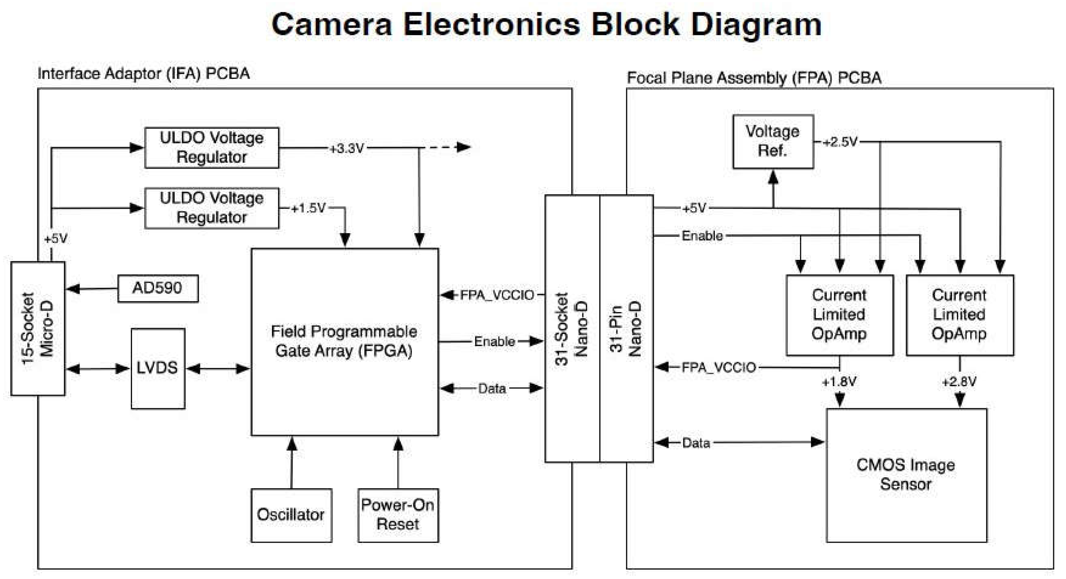
Figure 5.
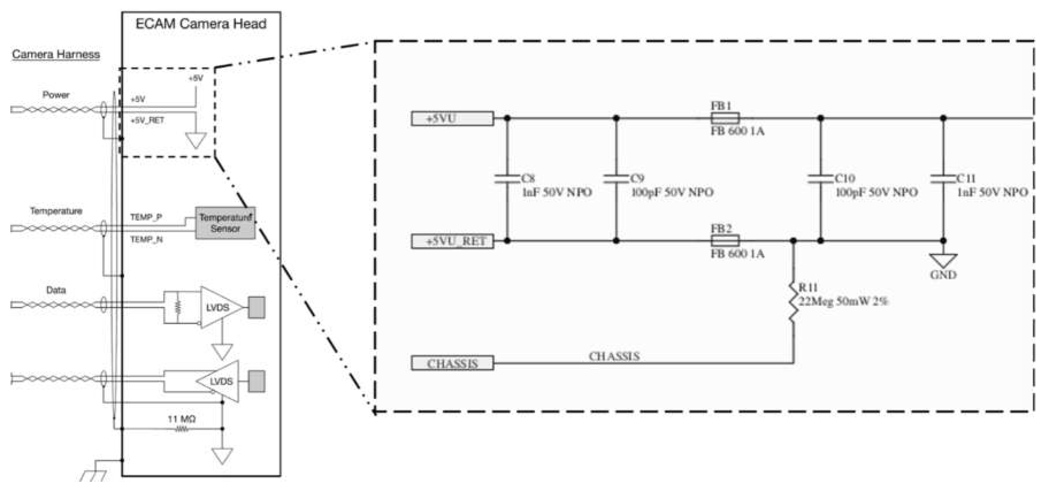
Electrical block diagram of the vision system camera head.
Figure 5.
Electrical block diagram of the vision system camera head.
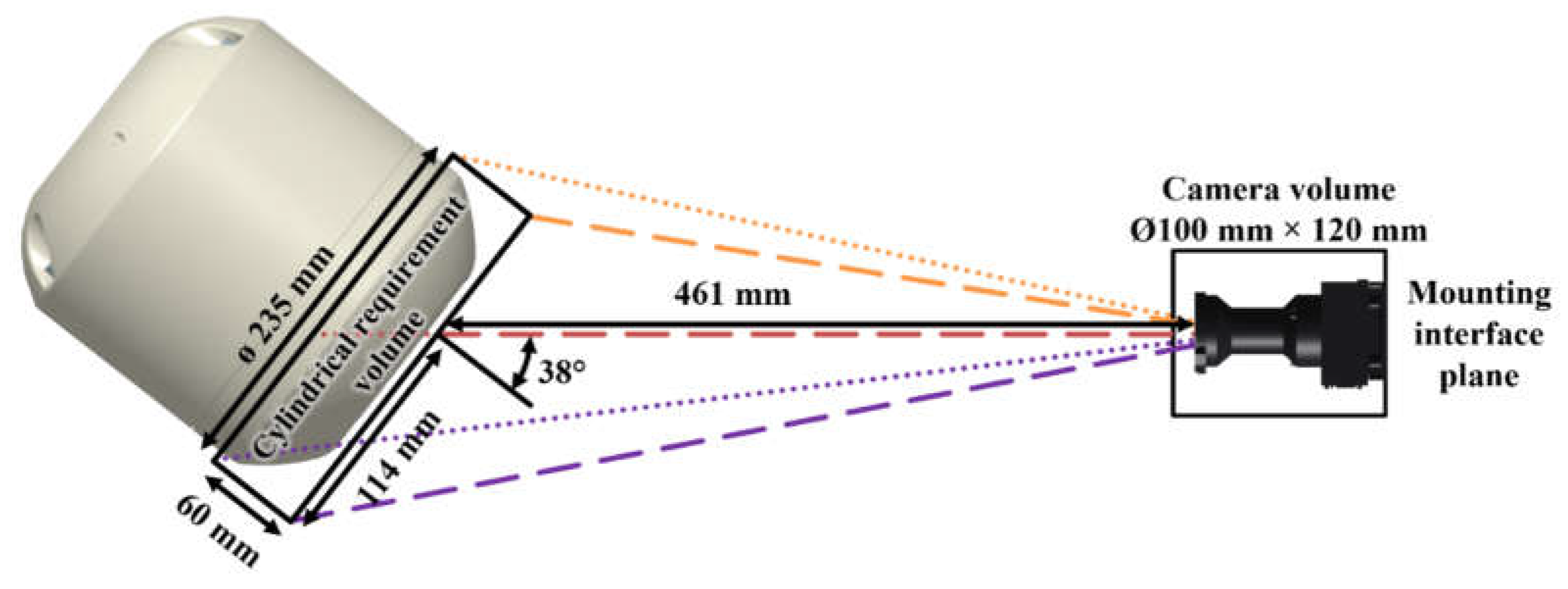
Figure 6.
Diagram of the OS depth of field volume with respect to the nominal camera locations and volume allocations. The 461 mm distance shown is from the vertex of the first lens surface to the first plane in the depth of field cylindrical volume. The best focus is set for a position 493 mm from the first lens vertex. MTF curves at the field positions illustrated above are provided in Figure 8.
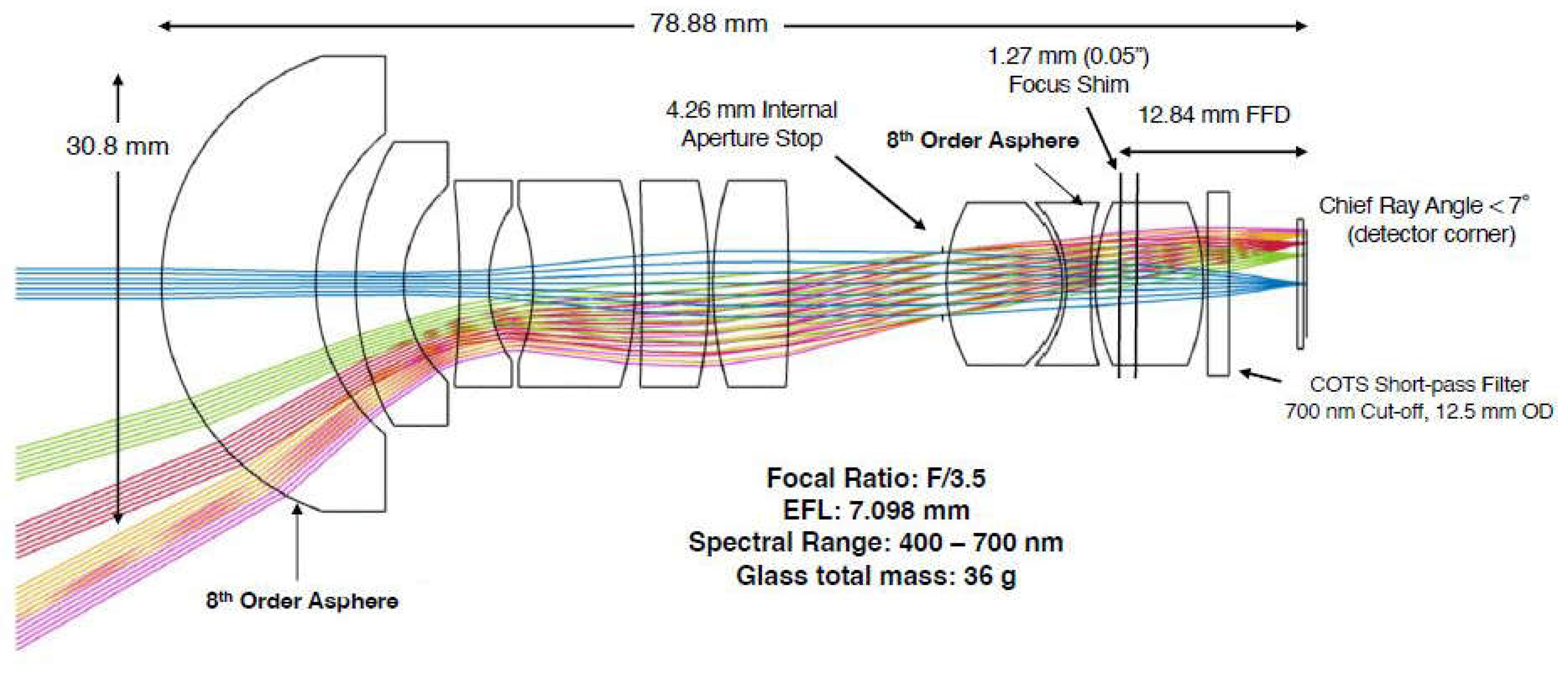
Figure 7.
Layout and ray trace of the vision system camera lens.
Figure 7.
Layout and ray trace of the vision system camera lens.
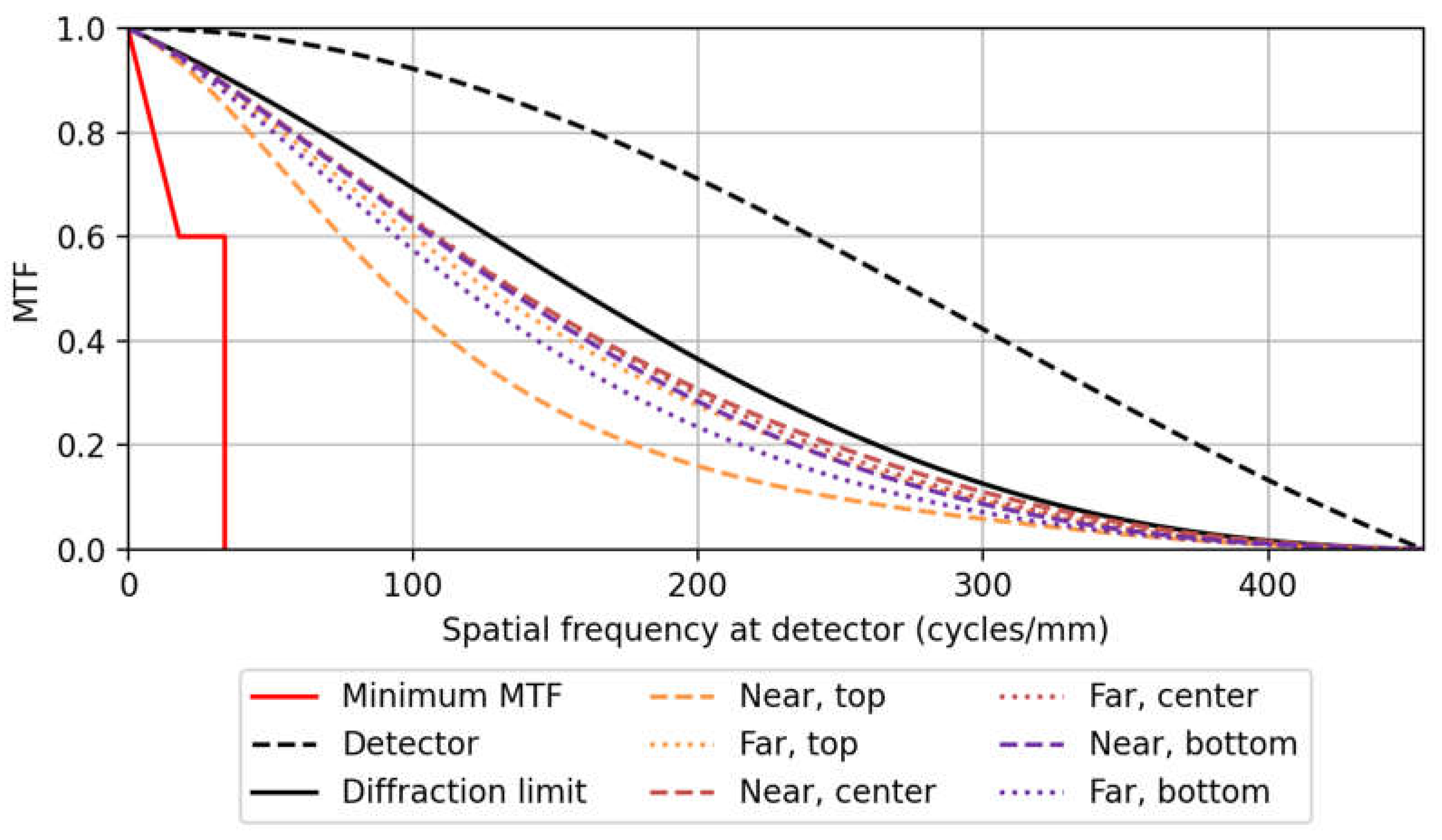
Figure 8.
The minimum required and predicted camera MTF performance at the center and corners of the camera detector active imaging area for flat planes located at the near and far planes of the depth of field requirement volume, as depicted in
Figure 6. The plot ends at a spatial frequency of 454.5 mm-1 which is equivalent to the highest sampling frequency of the detector. The prediction includes the optical as well as the detector MTF.
Figure 9.
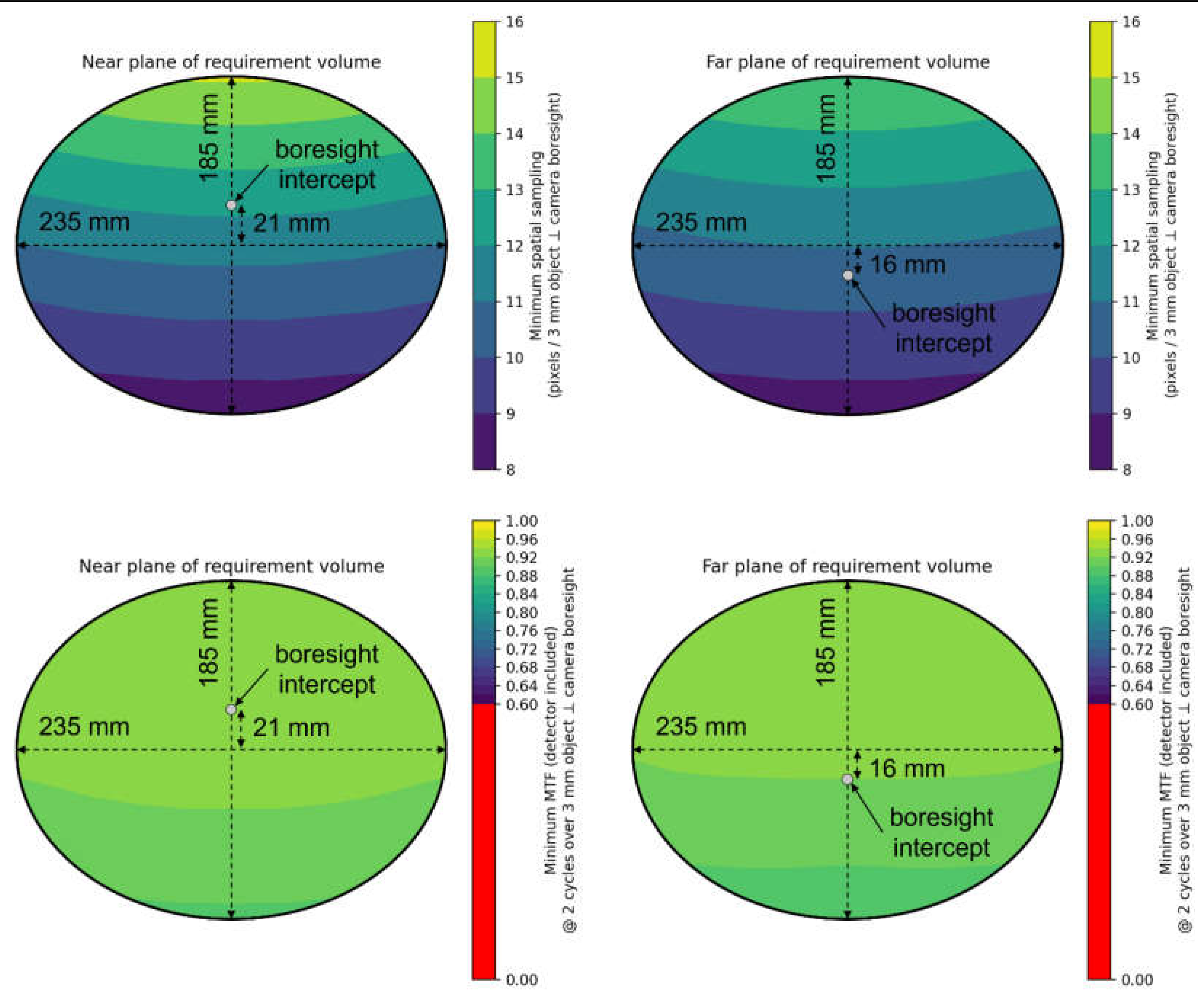
Ray trace model calculations of the detector sampling (top row) and the MTF values corresponding to two cycles across 3 mm (bottom row) at the two extreme depth of field planes for the selected vison system cameras. The calculations include optical as well as detector MTF effects. The results indicate that the cameras will have sufficient resolution and contrast to discriminate between features on the OS endcaps.
Figure 10.
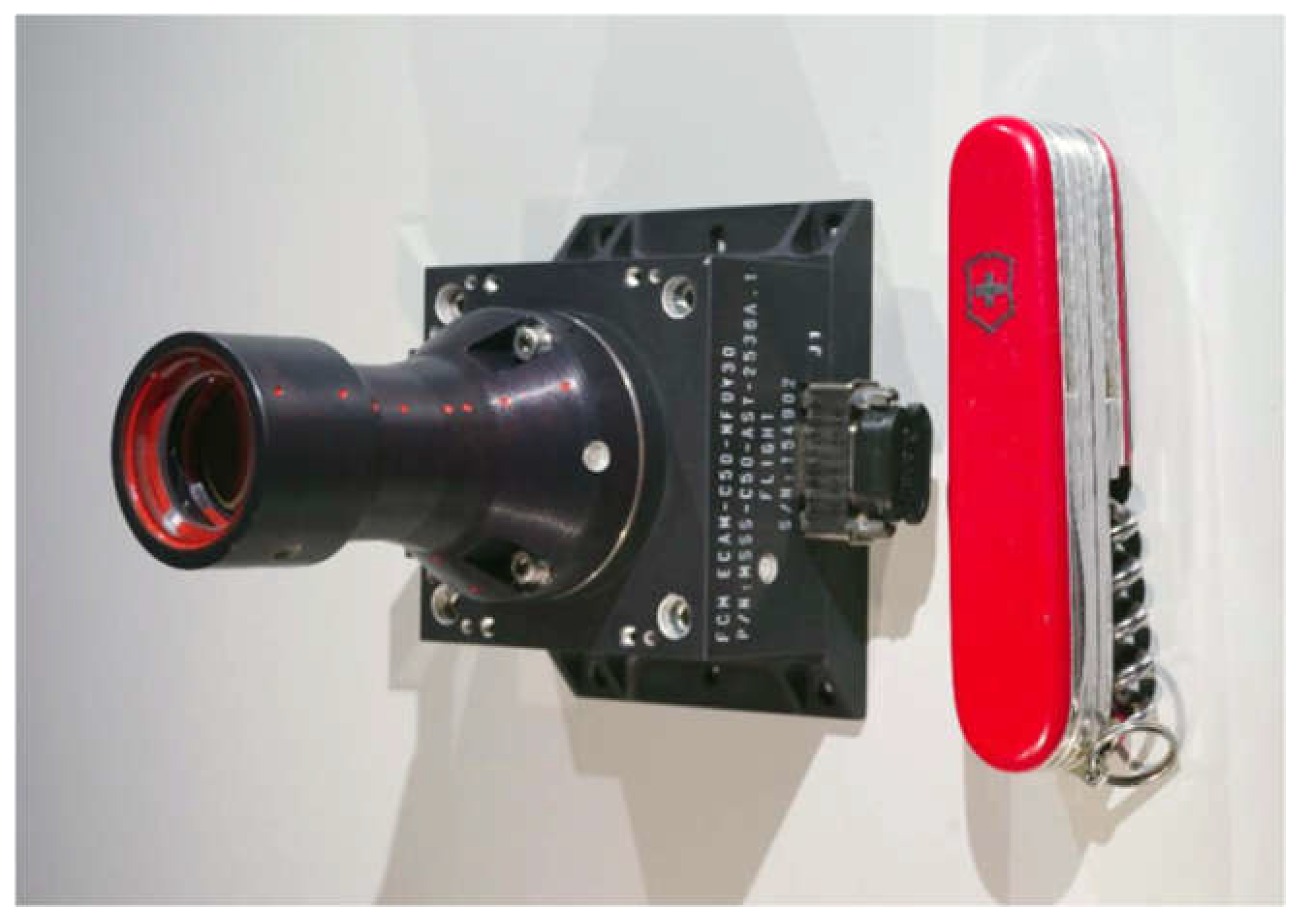
Image of a previously constructed Malin Space Science Systems (MSSS) ECAM camera that is identical to the CCRS vision system camera design.
Figure 10.
Image of a previously constructed Malin Space Science Systems (MSSS) ECAM camera that is identical to the CCRS vision system camera design.
Figure 11.
Simplified block diagram of the interface between the CCRS avionics assembly and the capture enclosure camera head. The key ground path is shown, including isolation of the camera electronics from chassis ground, which is connected to both the CCRS structure and the internal SpaceWire shields. The SpaceWire strobe signals are not explicitly shown.
Figure 12.
The Camera head ground plane connected to a +5V return through Ferrite bead and isolated from the chassis ground by 11 MΩ resistance (dual 22 MΩ resistors in parallel). Chassis grounded to the CCRS structure. Chassis connected to SpaceWire outer shield and power inner shield.
Figure 12.
The Camera head ground plane connected to a +5V return through Ferrite bead and isolated from the chassis ground by 11 MΩ resistance (dual 22 MΩ resistors in parallel). Chassis grounded to the CCRS structure. Chassis connected to SpaceWire outer shield and power inner shield.
Figure 13.
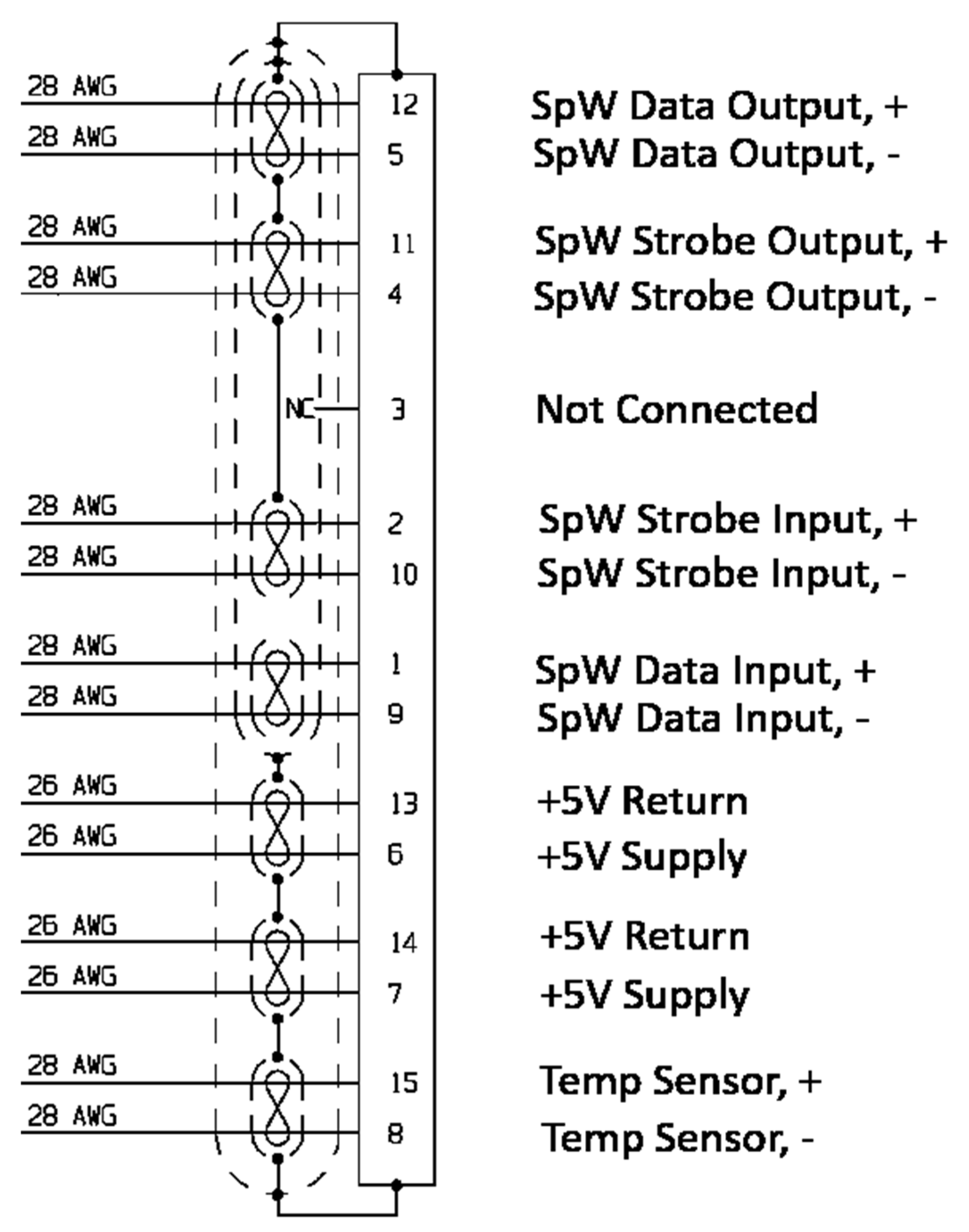
The camera 15-pin Micro-D Socket (M83513/01-BN) pinout shows chassis ground connected to the power twisted pair harness internal shields; chassis ground connected to the SpaceWire bundle shield and to strobe input and output twisted pair shields and data output twisted pair shield; data input twisted pair shield left isolated; Pin 3 not connected through harness following Spacewire Type A standard; temperature sensor also not connected through harness.
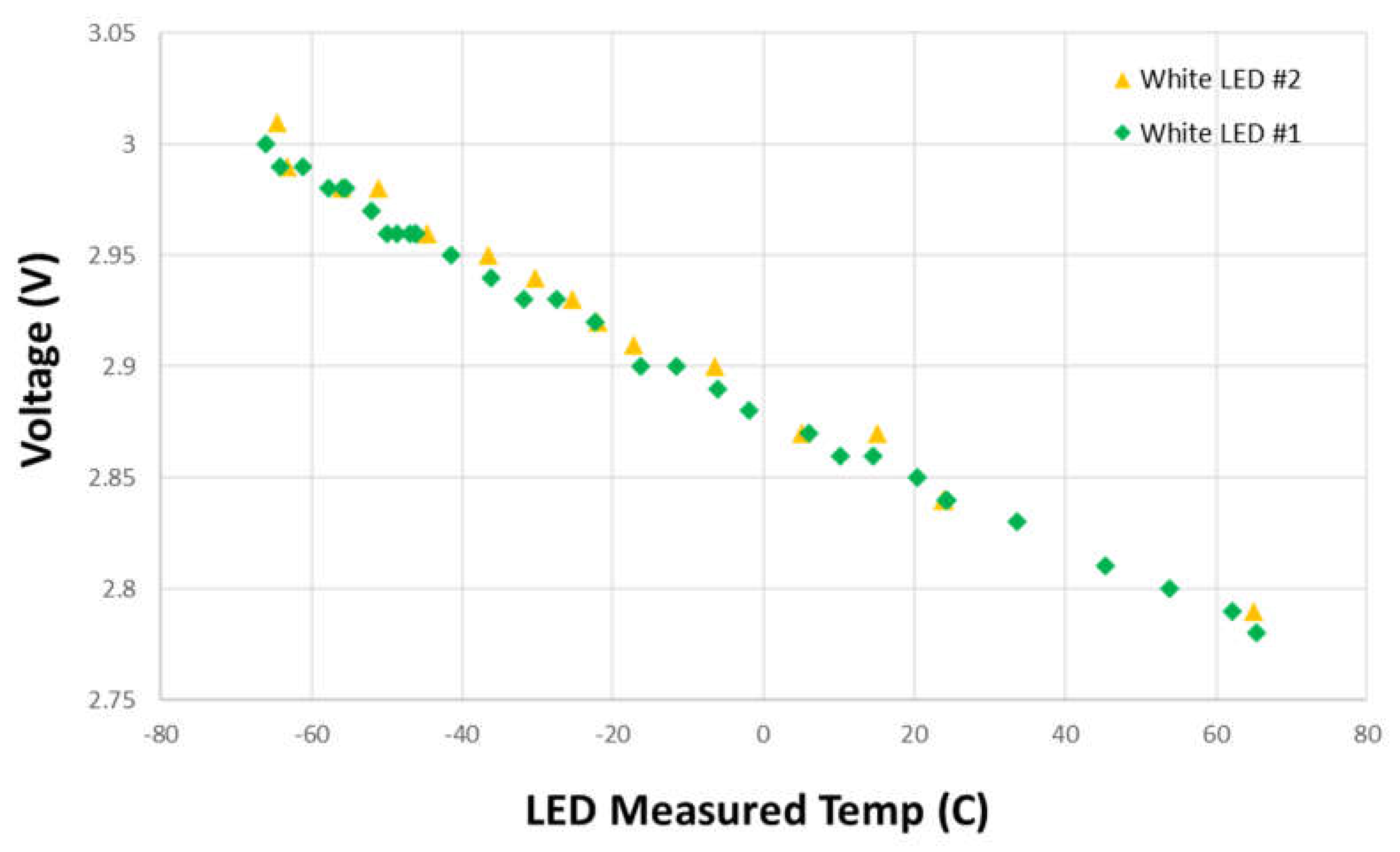
Figure 14.
LED variation of voltage with temperature from -70° C to 65° C at a constant current of 300 mA for LXZ1-4070 LED manufactured by Lumileds (San Jose, California).
Figure 14.
LED variation of voltage with temperature from -70° C to 65° C at a constant current of 300 mA for LXZ1-4070 LED manufactured by Lumileds (San Jose, California).
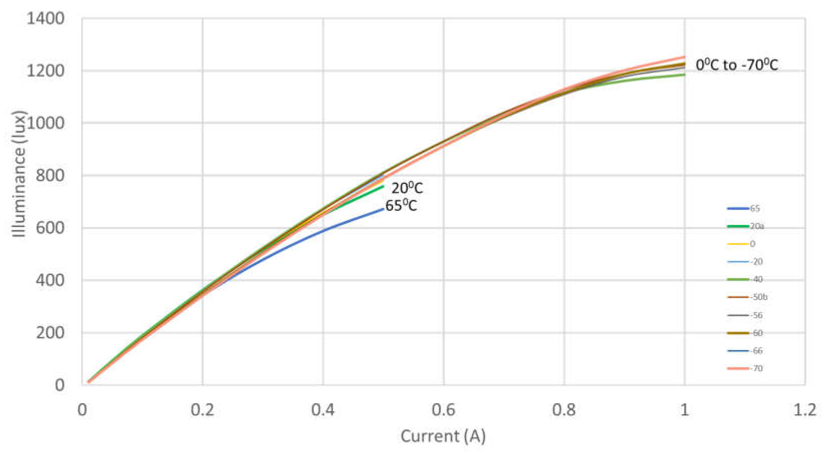
Figure 15.
Changes in LED illuminance with current sweeps ranging from 10 mA to either 500 mA or 1000 mA across a temperature range from -70° C to +65 °C.
Figure 15.
Changes in LED illuminance with current sweeps ranging from 10 mA to either 500 mA or 1000 mA across a temperature range from -70° C to +65 °C.
Figure 16.
Variation of LED light efficiency versus current at 55° C for the least efficient LED among the six LEDs tested. This represents a worst-case scenario estimation of light power, thereby providing insight into the maximum potential thermal dissipation for our illumination system.
Figure 16.
Variation of LED light efficiency versus current at 55° C for the least efficient LED among the six LEDs tested. This represents a worst-case scenario estimation of light power, thereby providing insight into the maximum potential thermal dissipation for our illumination system.
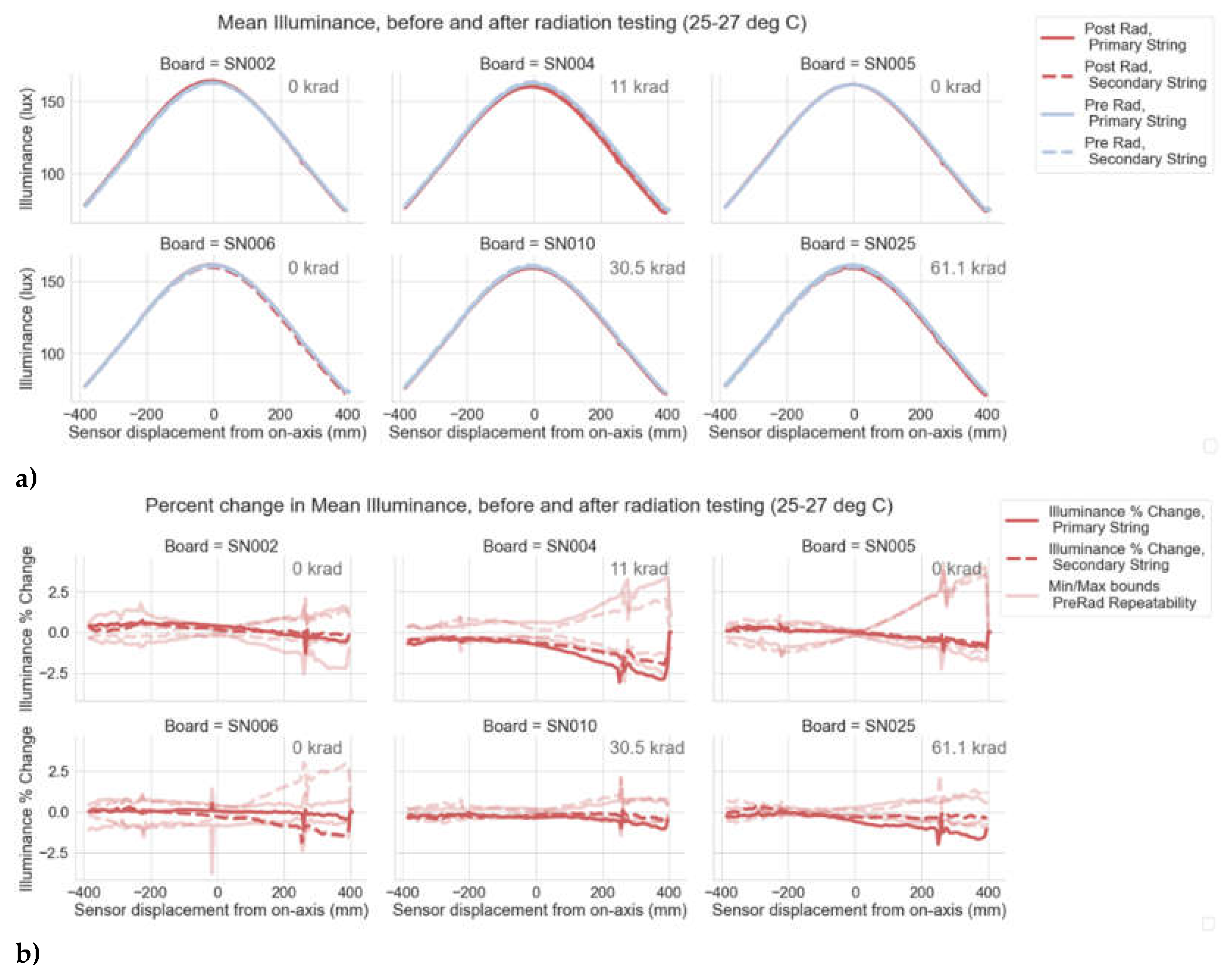
Figure 17.
Pre and post-radiation test optical characterization for LEDs exposed to various radiation dosages. No discernible changes were observed in the measured LED illumination patterns (a). The illuminance percent change data (b) indicate that optical degradation due to radiation exposure was within the measurement noise – not exceeding 3% even under the most pessimistic assumptions.
Figure 18.
Electrical diagram for a single illumination module, constructed from two independent circuits. Each circuit contains seven LEDs (LXZ1-4070) and three resistors (2010 size, 800 mW Power Rating, sourced from Vishay Intertechnology).
Figure 18.
Electrical diagram for a single illumination module, constructed from two independent circuits. Each circuit contains seven LEDs (LXZ1-4070) and three resistors (2010 size, 800 mW Power Rating, sourced from Vishay Intertechnology).
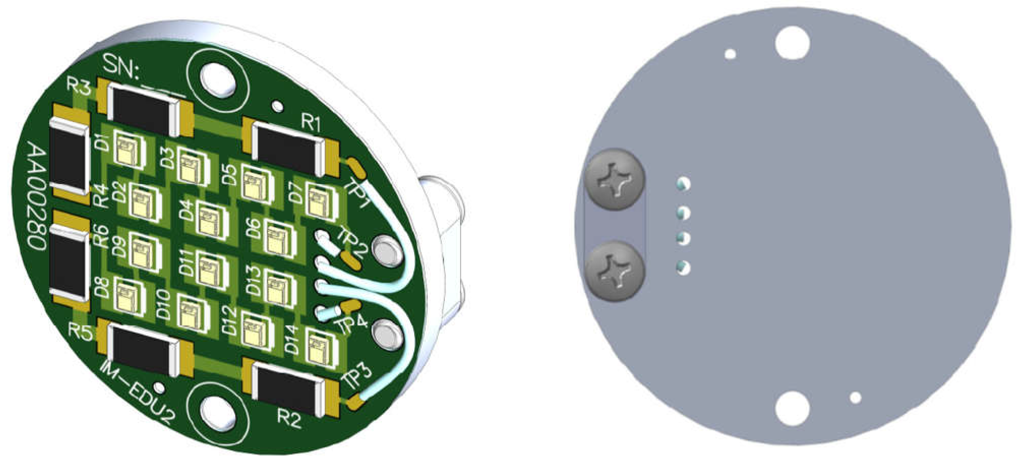
Figure 19.
Front and back surfaces of the illumination system PCB design.
Figure 19.
Front and back surfaces of the illumination system PCB design.
Figure 20.
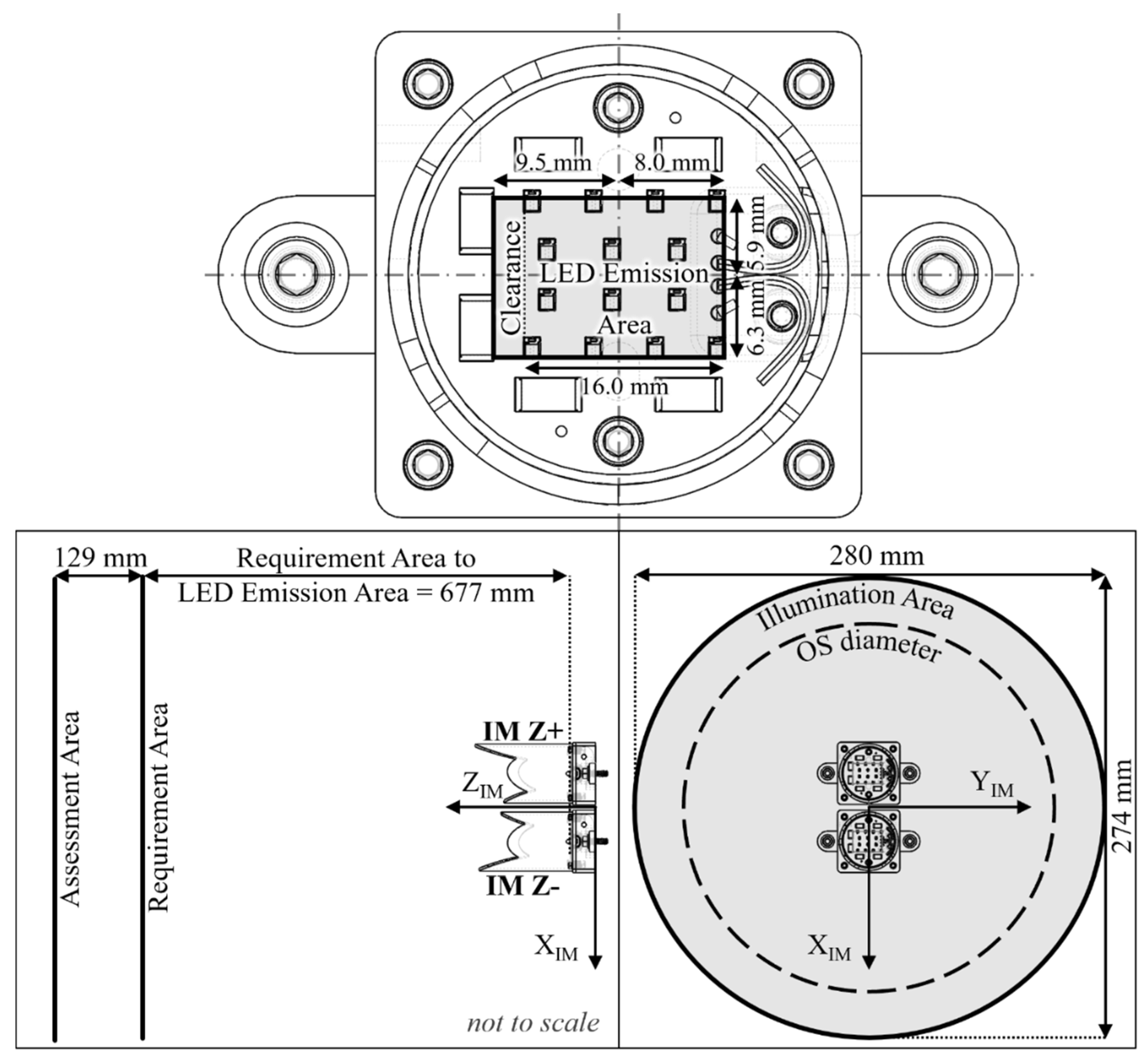
Illustration of the illumination module illumination areas over which the illuminance and uniformity requirements are to be met to ensure visibility of the OS endcaps (bottom). The illumination module baffle was designed using the near requirement area (located 677 mm away from the LED emission area) due to its being the most constraining. An oversized rectangle surrounding the 14 LEDs was used to represent the LED emission area in the design. Additional clearance to the LED emission area was added to one side of the rectangle to eliminate mechanical interference between one of the illumination modules’ baffle petals and the CCRS capture cone.
Figure 21.
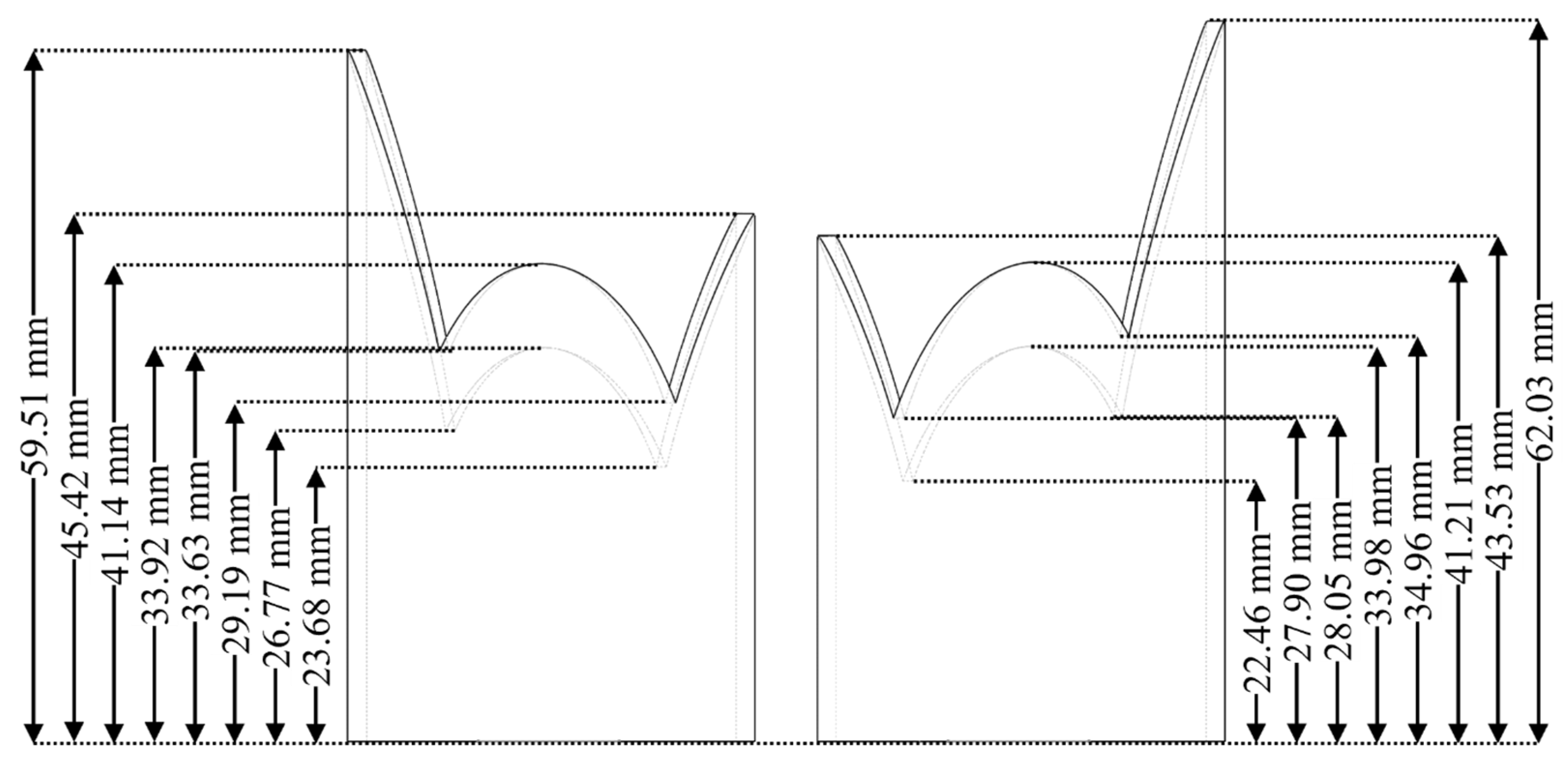
Illumination module baffle designs for the -Z (left) and +Z (right) illumination modules that maximize the light uniformity in the required illumination areas but minimize the light that strikes other areas. Dimensions indicate the distances between the LED emission plane and the baffle aperture minima and maxima dimensions.
Figure 22.
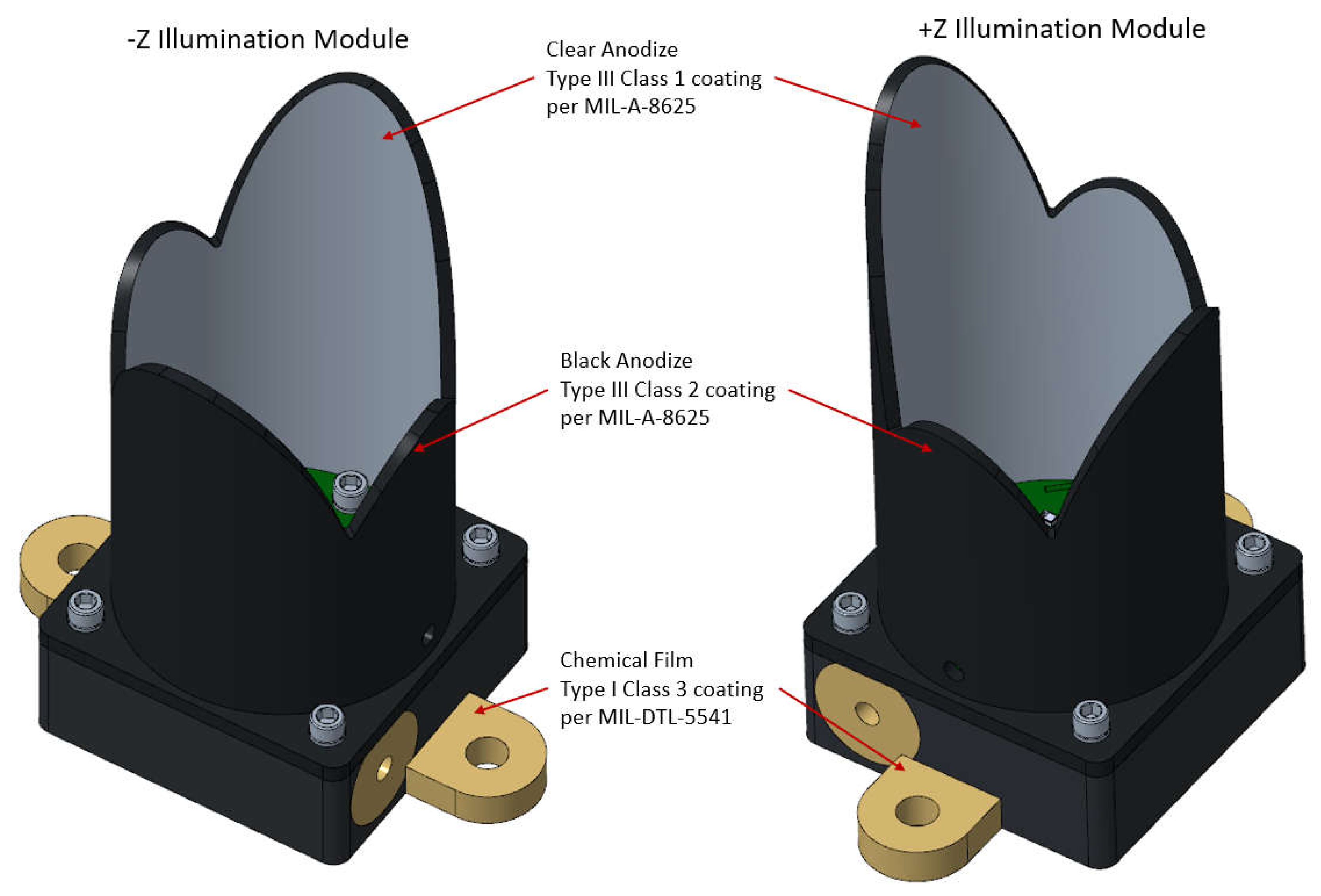
Mechanical design with coating specifications, showing two unique baffle designs and one common base design for each module.
Figure 22.
Mechanical design with coating specifications, showing two unique baffle designs and one common base design for each module.
Figure 23.
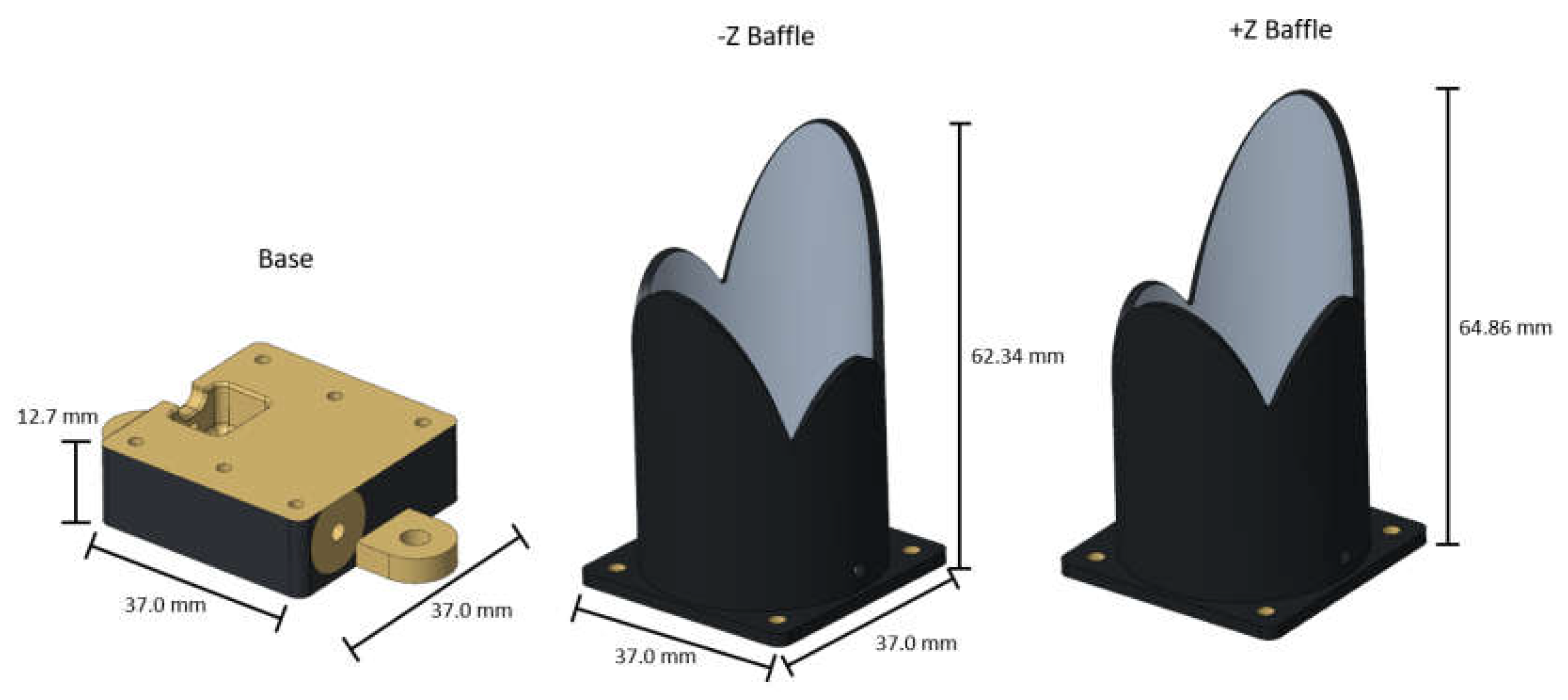
Overall dimensions of the illumination modules.
Figure 23.
Overall dimensions of the illumination modules.
Figure 24.
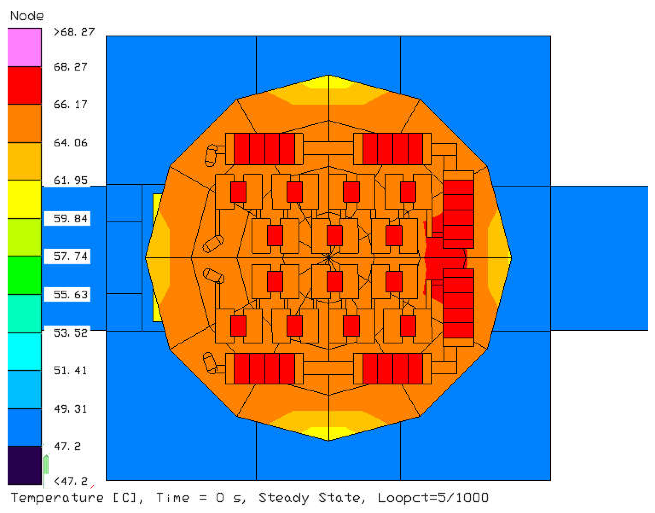
Thermal model simulation results showing the LED junction and resistor temperatures meet the component specifications with margin.
Figure 24.
Thermal model simulation results showing the LED junction and resistor temperatures meet the component specifications with margin.
Figure 25.
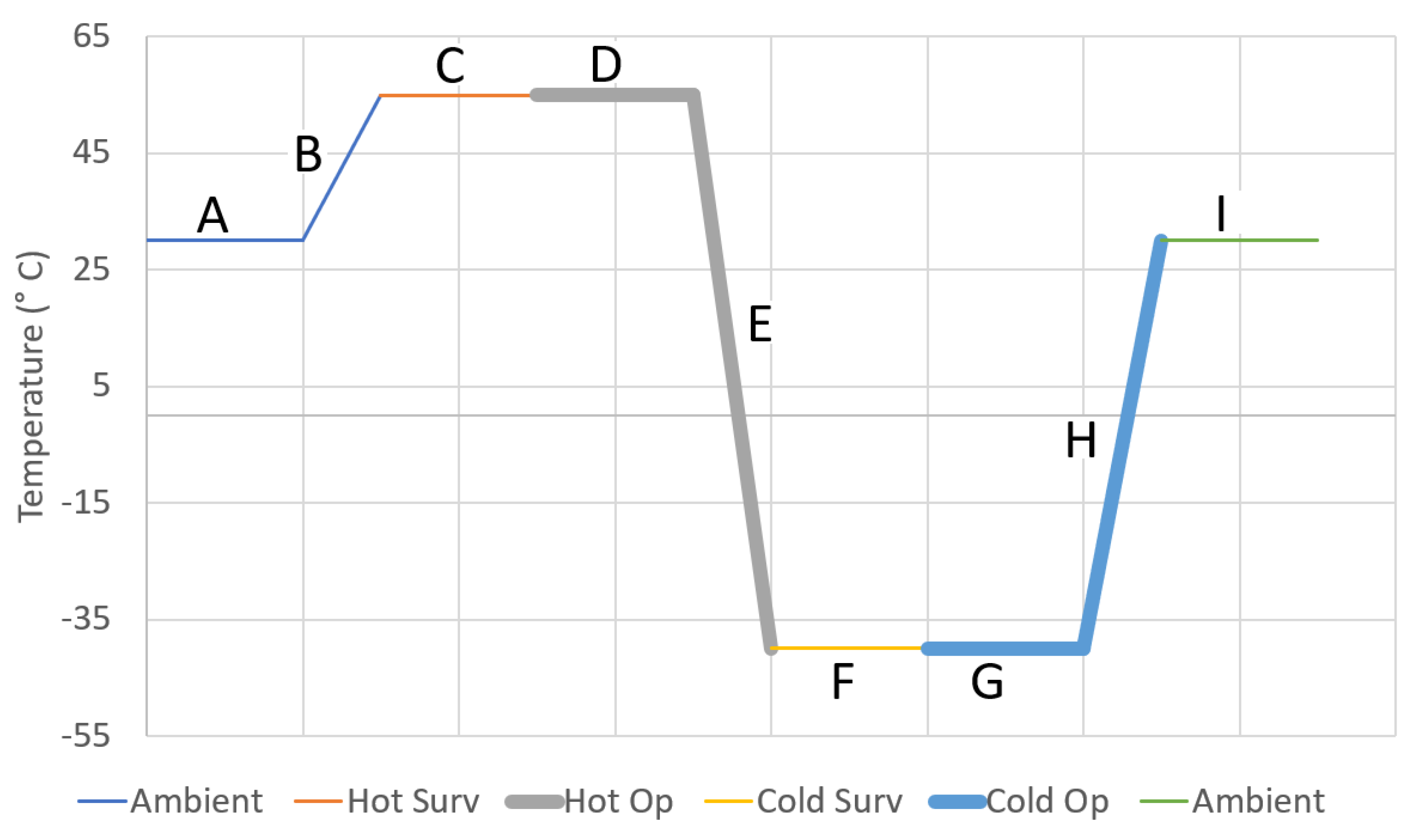
Graphical representation of the EDU illumination module thermal vacuum test temperature profile.
Figure 25.
Graphical representation of the EDU illumination module thermal vacuum test temperature profile.
Figure 26.
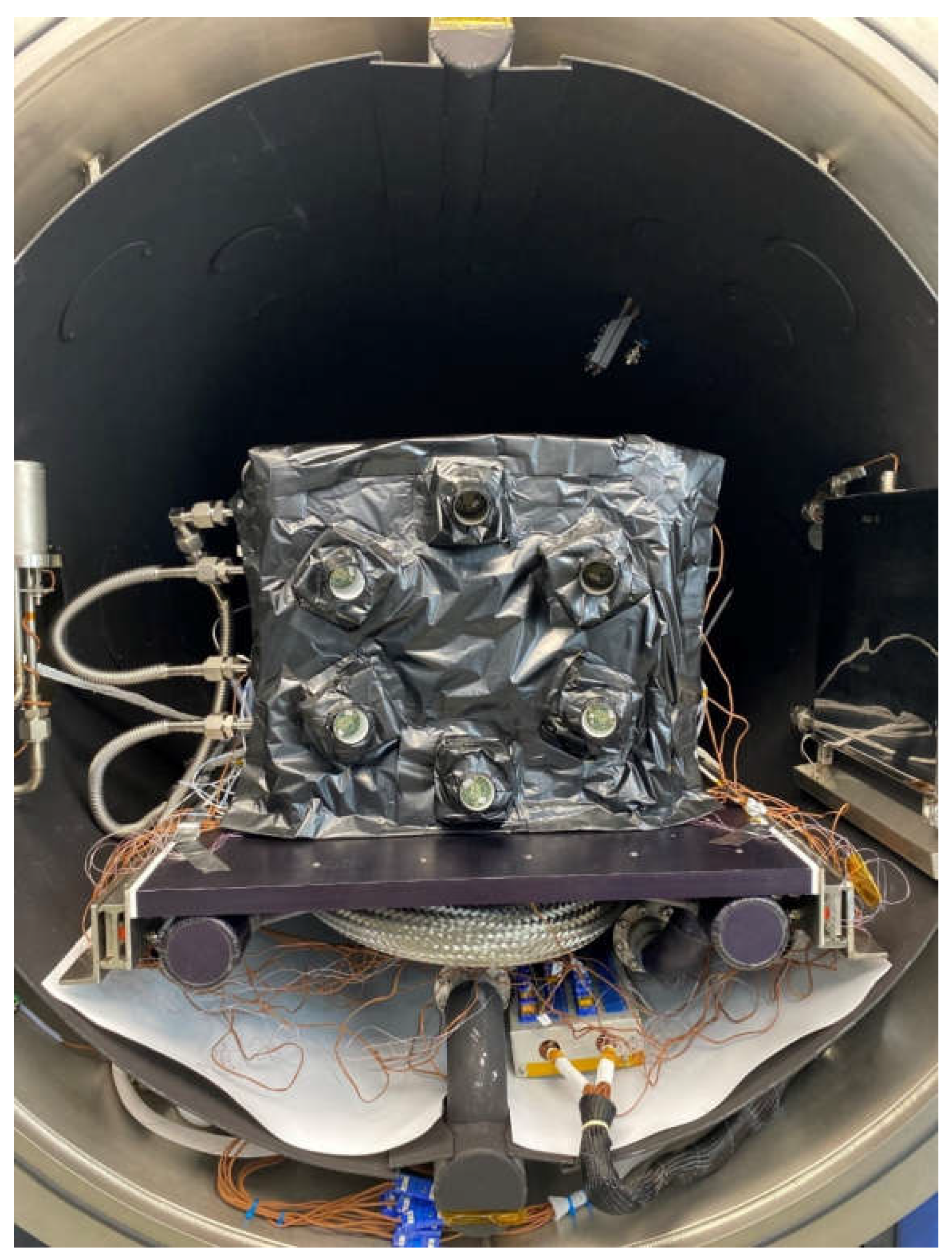
EDU illumination module thermal vacuum test set-up prior to chamber door closure. Six test articles are visible with views of the PCBs looking along the baffle interiors.
Figure 26.
EDU illumination module thermal vacuum test set-up prior to chamber door closure. Six test articles are visible with views of the PCBs looking along the baffle interiors.
Figure 27.
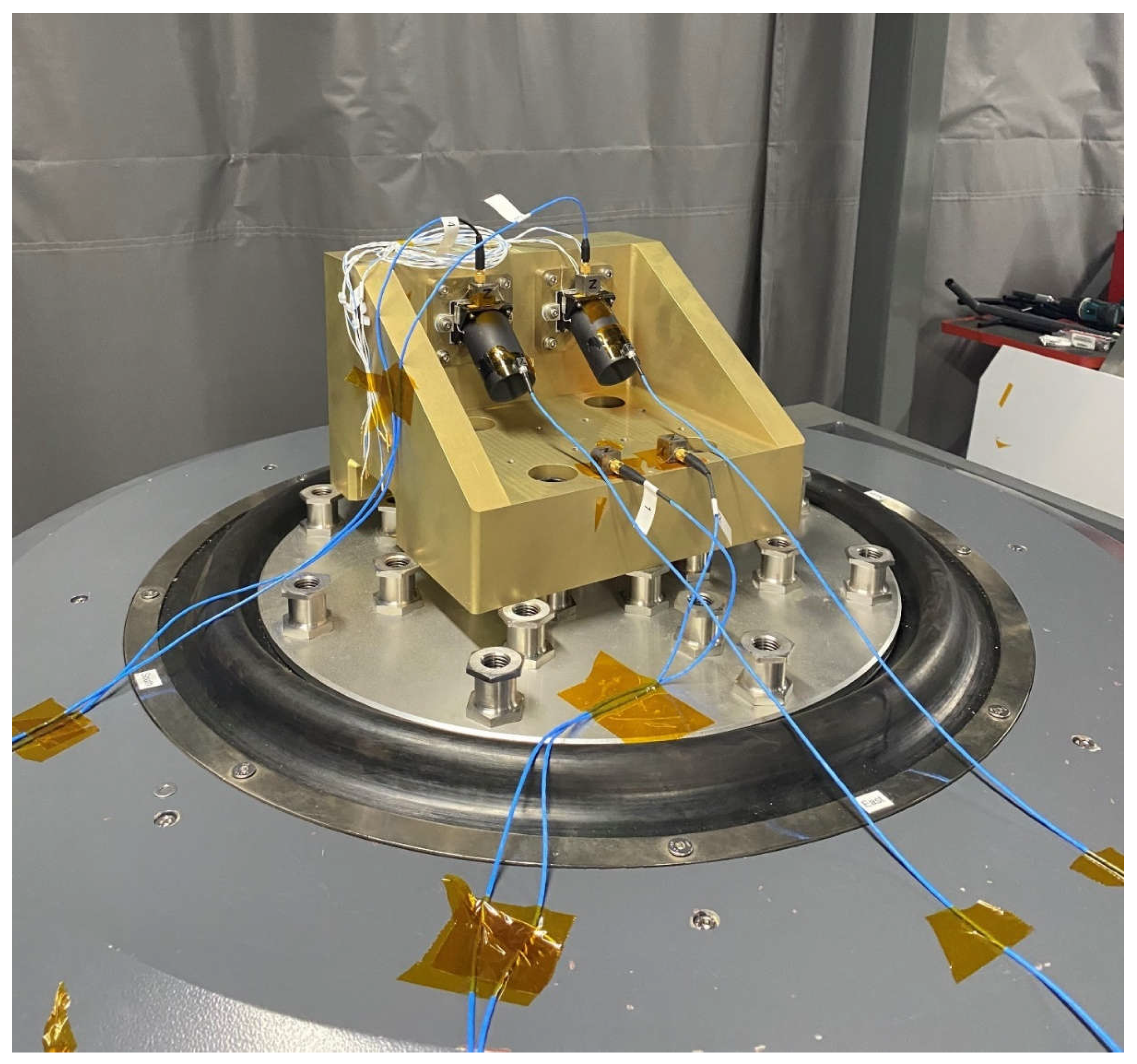
EDU illumination module vibration test arrangement. This set up allowed two illumination modules to be tested at the same time.
Figure 27.
EDU illumination module vibration test arrangement. This set up allowed two illumination modules to be tested at the same time.
Figure 28.
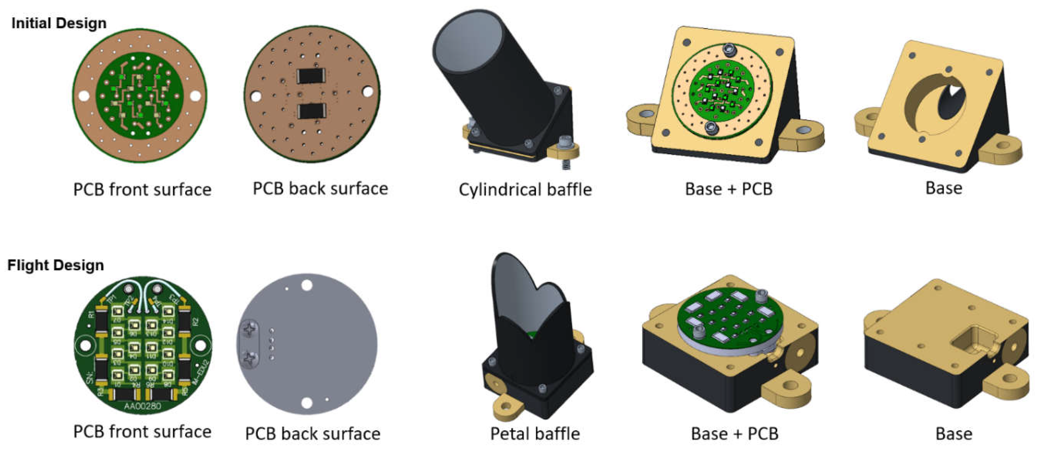
Illustration of the changes made to the initial illumination module design based on the lessons learned from the EDU fabrication and test activities.
Figure 28.
Illustration of the changes made to the initial illumination module design based on the lessons learned from the EDU fabrication and test activities.
Figure 29.
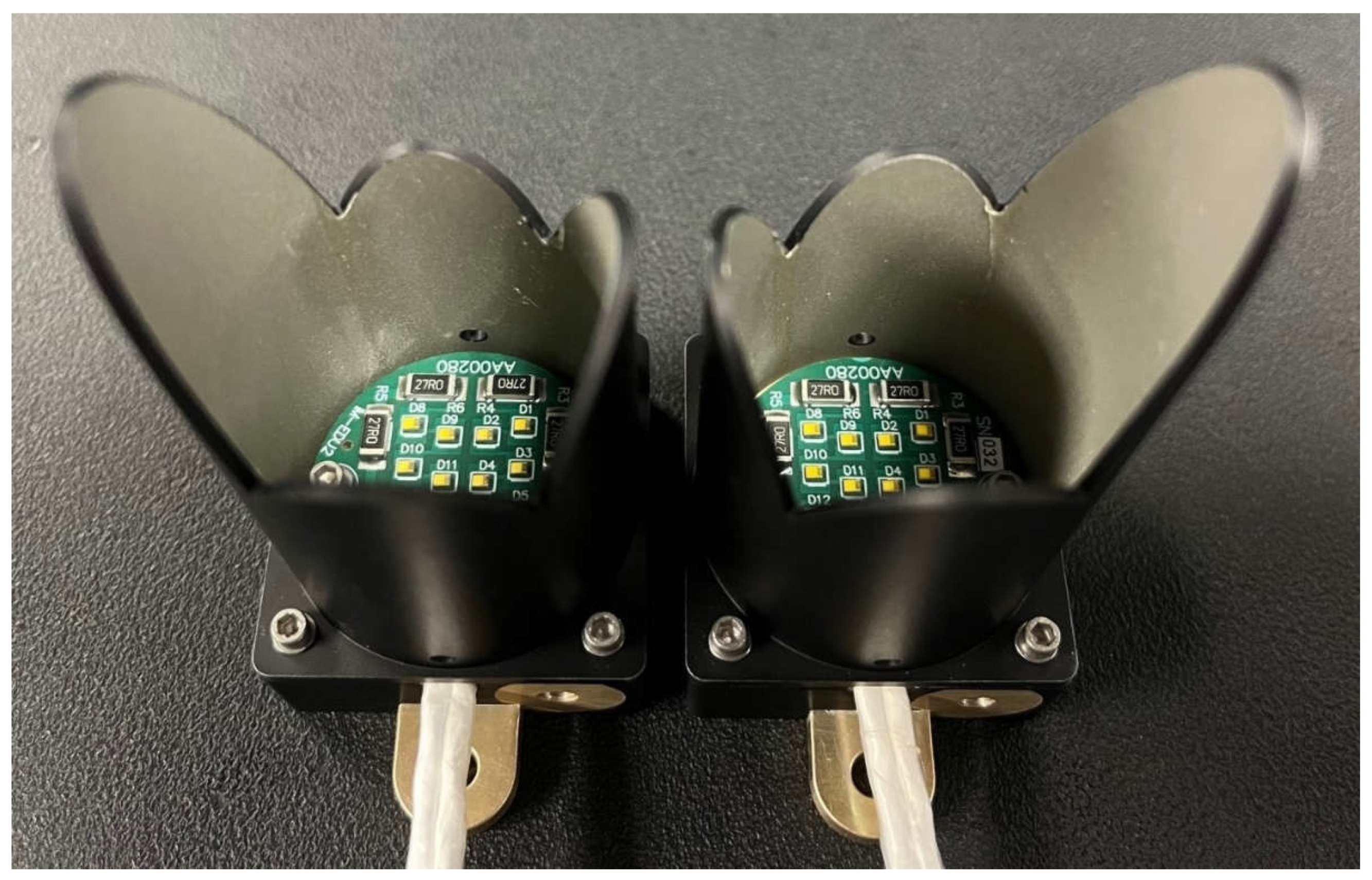
Image of two of the EDU illumination modules constructed from the flight model design. Although the -Z module (left) and the +Z module (right) baffles appear to be mirror copies they are not exact mirror-matches due to the use of a common module base. The small hole visible near the PCB in each module is for EDU test instrumentation and will not be present in the flight models (Photo Credit: Katherine M. Mellos).
Figure 30.
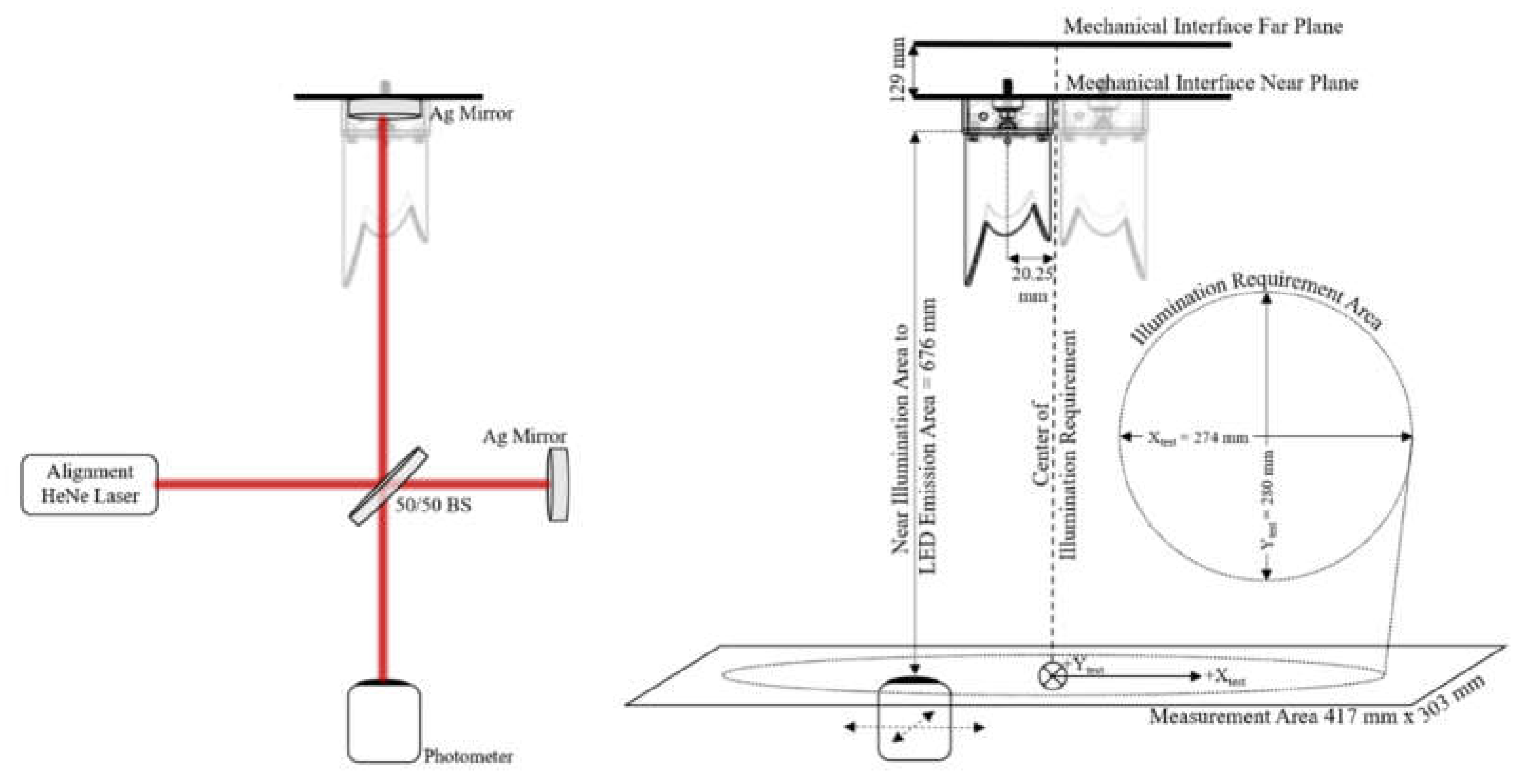
Illustration of the EDU illumination module optical test set-up. The diagram on the left shows the alignment approach used to minimize the tip/tilt between the illumination module LED emission plane surface normal and the optical measurement plane. The diagram on the right shows the optical test dimensions. Note the test distance is 1 mm different from the distance originally used to design the baffle due to late changes in the illumination module design and CCRS accommodations.
Figure 31.
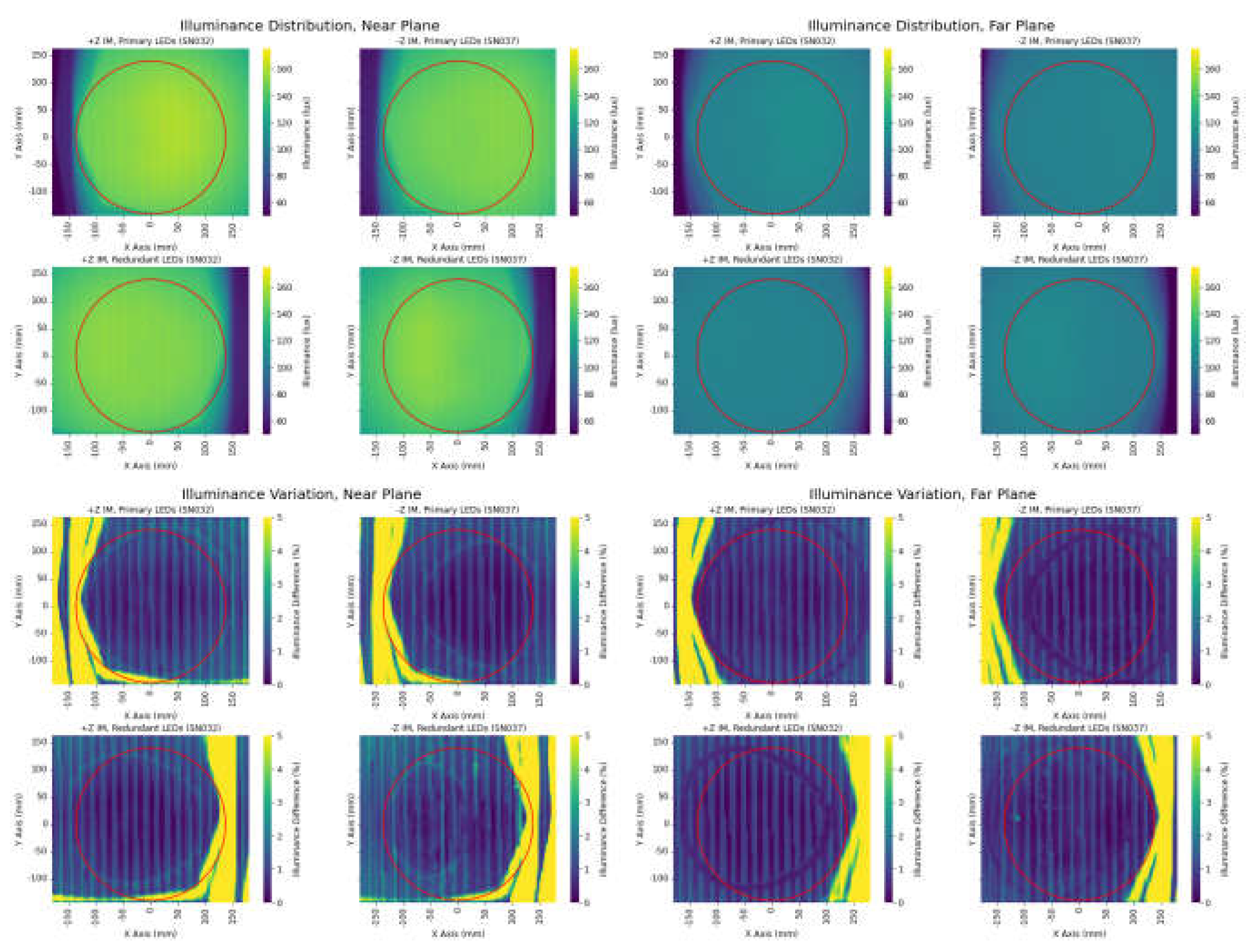
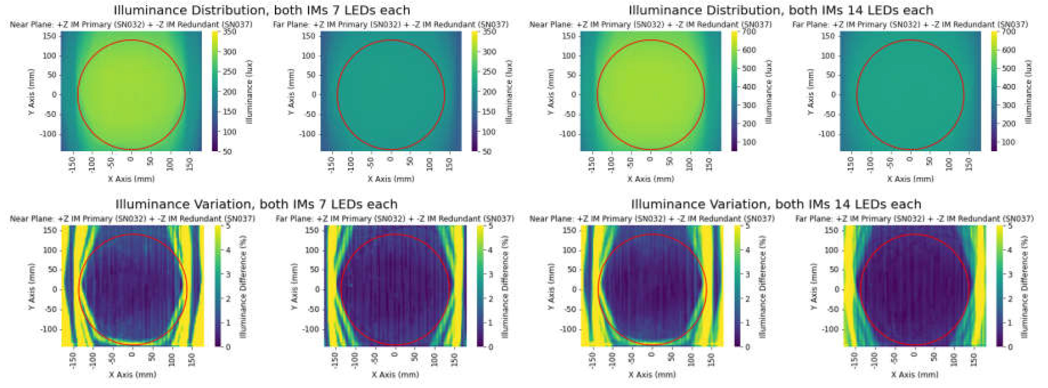
EDU illumination module optical test results at both the near (left) and far (right) evaluation planes for the two +Z illumination modules and two -Z illumination modules. In all eight cases the maximum and minimum illuminance requirements are met over the required area (red circle). The illuminance variation requirement is also met over most of the required area (red circle) for all eight EDU modules except for areas ~5 mm x 12 mm in size near the edge of the requirement zone where the variation is 5% or more. A subsequent investigation has found that this non-compliance was mistakenly designed into the baffles due to a misunderstanding of the SolidWorks “Lofted Cut” feature. Note that the low-level periodic variation running left to right in the illuminance uniformity results are not present in the optical patterns but are caused by periodic noise in the photometer.
Figure 32.
EDU illuminance results over the required area (red circle) when the primary 7 LEDs in each illumination module are powered on (left) and all 14 LEDs in each illumination module are powered on (right). With 7 LEDs in each illumination module powered on the illuminance doubles when compared to only one module being powered on (see
Figure 31). With 14 LEDs in each illumination module powered on the illuminance doubles when compared to 7 LEDs being powered in each illumination module. For the case with all LEDs powered on the small areas at the near plane where the illuminance uniformity is >5% appear on both sides of the required area while the individual areas of non-uniformity shrink. Although the nominal vision system operations concept assumes only 7 LEDs in each illumination module are powered on, for operational efficiency the CCRS operations concept currently assumes all LEDs (28) will be powered on during imaging.
Figure 33.
BRDF measurements of CCRS surface treatments relevant to the vision system at 440 nm (left column), 550 nm (middle column) and 700 nm (right column) for (a) Ceranovis pre-friction test, (b) Ceranovis post-friction test, (c) aluminum 6061 with Teflon coating and (d) aluminum 7075 with Teflon coating.
Figure 34.
Vison system surface treatment BRDF measurements of (a) 3D printed material at 440 nm (left), 550 nm (center) and 700 nm (right) for the OS endcap surrogates, (b) 550 nm measurements of bead-blasted aluminum with clear anodize at 20 psi (left), 30 psi (center) and 40 psi (right), (c) 30 psi bead-blasted aluminum with clear anodize at 440 nm (left), 550 nm (center) and 700 nm (right) and (d) black anodized aluminum at 440 nm (left), 550 nm (center) and 700 nm (right).
Figure 35.
Vision system laboratory testbed utilizing commercially available off-the-shelf (COTS) cameras, engineering development unit (EDU) illumination modules and 3D-printed representations of the CCRS capture cone, orientation mechanism and both OS container endcaps (Photo Credit: Katherine M. Mellos).
Figure 36.
MTF of the lab testbed lens (orange), the flight camera lens (blue) and the minimum allowable vision system camera optics (red).
Figure 36.
MTF of the lab testbed lens (orange), the flight camera lens (blue) and the minimum allowable vision system camera optics (red).
Figure 37.
BRDF comparison for a variety of incidence angles (AOI) of the two laboratory testbed OS surface finishes (3D resin and 3D metallic paint) to the two OS surface finishes (CN145 Li-Doped and Req. limit) used in the non-sequential ray trace model. The 3D resin (a) represents the current OS surface finish in the testbed and matches well to the Ceranovis BRDF modeled in the non-sequential model except for the specular peak caused by friction testing. The metallic paint (b) represents the worst-case OS surface finish currently allowed by OS requirements. It agrees well with the OS BRDF requirement limit, particularly near the specular peaks.
Figure 38.
System level images from the -Z camera position in the laboratory testbed, showing the vision system baseline performance for the lab surrogate of the current OS surface finish. Right column shows same images reporting calibrated luminance values. Red indicates the areas in the image below the 7.8 candela/m2 OS luminance requirement. No areas on the OS are below the luminance requirement.
Figure 39.
System level images from the -Z camera position laboratory testbed, showing the baseline vision system performance for an OS with the most specularly reflective surface finish allowed by requirements. Right column shows same images reporting calibrated luminance values. Red indicates the areas in the image below the 7.8 candela/m2 OS luminance requirement. Except for a few small points, the majority of the OS surface meets the luminance requirement.
Figure 40.
FRED BRDF model fit at various angles of incidence (AOI) to the measured data for the Ceranovis-145 with Li-Doped sealant after going through surface friction testing.
Figure 40.
FRED BRDF model fit at various angles of incidence (AOI) to the measured data for the Ceranovis-145 with Li-Doped sealant after going through surface friction testing.
Figure 41.
View of the CCRS vision system non-sequential ray trace model components. It includes: both cameras, both illumination modules, the capture cone with porthole strengthening members, the major portions of the orientation mechanism and the OS.
Figure 41.
View of the CCRS vision system non-sequential ray trace model components. It includes: both cameras, both illumination modules, the capture cone with porthole strengthening members, the major portions of the orientation mechanism and the OS.
Figure 42.
View of the CCRS vision system non-sequential ray trace model components looking from the capture side along the CCRS Y-axis. Viewable items include: both cameras, both illumination modules, the capture cone interior, one OS endcap and small portions of the orientation mechanism.
Figure 42.
View of the CCRS vision system non-sequential ray trace model components looking from the capture side along the CCRS Y-axis. Viewable items include: both cameras, both illumination modules, the capture cone interior, one OS endcap and small portions of the orientation mechanism.
Figure 43.
Comparison of the OS base luminance results from the laboratory measurements and the FRED non-sequential ray trace model prediction. Agreement between the two results is typically ~10%, consistent with our photometer calibration uncertainty and our ability to measure and model the OS BRDF. Luminance values shown in the table above are region averages calculated within square windows equivalent to a 28x28 pixel area on the flight vision system camera detector.
Figure 44.
Four nominal vision system imaging performance predictions for the OS lid (top row) and OS base (bottom row) based on the laboratory testbed results for the +Z camera (left column) and -Z camera (right column) with the primary LED circuits in both illumination modules providing illumination.
Figure 45.
Eight nominal vision system performance predictions for the OS lid (top row) and OS base (bottom row) based on non-sequential ray trace modeling in FRED. Left to right: +Z camera, primary circuit LEDs; +Z camera, redundant circuit LEDs; -Z camera, primary circuit LEDs; -Z camera, redundant circuit LEDs.
Figure 46.
Eight worst-case vision system performance predictions for the OS lid (top row) and OS base (bottom row) based on non-sequential ray trace modeling in FRED. The worst-case lens contamination; OS surface treatment; OS position and orientation; lens performance and detector noise are added to the nominal conditions to create the images. Left to right: +Z camera, primary circuit LEDs; +Z camera, redundant circuit LEDs; -Z camera, primary circuit LEDs; -Z camera, redundant circuit LEDs.
Figure 47.
Four nominal vision system performance predictions for the OS lid (top row) and OS base (bottom row) based on non-sequential ray trace modeling in FRED when all 28 vision system LEDs are powered on. +Z camera images are shown in the left column. -Z camera images are shown in the right column.
Figure 48.
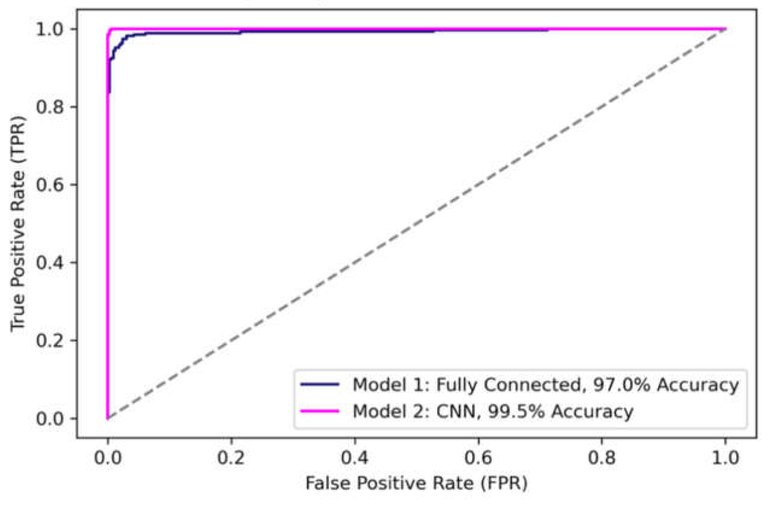
The receiver operating characteristic (ROC) curves for the trained fully connected network (FCN) and convolutional neural network (CNN) models, which illustrates the false positive rate at different decision thresholds. ROC curves that stay close to the top left corner indicate better performance while the dashed line corresponds to random (50/50) classification.
Figure 49.
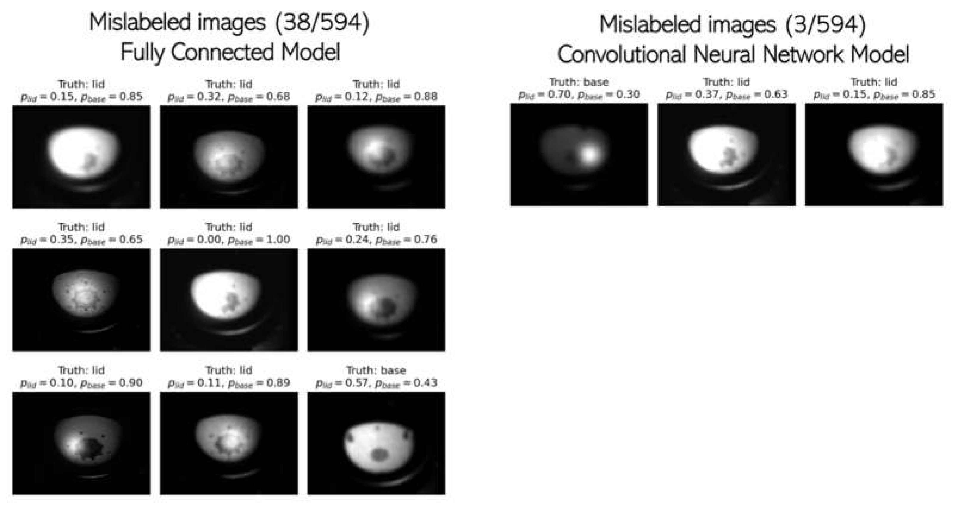
Examples of misidentified images and the corresponding probabilities calculated by each neural network model for a decision (identification) threshold set to p > 0.5. Left: A random sample of nine test images from the 38 that were misidentified by the FCN model. Several images that are easily identified by humans are confidently given the incorrect label by the model; for example, the bottom middle image is identified as a base endcap with an 89% probability. Right: The three test images that were misidentified by the CNN model. These would also be challenging for a human observer to identify.
Figure 50.
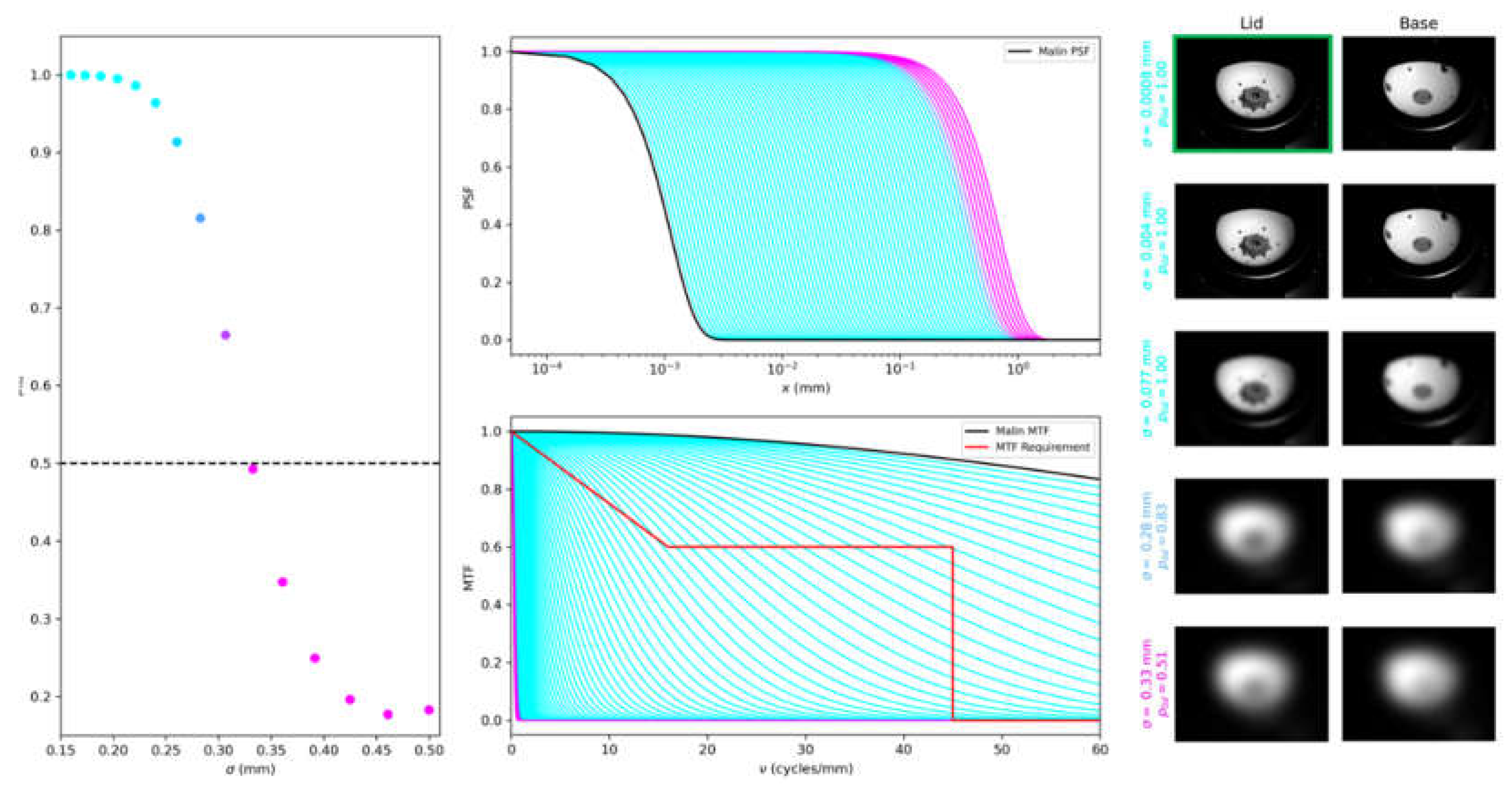
The impact of increasing Gaussian blur widths on the confidence of the CNN model. Different levels of blurring were applied to an image of the lid endcap, which is outlined in green on the rightmost panel. All units are in image space. Left: Probabilities generated by the CNN for different Gaussian convolution kernel widths. Images that fall below the decision threshold of 0.5 are colored pink. Bluer points correspond to a higher confidence in identification. Middle top: The Gaussian convolution kernels, which are effectively PSFs, next to the expected PSF of the vision system cameras (labeled “Malin PSF”). The curves are color-coded to match the points—or probabilities—shown to the left. Middle bottom: The MTF for each of the blurring cases, which are the modulus of the Fourier transform of the PSFs. Right: Five levels of blurring applied to the images of the lid and the base. The top row corresponds to the nominal vision system camera PSF.
Figure 51.
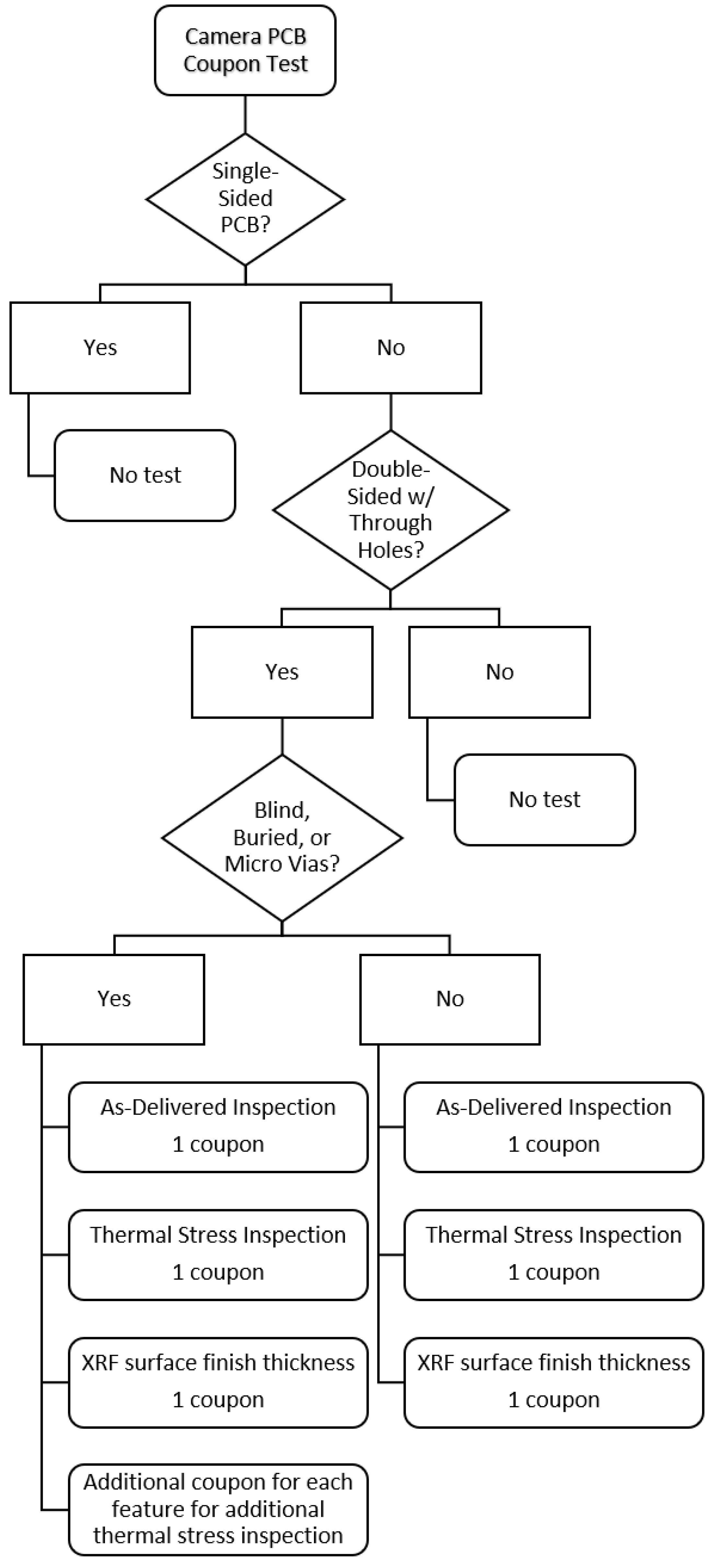
Summary of the vision system camera PCB pre-population inspection process.
Figure 51.
Summary of the vision system camera PCB pre-population inspection process.
Figure 52.
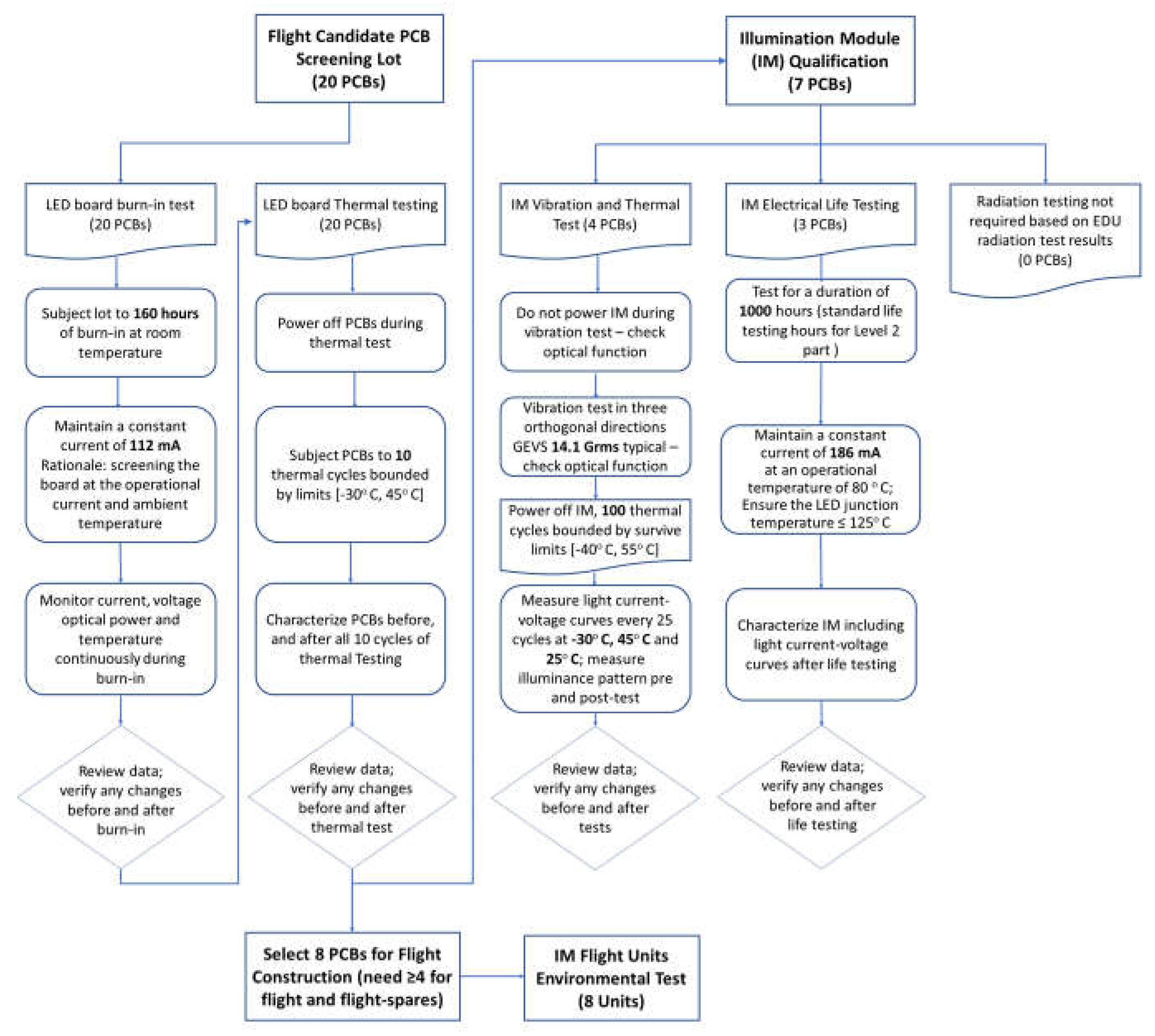
Summary flow diagram of the illumination system printed circuit board (PCB) flight screening and illumination module qualification plans.
Figure 52.
Summary flow diagram of the illumination system printed circuit board (PCB) flight screening and illumination module qualification plans.
Table 1.
Summary of the key CCRS-to-vision system interface values. Values in brackets represent the maximum allowed while other values shown are the current best estimate (CBE).
Table 1.
Summary of the key CCRS-to-vision system interface values. Values in brackets represent the maximum allowed while other values shown are the current best estimate (CBE).
| Key CCRS Vision System Interface Values – CBE [Max Budget] |
|---|
| Metric |
Camera (each) |
Illumination Module (each) |
| Mass (kg) |
0.5 [0.525]
without cable |
0.075 [0.115]
without flying leads |
| Volume (mm) |
100 (dia) by 120 (height) |
Base 62x38 x 18(height)
Baffle Ø36 x 36(height) |
| Distance (mm) mounting plane to OS endcap |
589.44 |
723.56 |
| Angle (deg) boresight to OS centerline |
38.0 |
26.5 |
| Data Interface |
SpaceWire |
N/A |
| Power (W) |
2.0 [2.5] |
6.35 [7.0] |
| Supplied Bus Voltage (V) |
5 (unswitched) |
28 (switched) |
| Supplied Max Bus Current (amps) |
[1.0] |
[0.5] |
| Survival Temp Range (°C)
|
-50 to +70 |
-40 to +55 |
| Operating Temp Range (°C)
|
-30 to +40 |
-30 to +45 |
| Turn-on Temp Range (°C)
|
-40 to +55 |
-40 to +55 |
| Thermal Dissipation (W) |
1.25 on, not imaging [2.0] |
[5.0] both strings |
Table 2.
Summary of the key CCRS vision system cameras parameters.
Table 2.
Summary of the key CCRS vision system cameras parameters.
| Parameter |
Value |
| Effective Focal Length (mm) |
7.1 |
| F/# |
3.5 |
| Best Focus Distance from First Lens Surface (mm) |
493 |
| Pixel Spacing (μm) |
2.2 |
| Pixel Scale/IFOV (mrad/pixel) |
0.31 |
| FOV (°) |
45.6 (H) x 34.3 ( V) |
| Entrance Pupil Diameter (mm) |
2.0 |
| Optical Transmission (%) |
>80% |
| Optical Distortion (%) |
<8% |
| Detector Type |
CMOS |
| Detector |
ON Semiconductor MT9P031 |
| Array Size |
2592 x 1944 image area (2752 x 2004 total) |
| Camera Head Power (W) |
1.5 standby, 2.0 per camera |
| Maximum Frame Rate (FPS) |
1 |
| Quantization (bits/pixel) |
12 |
| Read Noise (e-) |
7 |
| Minimum Exposure Durations (ms) |
0.1528 12-bit mode, 0.0764 8-bit mode |
| Maximum Exposure Duration (s) |
30.7675 |
| Full Well (e-) |
5,400 |
| Data Interface (100 MHz output) |
SpaceWire |
| Mass (kg) |
0.5 |
| Volume Allocation (mm) |
120 (long) x 100 (diameter) |
| Power (W) |
2 |
Table 3.
Radiated emissions, electric field, on-orbit, receiver notches planned for the capture enclosure camera prior to hardware delivery. The X-band test was recently added with the specific test parameters still to be determined (TBD) or revised (TBR) by the CCRS project.
Table 3.
Radiated emissions, electric field, on-orbit, receiver notches planned for the capture enclosure camera prior to hardware delivery. The X-band test was recently added with the specific test parameters still to be determined (TBD) or revised (TBR) by the CCRS project.
| Radiated Emission, On-Orbit, Receiver Notches |
|---|
| Receiver |
Frequency Range (MHz) |
Electric Field (dBµV/m) |
Measurement Bandwidth |
| ELECTRA Channel 0 |
401.585625 ± 2 |
– 5 |
100 Hz |
| 401.585625 ± 0.1 |
– 10 |
100 Hz |
| ELECTRA Channel 1 |
404.4 ± 2 |
– 5 |
100 Hz |
| 404.4 ± 0.1 |
– 10 |
100 Hz |
| ELECTRA Channel 2 |
391 ± 2 |
– 5 |
100 Hz |
| 391 ± 0.1 |
– 10 |
100 Hz |
| ELECTRA Channel 3 |
392 ± 2 |
– 5 |
100 Hz |
| 392 ± 0.1 |
– 10 |
100 Hz |
| X-Band |
7145 — 7190 |
– 26 (TBR) |
TBD |
Table 4.
Summary of the key illumination system requirements.
Table 4.
Summary of the key illumination system requirements.
| Description |
Requirement |
Required Value |
| Illuminance |
At two specified planes, near and far planes, over a specified area |
50 to 750 lux
per module |
| Illumination Uniformity |
Luminance variation over defined local Illumination zones |
< 5% over a 10mm diameter zone |
| Electrical |
Operating voltage range and power consumption |
25.7 to 28.2 V
< 7 W |
| Maximum derated operate Current (75% derating) |
375 mA |
| Thermal |
Survival Temp (Protoflight Qualification) |
-40° to 55° C |
| Operation Temp (Allowable Flight Temp) |
-30° to 45° C |
| Maximum derated LED junction temp |
95° C (after 40° C derating) |
| Maximum thermal dissipation Per Module |
5 W |
| Mass |
Maximum mass per module |
100 gram |
| Stiffness |
Minimum frequency |
100 Hz |
Table 5.
Radiation dosage exposures for individual test PCBs. The control PCBs, unexposed to radiation, were evaluated at the same intervals as the test PCBs to account for systematic variables, including environmental temperature variation, and measurement repeatability. This ensures accurate comparison between irradiated and unirradiated conditions.
| |
Radiation Test Cumulative Dosages (Krad, Si) |
| PCB No. |
Round 0 |
Round 1 |
Round 2 |
Round 3 |
Round 4 |
| SN005 |
0 |
0 |
0 |
0 |
0 |
| SN004 |
0 |
2.8 |
5.5 |
11 |
0 |
| SN021 |
0 |
5.5 |
11 |
22 |
0 |
| SN002 |
0 |
0 |
0 |
0 |
0 |
| SN010 |
0 |
5.5 |
11 |
22 |
30.5 |
| SN025 |
0 |
11 |
22 |
30.5 |
61.1 |
Table 6.
Summary of the MSR and CCRS material whose surface scattering characteristics were measured.
Table 6.
Summary of the MSR and CCRS material whose surface scattering characteristics were measured.
| Coating |
Coupon Description |
Relevant MSR CCRS Component |
| Ceranovis CN-V14, no sealant |
60 mm x 60 mm, 50 µm coating thickness, 1.5 mm Ti-6Al-4V substrate, pre-friction testing |
Potential OS endcap surface finish |
| Ceranovis CN-V14 Li-doped sealant |
60 mm x 60 mm, 50 µm coating thickness, 1.5 mm Ti-6Al-4V substrate, pre-friction testing |
Nominal OS endcap surface finish |
| Ceranovis CN-V14 sealant |
60 mm x 60 mm, 50 µm coating thickness, 1.5 mm Ti-6Al-4V substrate, pre-friction testing |
Potential OS endcap surface finish |
| Ceranovis CN-V14, no sealant |
60 mm x 60 mm, 50 µm coating thickness, 1.5 mm Ti-6Al-4V substrate, post-friction testing |
Potential OS endcap surface finish after CCRS capture |
| Ceranovis CN-V14 Li-doped sealant |
60 mm x 60 mm, 50 µm coating thickness, 1.5 mm Ti-6Al-4V substrate, post-friction testing |
Nominal OS endcap surface finish after CCRS capture |
| Ceranovis CN-V14 sealant |
60 mm x 60 mm, 50 µm coating thickness, 1.5 mm Ti-6Al-4V substrate, post-friction testing |
Potential OS endcap surface finish after CCRS capture |
| 20 psi Bead-blasted aluminum with clear anodize |
60 mm x 60 mm, aluminum 6061-T6 |
Potential illumination module baffle interior coating |
| 30 psi Bead-blasted aluminum with clear anodize |
60 mm x 60 mm, aluminum 6061-T6 |
Nominal illumination module baffle interior coating |
| 40 psi Bead-blasted aluminum with clear anodize |
60 mm x 60 mm, aluminum 6061-T6 |
Potential illumination module baffle interior coating |
| Final EDU Baffle Interior |
60 mm x 60 mm aluminum |
30 psi bead-blasted aluminum with clear anodize |
| Final EDU Baffle Exterior |
60 mm x 60 mm aluminum |
Black anodize |
| 3D printed white resin |
60 mm x 60 mm, 3D printed resin RS-F2-GPWH-04 |
CCRS vision system lab capture cone and orientation mechanism |
| Aluminum 7075 with Teflon coating |
60 mm x 60 mm aluminum coupon |
CCRS capture cone interior and exterior |
| Aluminum 6061 with Teflon coating |
60 mm x 60 mm aluminum coupon |
CCRS capture cone flange interior and exterior |
Table 7.
Summary of the surface properties assigned to the CCRS vision system non-sequential ray trace model (FRED) key components.
Table 7.
Summary of the surface properties assigned to the CCRS vision system non-sequential ray trace model (FRED) key components.
| FRED Model Component |
Optical Properties Assigned |
Notes |
| Capture Cone Interior |
AL 7075 with Teflon coating |
Measured BRDF at NASA/GSFC |
| Capture Cone Exterior |
AL 7075 with Teflon coating |
Measured BRDF at NASA/GSFC |
| Capture Cone Collar Interior |
AL 6061 with Teflon coating |
Measured BRDF at NASA/GSFC |
| Capture Cone Collar Exterior |
AL 6061 with Teflon coating |
Measured BRDF at NASA/GSFC |
| Lens volumes |
0% absorbing; 100% transmittance; 0% reflectance; 0% scatter |
Assumes ideal lens system |
| Lens surfaces |
100% anti-reflection coating |
Assumes ideal lens system |
| Camera housing interior |
100% absorbing |
Not necessary for analyzing target scene luminance |
| Camera housing exterior |
100% absorbing |
Not necessary for analyzing target scene luminance |
| Camera Detector |
100% absorbing |
Not necessary for analyzing target scene luminance |
| Illumination Module Baffle Interior |
100% absorbing |
LED directivity varied less than 2% due to baffle multi-scatter & absorption |
| Illumination Module Baffle Exterior |
100% absorbing |
N/A |
| Illumination Module Base Interior |
100% absorbing |
Multi-scatter & back-scatter effects negligible |
| Illumination Module Base Exterior |
100% absorbing |
N/A |
| Illumination Module PCB |
100% absorbing |
Multi-scatter & back-scatter effects negligible |
| Orientation Mechanism Inner Liner Exterior |
AL 6061 with Teflon Coating |
Measured BRDF at NASA/GSFC |
| Orientation Mechanism Flat- & V-Paddles |
AL 6061 with Teflon Coating |
Measured BRDF at NASA/GSFC |
| Orientation Mechanism Primary Structure Exterior |
AL6061-T651 Machined; Clear Coat |
OSIRIS-REx surface property library |
| Nominal OS Base |
Friction Tested Ceranovis with Li-Doped Sealant |
Measured BRDF at NASA/GSFC |
| Nominal OS Lid |
Friction Tested Ceranovis with Li-Doped Sealant |
Measured BRDF at NASA/GSFC |
| Highly Specular OS Base |
Requirement-Limited BRDF |
Harvey-Shack BRDF model fitted to requirement limits |
| Highly Specular OS Lid |
Requirement-Limited BRDF |
Harvey-Shack BRDF model fitted to requirement limits |
Table 8.
Worst-case lens tolerances used in the 1000 Monte Carlo instances of the MSSS prescription. These tolerances were used to create a point spread function that just meets the minimum camera MTF requirement. Perturbed parameter values were sampled from uniform distributions centered on the nominal values. Actual MSSS fabrication and assembly tolerances are better constrained than the worst-case tolerances summarized here.
| Parameter |
Perturbation limits |
| Radius of curvature |
±0.2% |
| Center thickness |
±0.15 mm |
| Element decenter |
±0.13 mm |
| Element tilt |
±0.91° |
| Wedge |
±0.05 mm |
| Surface irregularity |
±633 nm PTV |
| nd
|
±0.001 |
| Vd
|
±0.8% |
