1. Introduction
Wavelet analysis appeared in the early 1980s. In reality, it is not based on a new original idea. This theory is a multidisciplinary work between several fields (engineering, mathematics and physics). The mathematical synthesis led to new results, which provided broader perspectives in each area. Many of the studies of wavelets in the literature are aimed at the formal mathematical aspects, which have been worked out in detail [
1]. Denoising is a very reliable way to improve the reliability of the photovoltaic system. The advantage of denoising is to improve the signal to-noise ratio of the signal, so as to eliminate the false and retain the true. Fault diagnosis in electrical systems, the effect of noise elimination often directly affects the subsequent fault analysis and diagnosis [
2,
3,
4,
5]. In order to eliminate the noise in the signal, many methods have been proposed. The traditional methods include optimal filtering or estimation methods and adaptive filtering methods. The classical methods include optimal filtering or estimation methods and adaptive filtering methods as Kalman filter for example. When using these methods, some prior data are often needed, such as the types of noise. The solidity of wavelet principal function is the main basis for wavelet transforms to be used as noise elimination processing. It can make the signal appearance on a few large wavelet coefficients, and the wavelet coefficients after noise decomposition are generally very small, which makes can filter the signal according to certain strategies. Because of the advantages of wavelet transform, it is widely used in signal denoising. When wavelet transform is applied to denoise, the key is to set a certain threshold. in experimental, the captured signals ( current, voltage) contain some useful components of small energy, and the wavelet coefficients after decomposition will therefore be smaller [
3]. Another method proposed by [
6] which consists which consists to realize a robust wavelet-based estimator. In context to solving an optimization problem and appropriately choosing the smoothing and robustness parameters.
In this all context, we propose the Improving Performance of a DC-DC converter in a PV system using Wavelet Denoiser. The tow current and voltage signals are filtered by the proposed Wavelet Denoiser in order to use them to realize the PWM signal, The paper is organized as follows: section 1: Introduction, section2: Structure of a PV system, section 3: Design of wavelet Denoiser, section 4: Experimental results, and finally we closed the work with a conclusion and suggestion.
2. Structure of PV System
There are generally three types of photovoltaic systems, standalone systems, hybrid systems and grid-connected systems. In our case, we are interested in standalone systems.
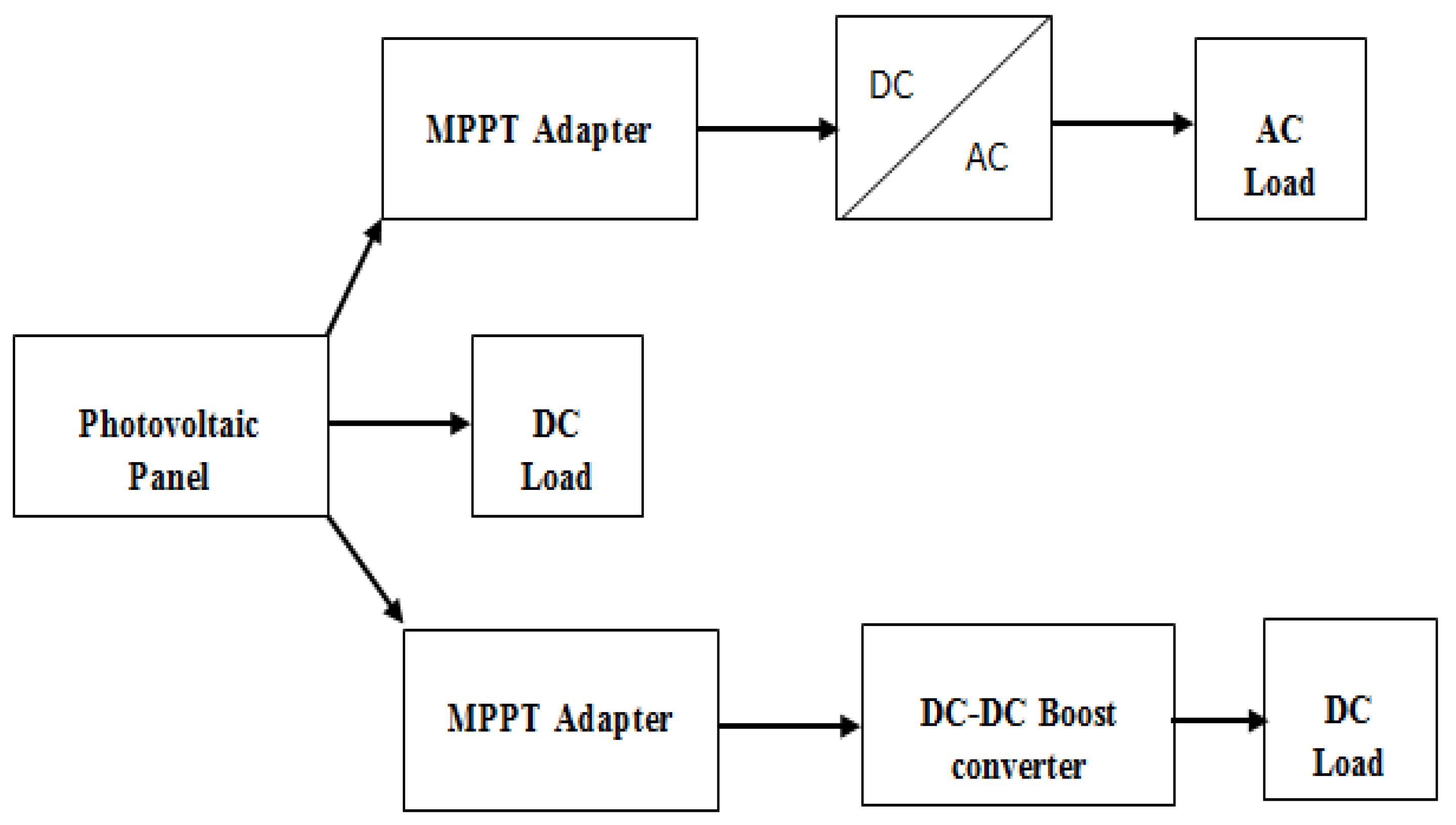
Figure 1 describes stand-alone photovoltaic system types. In most cases, an impedance adaptation must be carried out by inserting an electronic device between the generator and its electrical load which allows the system to be forced to operate at its maximum power. Usually the load is connected to the PV via a DC-DC Boost converter. In addition, DC-DC boost converter is often integrated in both 1ph and 3ph PV inverters for extending their input voltage range ( 150-800 V) for example, therefore, a robust control of this converter must be carried out, and this requires good filtering of the current and voltage signals.
3. Mathematical Model of the PV system
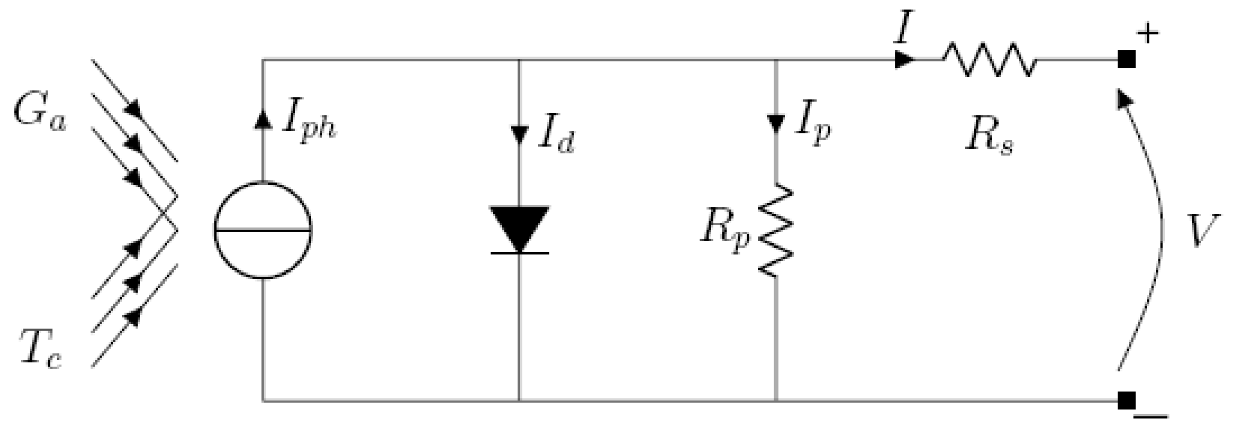
The mathematical model of the photovoltaic panel is obtained using the equivalent circuit of the photovoltaic cell as shows the
Figure 2; A photovoltaic cell is a semiconductor that converts sunlight to electrical power. A cell can be represented by one-diode, two resistance
and
. [
7].
Applying Kirchhoff’s law, The output current can be expressed by:
: is the photocurrent it’s proportional to the solar radiation cell,
is the short-circuit current and its expression is given by:
is the temperature sensitivity, G is the solar irradiance.
The diode current is given by following expression:
Where is the saturation current, q the electron charge ( Coulomb), K is the Boltzman constant (Joule/Kelvin), T temperature cell (Kelvin),
Then, the expression of the total output current can be expressed by:
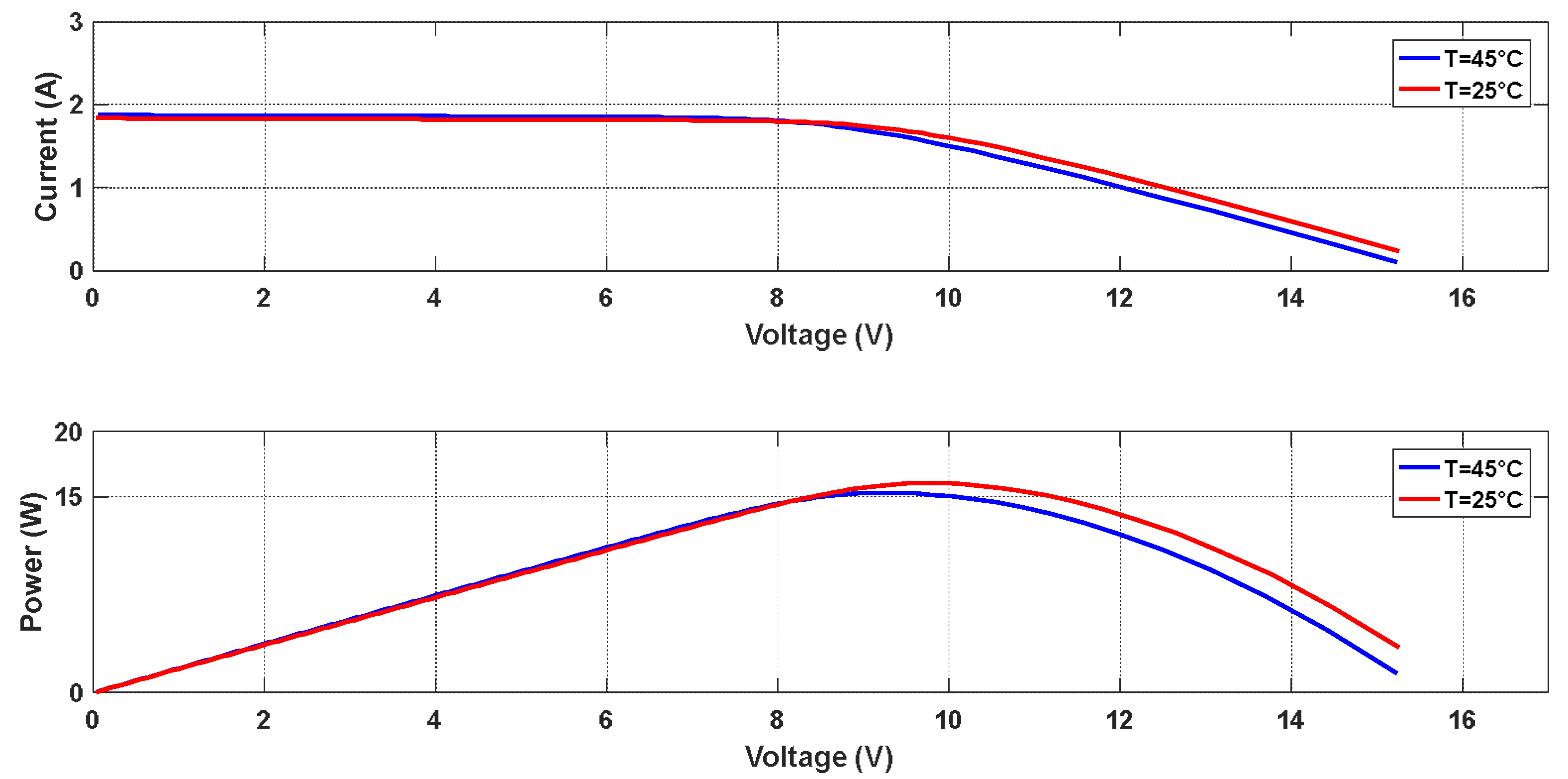
We used Matalab/Simulink software to simulate the photovoltaic panel.
Figure 3 illustrates the current and power curves as a function of voltage
4. DC-DC Boost Converter
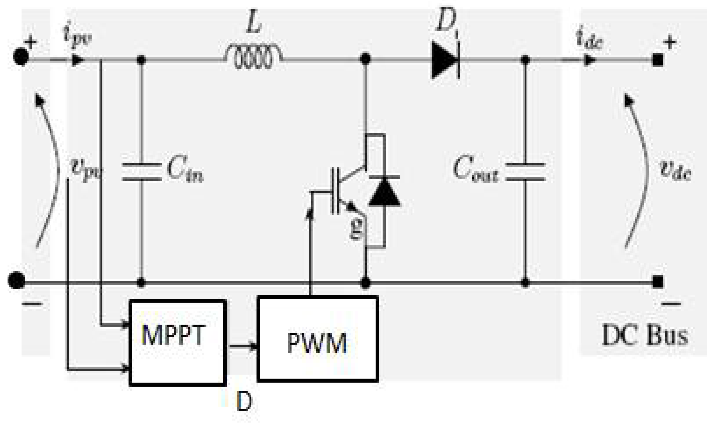
Figure 4 shows the DC_DC boost converter circuit. The converter output voltage is adjusted via the duty cycle of the PWM signal. The Maximum Power Point Tracker (MPPT) adjusts the PV voltage at the maximum power point, for more details see [
8,
9,
10,
11].
The voltage ratio for a boost converter is calculated using the following relationship between the output voltage and the input voltage:
Where: is the total switching period, is the switching off of the IGBT and is the duty cycle.
5. Design of Wavelet Denoiser
The frequency of dynamic signal changes with time, into two ways: slow change and fast change. The slow changing corresponds to the low-frequency part of the signal, representing the main contour of the signal; the fast changing corresponds to the high-frequency part of the signal, In our case, we use the DWT by Mallat algorithm. Which means is if an original signal f(t) is regarded as a discrete approximation
with a resolution of
, it can be decomposed into approximation
with a coarse resolution of
and successive detail approximation
with a high resolution of
such that (
) [
2].
According to the of Mallat algorithm, the rough signal
and detail
at each level can be obtained by
decomposition of the rough signal at the upper level, which is expressed as:
(
) are coefficients of a pair of orthogonals signal filters with different frequency responses, and each wavelet function corresponds to a pair of orthogonal image filters. And each level of rough signal
can be synthesized by the next level of rough signal
and detail
. The composition formula is expressed as:
where h and g are the dual forms of
and
After (
level) decomposition of signal
, a series of wavelet coefficients is obtained expressed by following expression:
After decomposition, the real signal will be concentrated on the large wavelet coefficients. The wavelet coefficients after noise decomposition are generally very small, which is the objective of wavelet transform for noise elimination.
It is assumed that there are m group signals (fX1; 2,/,mg), they are all based on the keyphasor signal, the whole cycle is taken from current sensor and voltage sensor at the output of DC-DC boost convert, so we can design the wavelet transform filter through the following way.
Step 1: normalization of group m signals,
.
Where is the mean value of and is the variance of Step 2: By selecting the same wavelet function and performing discrete wavelet transform on each group of normalized signals, we get m group of wavelet transform coefficients .
Step 3: The wavelet transform filter is given by:
Finally, to realize the wavelet Denoiser, the original signal
(current
or voltage
) is first transformed into discrete wavelet, and then the resulting wavelet coefficient C(t) is multiplied by the wavelet transform filter H, which can be expressed as:
The filtered signal can be obtained by inverse wavelet transform of
[
2].
6. Experimental Results
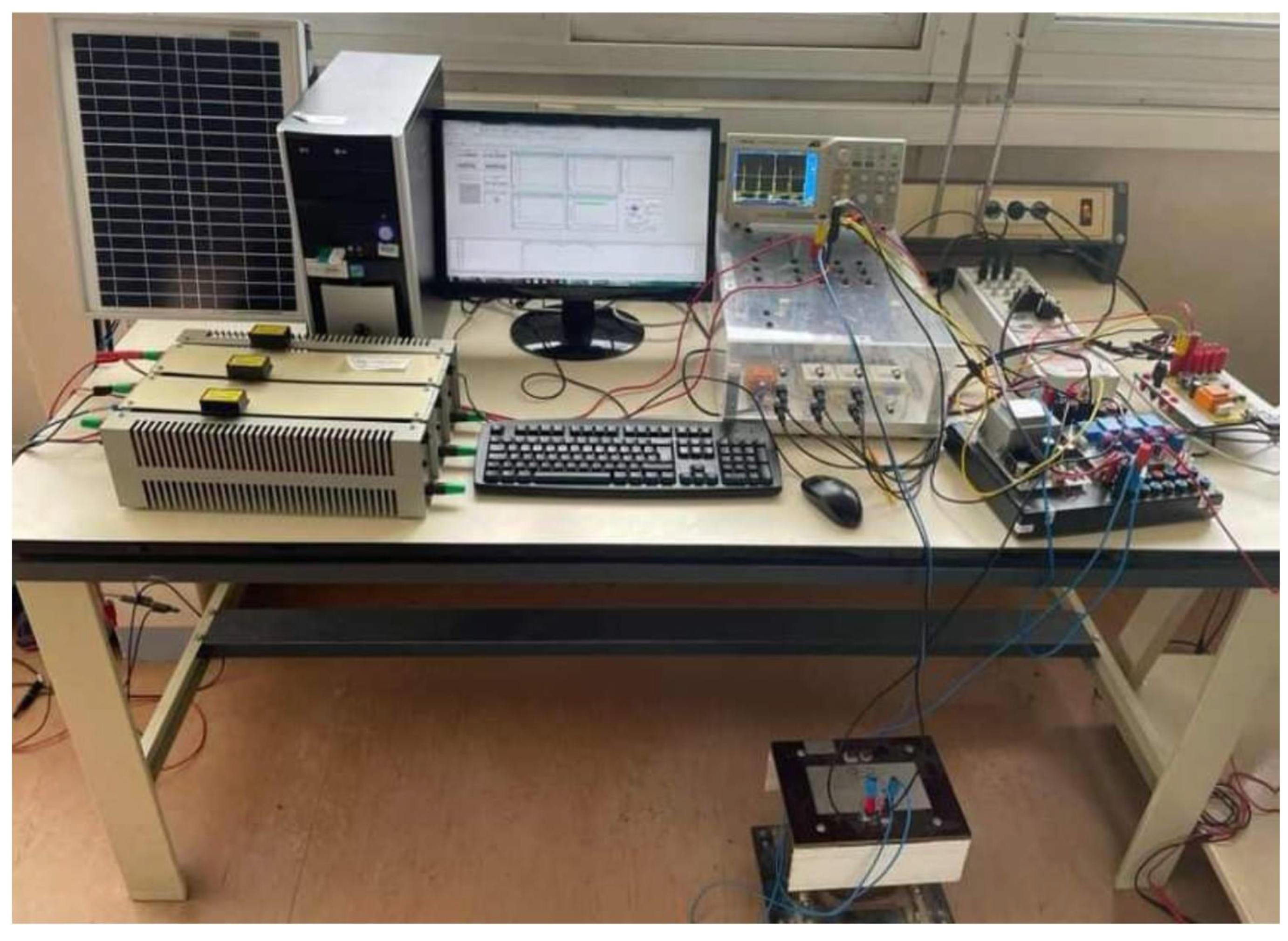
Figure 5 shows the experimental test bed at Jules Verne Picardie University. It contains a DSP-RTI 1104, a DC-DC boost converter, a PV panel, a current sensor, a voltage sensor, and a load.
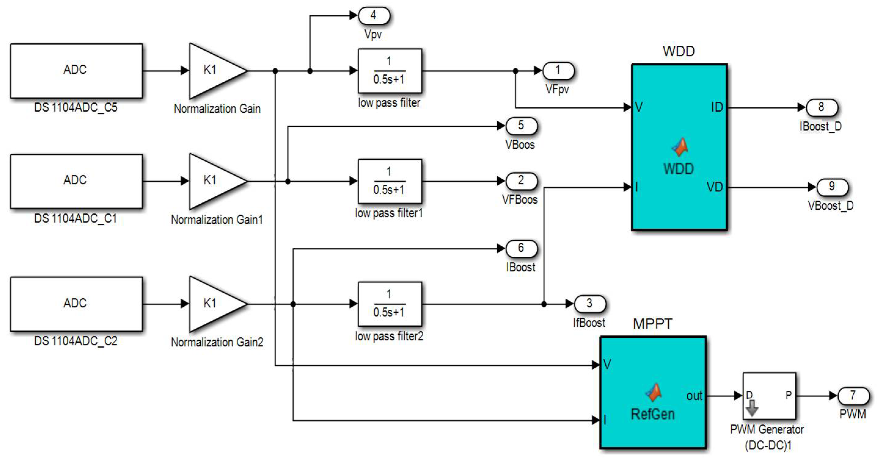
Figure 6 represents the signal acquisition diagram in Matlab / Simulink.
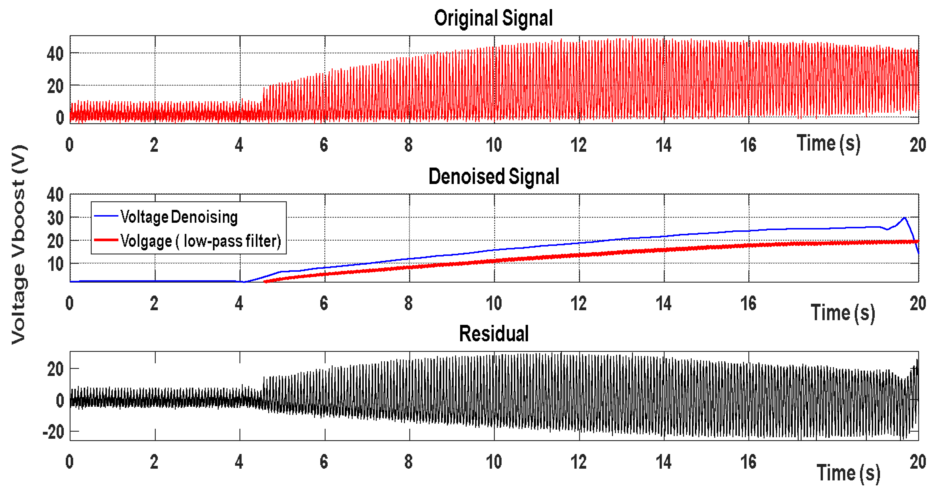
Figure 7 shows the voltage signal with noise.
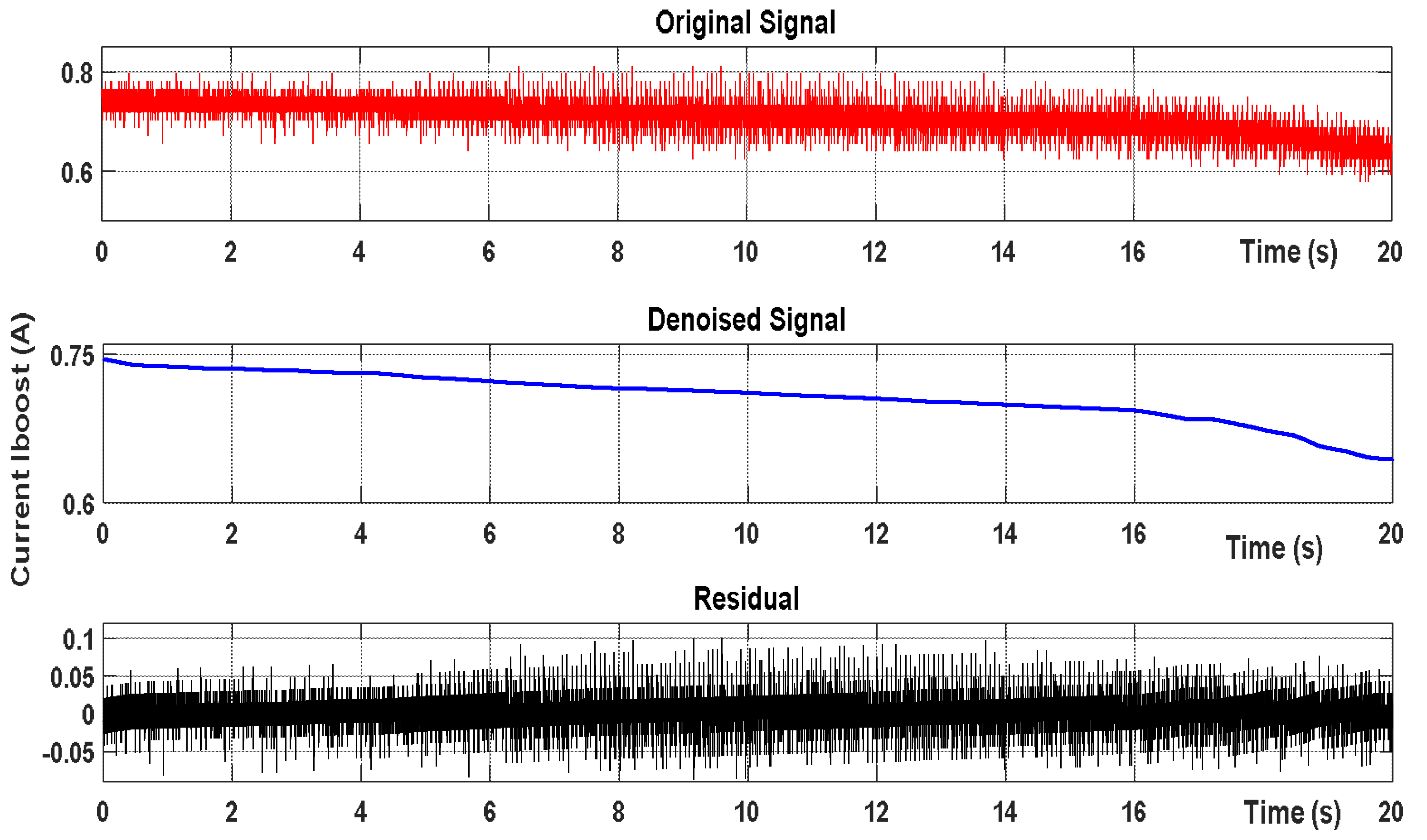
Figure 8 shows the current signal with noise. Figure 9 shows the waveform processed by the proposed discrete wavelet denoising algorithm (WDD). It can be seen that the denoising method can eliminate the noise in the noise impact signal due to sensors. In order to validate the denoising by our method, we compare the characteristics with those obtained by a classical low-pass filter, as shown in figures 7 and figure 8.
The characteristics obtained by denoising signals seem to be really better than those obtained by classic filtering, this clearly shows the superiority of our proposed WDD system. We can clearly see in
Figure 7 that the current shape seems to be perfect.
Figure 8 illustrates the voltage-shaped e signal before and after filtering by the two methods. The obtained signal by our proposed method appears better than that obtained by the low-pass filter, both in terms view point amplitude and shape. And thus we can say filtering by denoising does not lose either the signal nature or power, which represents our objective.
6. Conclusion
In this work, we present the simple structure of a photovoltaic system. We gave an overview of the Mallat algorithm on which our WDD Denoiser is based. The results obtained are very satisfactory, which encourages us to apply this famous Denoiser to other delicate control systems. Finally, we suggest introducing artificial intelligence ( fuzzy logic, genetic algorithm, neural network……..) for the control of systems more delicate than this.
References
- Graps, “An introduction to wavelets”, IEEE Computational Science and Engineering ( Volume: 2, Issue: 2, Summer 1995).
- Feng Miao, Rongzhen Zhao,” A new method of vibration signal denoising based on improved wavelet”, Journal of Low Frequency Noise, Vibration and Active Control 2022, Vol. 41(2) 637–645.
- Selesnick IW, ” Wavelet transform with tunable Q-factor”, IEEE Trans Signal Proc 2011; 59(8): 3560–3575.
- Hao Xie, Xi Tian, Kejou Zhang, ” Noise Reduction Method Based on the Wavelet Analysis for RF side-channel Signals” , 2022 Global Conference on Robotics, Artificial Intelligence and Information Technology (GCRAIT).
- Ajith Ashok, Gayathri K S, Aneela Babburi, Indu R J, Ardra T, Gayathri Narayanan, “ Performance comparison of matched filter, wavelet denoising and wiener filter technique in communication receivers”, 2018 3rd IEEE International Conference on Recent Trends in Electronics, Information & Communication Technology (RTEICT-2018), MAY 18th & 19th 2018.
- Sylvain Sardy, Paul Tseng, and Andrew Bruce,” Robust Wavelet Denoising”, IEEE TRANSACTIONS ON SIGNAL PROCESSING, VOL. 49, NO. 6, JUNE 2001.
- AngalaesWari.S, Jamuna.K,Sanjeevikumar Padmanaban, Baseem Khan, “Design and implementation of a robust of iterative learning controller for voltage and frequency stabilization of hybrid microgrids “, Computer & Electrical Engineering, 84(2);106631. [CrossRef]
- D. E. Zabia, H. AfghoulO. Kraa, “Maximum Power Point Tracking of a Photovoltaic System Under Partial Shading Condition Using Whale Optimization Algorithm”, International Conference on Artificial Intelligence in Renewable Energetic Systems, IC-AIRES 2021.
- 9. Yakhlef Riheb; Bchir Riadh; Khoja Intissar; Taoufik Ladhari,” MPPT Control Of Photovoltaic Panel Based On Artificial Neural Network 2023 IEEE International Conference on Artificial Intelligence & Green Energy (ICAIGE). [CrossRef]
- M. Kamran, M. Mudassar, M. Rayyan Fazal, M. Asghar, M. Bilal, R. Asghar, “Implementation of improved Perturb & Observe MPPT technique with confined search space for standalone photovoltaic system”, Journal of King Saud University – Engineering Sciences, 2018.
- AngalaesWari.S, Jamuna.K,Sanjeevikumar Padmanaban, Baseem Khan, “Design and implementation of a robust of iterative learning controller for voltage and frequency stabilization of hybrid microgrids “, Computer & Electrical Engineering, 84(2);106631. [CrossRef]
|
Disclaimer/Publisher’s Note: The statements, opinions and data contained in all publications are solely those of the individual author(s) and contributor(s) and not of MDPI and/or the editor(s). MDPI and/or the editor(s) disclaim responsibility for any injury to people or property resulting from any ideas, methods, instructions or products referred to in the content. |
© 2024 by the authors. Licensee MDPI, Basel, Switzerland. This article is an open access article distributed under the terms and conditions of the Creative Commons Attribution (CC BY) license (http://creativecommons.org/licenses/by/4.0/).
