Preprint
Article

Long Electrical Stability on Dual Acceptor P-Type ZnO:Ag,N Thin Films

Altmetrics

Downloads

99

Views

42

Comments

0

A peer-reviewed article of this preprint also exists.

Submitted:

09 May 2024

Posted:

09 May 2024

You are already at the latest version

Alerts
Abstract
p-type Ag-N dual acceptor doped ZnO thin films with long electrical stability were deposited by DC magnetron reactive co-sputtering technique. After deposition, the films were annealed at 400 °C for one hour in a nitrogen-controlled atmosphere. The deposited films were amorphous. However, after annealing they crystallize in the typical hexagonal wurtzite structure of ZnO. The Ag-N dual acceptors were incorporated substitutionally in the structure of zinc oxide and achieving that the three samples presented the p-type conductivity in the ZnO. Initial electrical properties showed a low resistivity of from 1 to10^{−3} Ω.cm, Hall mobility of tens cm2/V.s and a hole concentration from 10^{17} to 10^{19} cm^{−3}. The electrical stability analysis reveals that the p-type conductivity of the ZnO:Ag,N films is very stable and does not revert to n-type, even after 36 months of aging. These results reveal the feasibility of using these films for applications in short-wavelength or transparent optoelectronic devices.
Keywords: 
Subject: Chemistry and Materials Science  -   Electronic, Optical and Magnetic Materials

1. Introduction

The increasing interest that has emerged in the development of short-wavelength optoelectronic devices, based on transparent semiconductors, has generated the demand for the use of group II-VI semiconductors. In recent years, ZnO has been considered as a promising semiconductor for the development of transparent conductive materials since it has a direct bandgap of 3.3 eV, and low threshold voltage devices. Moreover, it is well known that ZnO has a large number of advantages over AlN and GaN, two commonly used semiconductors in the short-wavelength optoelectronics industry [1,2,3]. Some of these advantages include a large exciton energy (60 MeV), which can lead to violet and UV sources with high brightness and lower power thresholds at room temperature. The ZnO has greater resistance to radiation than the Si, GaAs, CdS, and GaN, therefore, it enhances its use for space applications.
Well knows that undoped ZnO shows n-type conductivity. Some studies suggested that this conductivity is due to the presence of hydrogen in the structure, which works as a donor with a very low ionization energy (30 meV) [4,5]. This behavior due to hydrogen tends to diffuse very easily in large quantities into the structure of ZnO, and in turn, it is present in all the techniques used for the deposition of ZnO thin films. Despite the extensive amount of work reported on p-type thin films deposited by different techniques and with different doping elements, which may enter in substitution of oxygen or zinc, a reliable electrical conductivity for p-type ZnO has not yet been achieved [6,7,8,9,10].
Therefore, this subject is of great interest to the scientific community of materials science since for developing ZnO based optoelectronic devices the principal difficulty lies and has been the manufacture of p-type thin films with good crystalline quality and acceptable electrical stability. The lack of stability is mainly due to the low solubility of the acceptor dopants, the depth of the acceptor level, and the compensation effect between the acceptor and native ZnO donor dopants [1,5,11,12]. Within all the experimental methodologies addressed for the manufacture of p-type ZnO, the double doping method, in which the dopant can be either a double acceptor (acceptor-acceptor) or acceptor-donor, has proved to be the best channel to overcome these difficulties. The double-doping method using two acceptor agents to prepare p-type ZnO, Li-N [13,14], Ag-Li [15] or Cu-N [16] dopants have been recently investigated. Additionally, experimental publications have been reported on the manufacture of p-type ZnO:Ag,N thin films with good electrical properties obtained by the ultrasonic pyrolytic spray technique [17,18,19,20]. Similarly, there are new reports using the technique of deposition by assisted ion implantation [21], the sol-gel and spin coating methods [22,23] and sputtering method [24]. At the same time, theoretical investigations suggest that Ag and N are the two best candidates for the production of p-type ZnO, taking into account the effects of deformation and substitution energy levels of Ag-Zn and N-O [25,26,27].
In this paper, there is presented a study of the electrical stability of p-type ZnO:Ag,N thin films deposited by DC reactive magnetron co-sputtering method. After 36 months of aging, the electrical stability analysis reveals that the p-type conductivity of the ZnO:Ag,N films is very stable and does not revert to n-type.

2. Materials and Methods

Ag and N double acceptor doped ZnO thin films were deposited on GaAs (100) substrates by DC magnetron co-sputtering reactive method, using metallic targets of zinc and silver as precursors, both of two inches in diameter and a purity 99.99 %. Previously to the deposit process, the growth chamber was evacuated until reaching a base pressure of 8.7x10⁻⁷ Torr. The deposits were made at a working pressure of 6x10⁻³ Torr, and the sputtering reactive atmosphere was composed by 5 sccm of argon (99.995%), 15 sccm of nitrogen (99.999 %) and three different oxygen (99.999 %) flows of 2 sccm, 2.5 sccm, and 3 sccm, respectively. All films were deposited at room temperature (approx. 25 °C) with a power density of 4 W/cm2 and 1.5 W/cm2 in zinc and silver targets, respectively. The target-substrate distance was 10 cm and 15 cm for Zn and Ag, respectively. In order to control the percentage of silver incorporated in the film during the growth process, the shutter for the silver target was opened intermittently, with a period of only one second open for every 20 seconds of deposit. After growth, the samples were thermally treated at 400 °C for 1 hour in a nitrogen atmosphere. To determine the elemental composition of the samples, the films were characterized in a Jeol Scanning Electron Microscope, model JSM-6390LV, which is equipped with an Energy Dispersion Spectrometer (INCA X-sight Oxford Inst. Model 7558). The crystalline structure of thin films ZnO unpurified with Ag and N was studied in a D-5000 Diffractometer from Siemens using the Cu K alpha radiation line with a wavelength (0.1541 nm). The concentration of charge carriers were determined by Hall Effect in an Ecopia HMS-3000 measurement system, using the Van der Pauw method.

3. Results

3.1. Elemental Composition
Through the results of X-ray Dispersed Energy Spectroscopy, the presence of zinc, oxygen, nitrogen, and silver was measured in all films deposited and thermally treated. The atomic concentrations obtained for each film are shown in Table I. According to these values, all the samples present a slightly higher concentration of oxygen, in which a maximum value of 58.30 % is observed for the films with a gas flow ratio of 5/2.5/15. On the other hand, the atomic concentration of Zn was less than 40 %, with a minimum value of 36.28 % for the film deposited with an oxygen flow of 3.0 sccm. The atomic percentage of nitrogen incorporated in the samples varies from 3.78 to 4.65 at. % as the flow of oxygen present in the reactive atmosphere decreases. Additionally, as the percentage of nitrogen in the sample increases, so does the percentage of silver incorporated in the different films, as can be seen in Table 1.
Figure 1 shows the X-ray diffraction patterns of ZnO:Ag,N films. In all diffractograms, seven characteristic peaks of the ZnO wurtzite hexagonal structure are observed; these peaks are centered at 31.78, 34.48, 36.38, 47.59, 56.46, 62.64, and 67.72 2θ degrees, which correspond to the diffraction planes (100), (002), (101), (102), (110), (103) and (200) respectively. High intensity is observed for the (002) diffraction peak for the film deposited under a reactive atmosphere with 2.0 sccm of oxygen, indicating that the films have a preferential crystalline orientation along the c-axis perpendicular to the surface of the substrate. However, this condition is lost for the rest of the samples, which showed similar intensities for the peaks centered at 34 and 36 degrees and associated to (002) and (101) planes, respectively. As are showed in the diffractograms, in the case of the samples deposited at a higher concentration of oxygen the intensity of the (002) peak is gradually decreased, while the peak associated with the plane (101) increases. The leftover peaks presented in the diffraction patterns remain virtually unchanged.
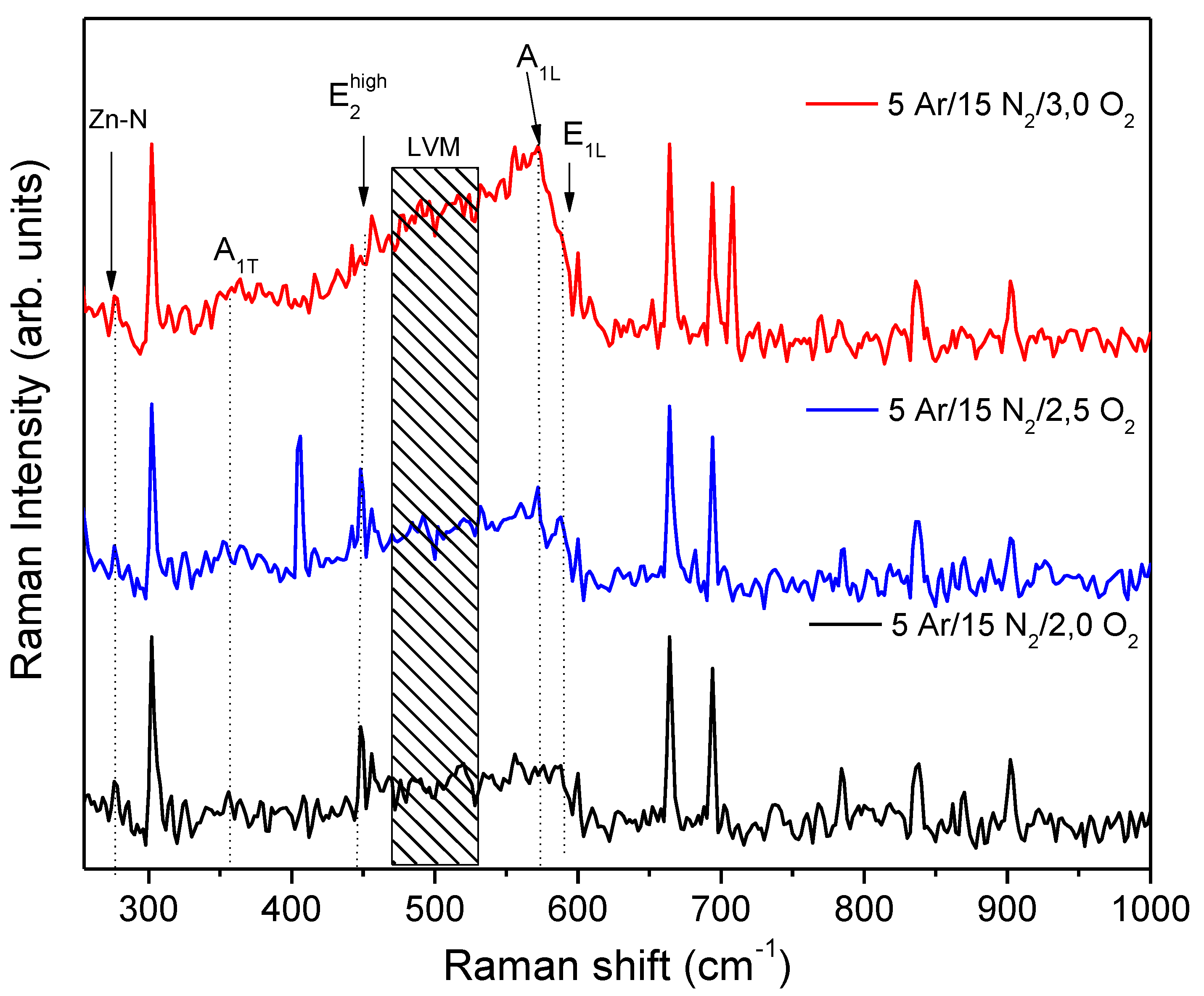
In Figure 2 the vibrational properties of the p-type ZnO:Ag,N thin films are presented. According to group theory, for the perfectly crystalline ZnO (wurtzite hexagonal structure belongs to the P63mc space group), the optical modes that should exist in the ZnO with wurtzite structure are given by the equation:
Γ o p t = A 1 + E 1 + 2 E 2 + 2 B 1
where modes A1 and E1 are polar modes, with optical transverse splitting (A1T and E1T) and longitudinal optical splitting (A1L and E1L), while modes E2 are non-polar modes and consists of two modes with low and high frequency denoted as E2low and E2high, respectively. The former modes are known as active modes. Finally two modes B1 are presented which are silent. Modes E2low, E2high, A1T, A1L, E1T, and E1L are located at 101, 447, 381, 574, 407, and 583 cm-1, respectively. Now, analyzing the obtained Raman spectra, the dominant peak indicated in the Raman spectra as E2high is observed at 447 cm-1. This signal corresponds to the more characteristic phonon of the Wurtzite hexagonal structure of the ZnO. The peak positioned at 573 cm-1 is associated with the A1L mode and finally, the peak positioned at 589 cm-1 could be associated with the E1L optical mode and it is attributed to the formation of defects such as the absence of oxygen and zinc interstitial [28,29]. The additional peak observed at 274 cm−1, in the Raman spectrum, can be attributed to the vibration of Zn atoms, where some of its first nearest neighbor oxygen atoms are replaced by nitrogen atoms in the hexagonal structure [30]. Additional local vibrational modes (LVM) in the range from 460 to 520 cm−1 can be observed in the Raman patterns of ZnO:Ag,N films. These LVM are explained due to the defects induced by impurities break the translational symmetry of the crystal [31]. A particular mode centered at 493 cm−1 has been reported to be related to the Ag atoms when they replaced the Zn atoms in the ZnO structure [32]. Then, after analyzing the Raman patterns for the ZnO:Ag,N thin films, the presence bands located at 274 and 493 cm-1 confirms that the impurities have been incorporated substitutionally into the ZnO wurtzite hexagonal structure.
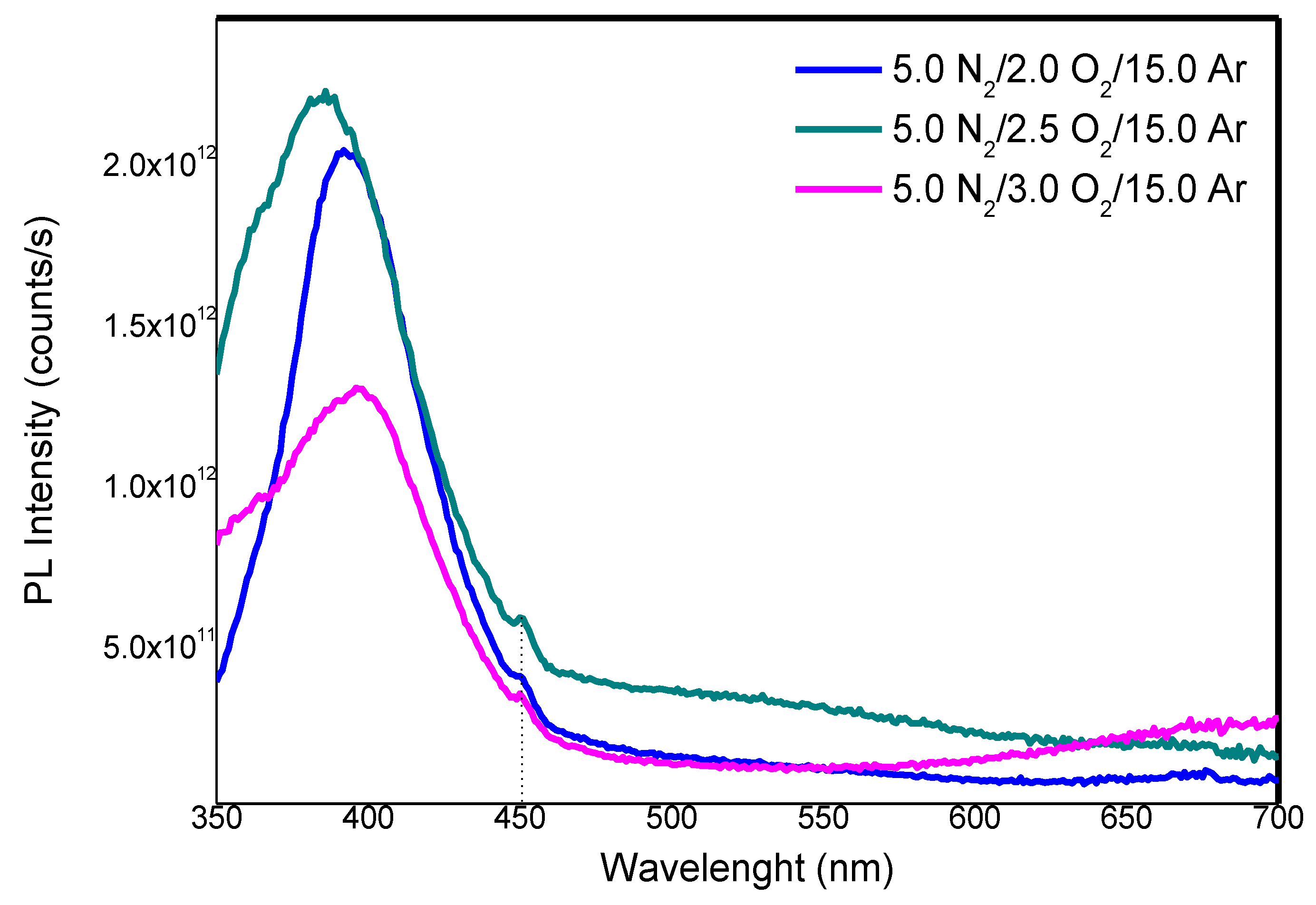
Figure 3 shows the photoluminescence (PL) spectra, measured at room temperature, of the ZnO: Ag, N films. In all three PL spectra a very strong ultraviolet emission is observed near the edge of the band (NBE) and is related to free exciton recombination. This peak of ultraviolet emission shows a direct dependence as a function of the total concentration of dopants. For the film with a lower dopant concentration, the peak is centered at 383 nm (3.23 eV), however, the edge of this emission band shifts towards higher wavelengths (lower energies) as the dopants atomic percentage increases. For the other two samples, the UV emission peaks are centered at 393 nm (3.15 eV) and 397 nm (3.12 eV), respectively. Generally, ZnO has an emission band in the green region related to deep-level emission. This emission is linked to the formation of intrinsic defects such as interstitial zincs and oxygen vacancies, which act as donor defects. In the three samples studied, it can be observed that this emission is very weak compared to the emission in the ultraviolet, that is, there is a low density of native defects, which is in good agreement with the results of XRD and Raman results.
The characterization of the ZnO:Ag,N thin films by Hall Effect in Van Der Pawn configuration, indicates that all the studied samples exhibit a p-type conductivity, with relatively high densities of charge carriers as showed in Table 2. According to the values obtained, it can be seen that the film deposited at a lower concentration of oxygen presents a lower carrier density. Moreover, the concentration of charge carriers increases as the oxygen ratio in the sputtering atmosphere increases. This behavior can be explained if there is considered that in O-poor the incorporation of nitrogen and silver is favored, and with this the acceptor levels generated with the substitution of zinc and oxygen by silver and nitrogen respectively.
In order to verify the stability in time of the p-type conductivity of the ZnO: Ag, N thin films the electrical measurements were carried out once the samples were deposited and after 12 and 36 months of aging. During this time, the samples were stored at atmospheric pressure in ordinary individual plastic containers.
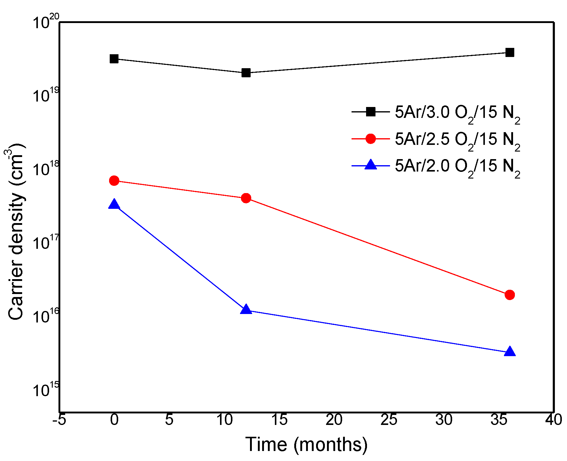
As seen in Figure 4, after 36 months all samples still sustain p-type conductivity. For the film deposited at a higher oxygen concentration, a slight decay of almost an order of magnitude in the free carrier density is observed. On the other hand, for the other two studied samples, practically the same values for the hole concentration ​​were obtained after that the 36 months have elapsed. This result shows that ZnO:Ag,N films had a minimal deterioration in their electrical properties, that is to say, that the free carrier density is practically constant, in particular for films deposited at a flow of 5 sccm of Ar, 3 sccm of O2 and 15 sccm of N2. Finally, the results ensure that the p-type conductivity of ZnO:Ag,N films is very stable and does not revert to type n, even after 36 months, as is usually the case with simple doped ZnO:Ag or ZnO:N. According to these results, we can thus affirm that the deposited films maintain the electrical properties almost without evident degradation, which reveals that the self-compensation introduced by intrinsic defects in the films is suppressed due to the double acceptor doping.
Figure 4. Carrier concentration of the p-type ZnO:Ag,N thin films as a function of aging time, measurements were made when it was deposited (0 months), at twelve months and after 36 months elapsed.
Preprints 106043 g004
Using the wurtzite ZnO unit cell as the elemental basis, the unit cell (4 atoms) and 5 supercells (with 32 atoms each) were used ZnO pure and doped. This method is implemented and fully integrated in the QUANTUM ESPRESSO suite of codes [33,34] (www.quantum-espresso.org) for plane wave and norm-conserving pseudopotentials [35,36]. The exchange-correlation potential was determined using the generalized gradient approximation considering the Perdew-Burke-Ernzerhof scheme (GGA-PBE). The electron wave function was expanded in plane waves with a cut off Energy of 80 Ry (1088.5 eV), and 560 Ry (4353.8 eV) for the charge. The used Monkhorst-Pack grid was 6 X 6 X 4 for the irreducible Brillouin zone sampling. Self-consistency in total energy was achieved with a tolerance of less than 10-6 Ry (1.36 x 10⁻⁵ eV).
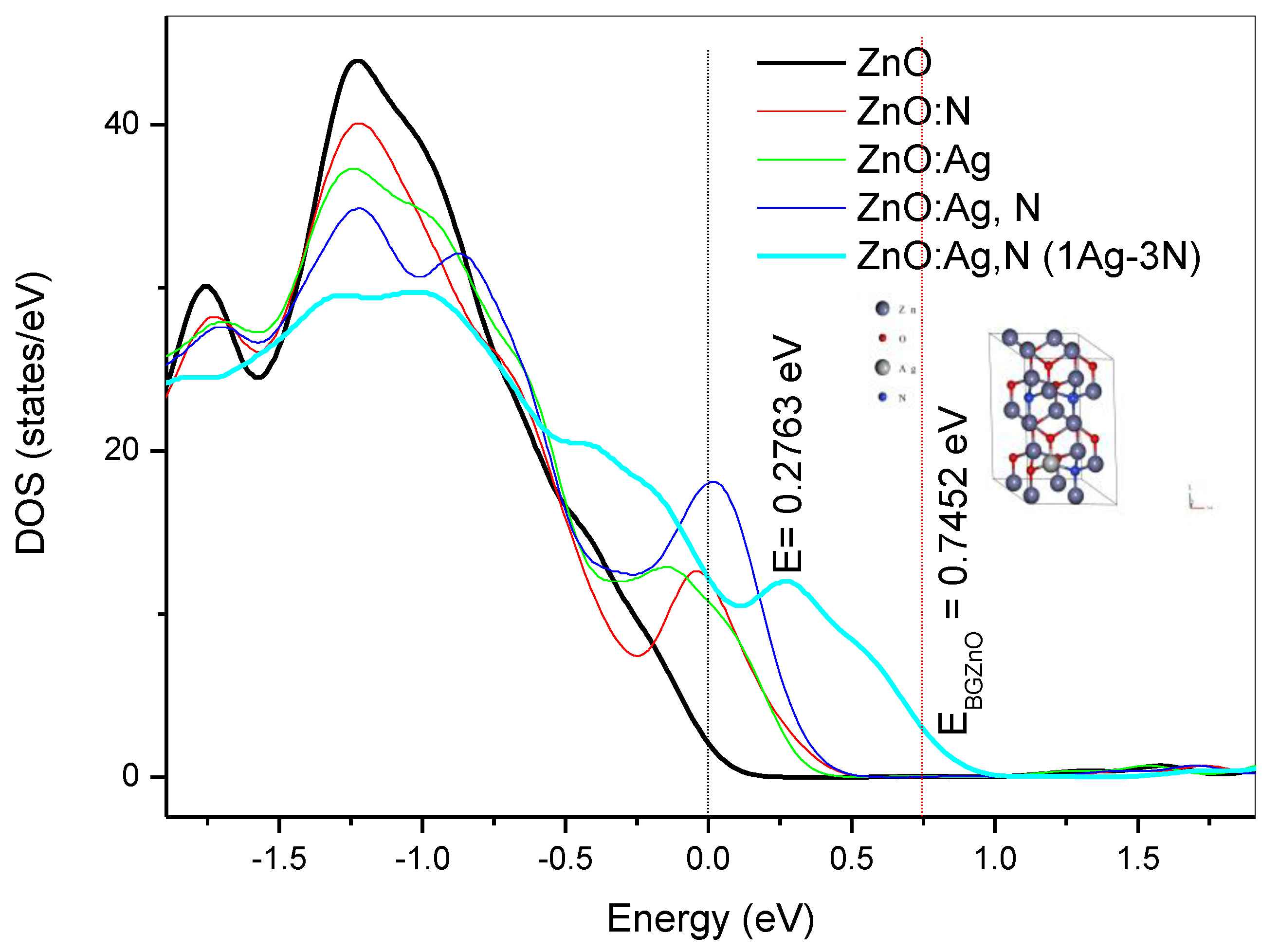
For the analysis, firstly, it can be shown how the density of states is affected by the presence of the impurities, Figure 4. As the impurities are integrated, neat to the top of the valence band, in the band gap, there are states associated to nitrogen, silver and the hybridization of both (N and Ag) with the Zinc and the oxygen. The major effect is when both impurities are integrated to the structure. It can be shown than the principal value (maximum) is located below the mid-half of the band gap, it means, they are shallow type p-doping impurities, as it was been reported before. This is evidence of why the structure has enough p-type carriers to remain stable and not reverse as has been reported in other cases.
Figure 4. Effect of the impurities on the Density of states for the different single and dual doped p-type zinc oxides compounds.
Preprints 106043 g005
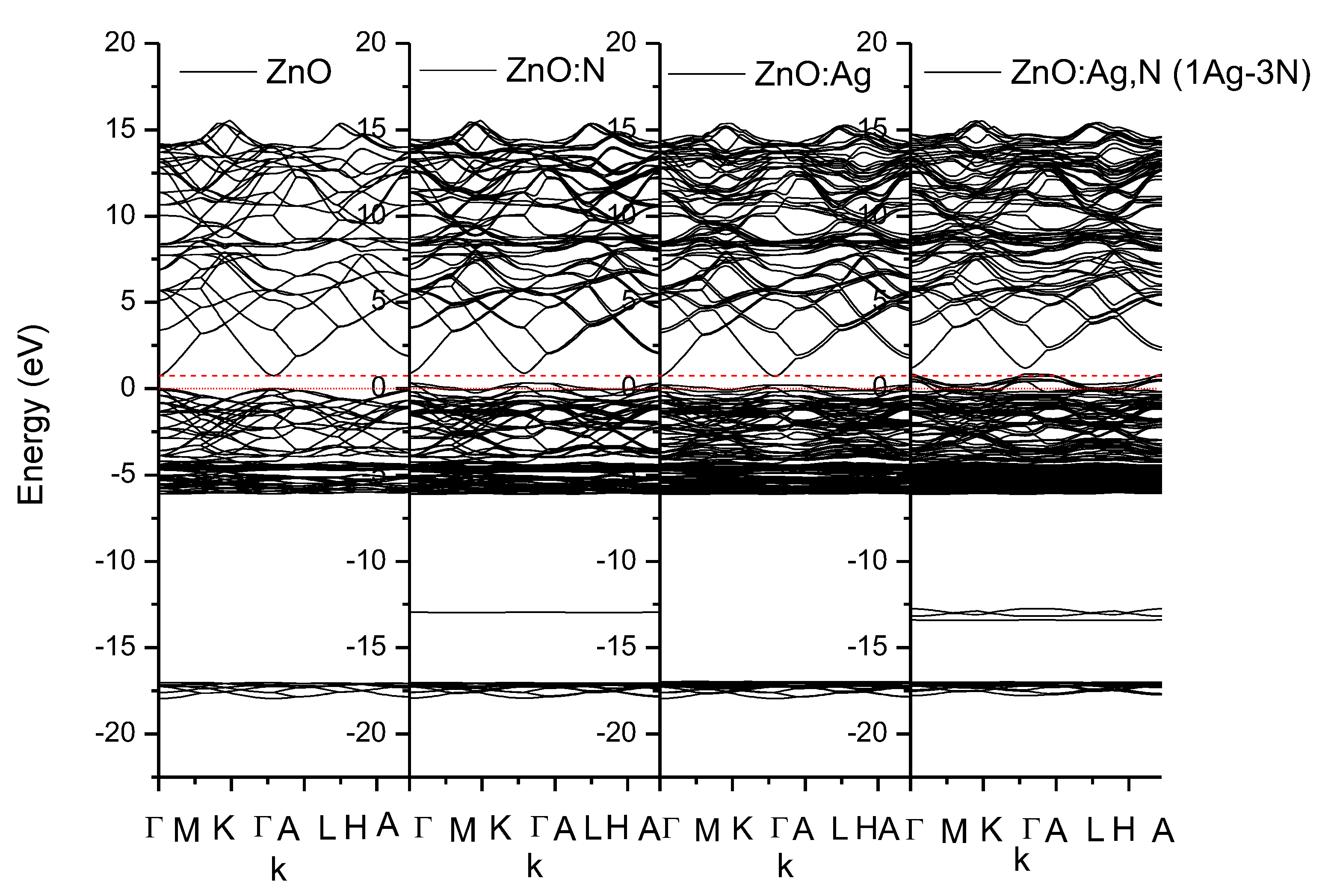
The effect of the impurities in the band structure is evident in Figure 5, where there are 4 zone bands: the first is associated to the O2s, around the -17 to the -15 eV. The second, very subtle, due to the N2s contributions, around the -13 to the -12 eV, the principal associated to the Zn3d, O2p and Ag 4d, ending in the 0eV for ZnO, and the effects due to hybvridizations among Zn, O, N and Ag with their hybridizations. The conductance is the upper band, and it is due principally to Ag 5d, Zn 4d, N 2p and O 2p. The bands are forced, as impurities are integrated, to have higher energy values. It can be shown in Figure 5.

4. Conclusions

ZnO:Ag,N films annealed at 400 °C are crystalline with a wurtzite hexagonal structure typical for ZnO. As a result of the incorporation of the double acceptor agent, the films have p-type conductivity. Silver and nitrogen enter the structure as substitutes for zinc and oxygen respectively forming Ag-Zn and N-O acceptor sites, whereby a double contribution is generated for the creation of holes, thereby achieving a high density of holes. The electrical stability analysis reveals that the p-type conductivity of ZnO:Ag,N thin films is very stable and it do not revert to n-type, even after 36 months, as is usual in the case with simple doped ZnO:Ag or ZnO:N. According to these results it is possible to affirm that ZnO:Ag,N films, deposited and annealed at 400 °C, maintain the electrical properties almost without evident degradation, which reveals that the self-compensation introduced by intrinsic defects in the films is suppressed due to double acceptor doping.

Declaration of interest statement

As authors of the present manuscript, we declare that: We have not affiliations with or involvement in any organization or entity with any financial interest or non-financial interest in the subject matter or material discussed in this manuscript, which may constitute a conflict of interest, whether real, potential or apparent.

Author Contributions

Conceptualization, J.J.O.S. and J.J.A.; methodology, J.J.O.S. and F.A.M.; software, J.J.A. and J.A.V.T; validation, A.A.O.H., J.A.B.T and H.A.D.M.; formal analysis, J.J.O.S. , F.A.M., R.G.R, and J.J.A.; investigation, F.A.M., R.G.R, and J.A.B.T; resources, J.J.O.S. and V.H.M.G.; data curation, J.A.V.T. and H.T.H.; writing—original draft preparation, J.J.O.S., R.G.R. and F.A.M.; writing—review and editing, J.J.O.S., A.A.O.H., and H.A.D.M.; visualization, V.H.M.G. and H.T.H.; project administration, J.J.O.S.; funding acquisition, V.H.M.G., J.J.O.S. and J.J.A.

Funding

This work was partially supported by Projects UAZ-PTC-205 and PFCE-UAZ-2018-2019.

Acknowledgments

The authors are grateful to Marcela Guerrero and Angel Guillen from the Department of Physics of the CINVESTAV for the characterization of the samples and their technical assistance.

References

  1. Ozgur, U.; Ya. I; Alivov, C; et al.; A comprehensive review of ZnO materials and devices. J. Appl. Phys, 2005, 98, 041301. [CrossRef]
  2. Hwang, D.K; Oh, M. S; Lim, J. H; and Park, S. J; ZnO thin films and light-emitting diodes, J. Phys. D: Appl. Phys, 2007, 40, R387–R412. [CrossRef]
  3. Rekha, S. M; Neelamana, H. V; and Bhat, S. Recent Advances in Solution-Processed Zinc Oxide Thin Films for Ultraviolet Photodetectors, ACS Applied Electronic Materials. 2023; 5, 4051–4066. [Google Scholar] [CrossRef]
  4. Ip, K; Overberg, M.E; Heo, Y. W; et al.; Hydrogen incorporation, diffusivity and evolution in bulk ZnO, Solid-State Electron. 2003, 47, 2255–2259. [CrossRef]
  5. Janotti A; de Walle, C.G.V; Fundamentals of zinc oxide as a semiconductor. Rep. Prog. Phys. 2009, 72, 126501. [CrossRef]
  6. Yang, R; Wang, F; Lu, J; et al. ; ZnO with p-Type Doping: Recent Approaches and Applications ACS Applied Electronic Materials, 2023, 5, 4014–4034. [CrossRef]
  7. Brauer, G; Kuriplach, J; Ling C.C; Djurisic, A. B; Activities towards p-type doping of ZnO, J. Phys.: Conf. Ser, 2011, 265, 012002. [CrossRef]
  8. Regalado-Contreras, A.; Farías, M.H.; De La Cruz, W. Room temperature deposition of stable p-type ZnO:N thin films through chemical species modulation using reactive pulsed laser deposition. Applied Surface Science, 2023; 640, 158393. [Google Scholar] [CrossRef]
  9. Silva, ALC; Vargas, LMB; Peres, ML; et al. ; Exploring Na Doping in ZnO Thin Films: Electrical and Optical Insights. Coatings. 2024, 14, 510. [CrossRef]
  10. Çavdar, Ş; Şahin, V; Turan; N; et al; Structural and electrical characterization of Cd-doped ZnO thin films produced on p-type Si substrate by SILAR technique. J Mater Sci: Mater Electron 2023, 34, 1787.
  11. Ellmer and Bikowski, A. ; Intrinsic and extrinsic doping of ZnO and ZnO alloys, J. Phys. D: Appl. Phys, 2016, 49, 413002. [Google Scholar] [CrossRef]
  12. Jessadaluk, S.; Khemasiri, N.; Kayunkid, N.; et al. ; Influence of Antimony Species on Electrical Properties of Sb-Doped Zinc Oxide Thin Films Prepared by Pulsed Laser Deposition. Nanomaterials, 2023, 13, 1799. [Google Scholar] [CrossRef]
  13. Lu, J. G.; Zhang, Y. Z.; Ye, Z. Z.; et al. ; Low resistivity, stable p-type ZnO thin films realized using a Li and N dual acceptor doping method, Appl. Phys. Lett, 2006, 88, 222114. [Google Scholar] [CrossRef]
  14. Duan, X.Y.; Yao, R. H. ; and Zhao; Y. J., The mechanism of Li,N dual-acceptor co-doped p-type ZnO, Appl. Phys. A, 2008, 91, 467–472. [Google Scholar] [CrossRef]
  15. Das, A; Basak, D (Ed.) Mechanism of converting n-type to p-type conductivity in ZnO nanorods array films co-implanted with nitrogen and lithium ions, Materials Science and Engineering: B, 2023, 298, 116860. [Google Scholar] [CrossRef]
  16. Rahman, M.; Kamruzzaman, M.; Zapien, J.A. ; et. al.; Conversion of n-type to p-type conductivity in ZnO by incorporation of Ag and Ag-Li, Materials Today Communications, 2022, 33, 104278. [Google Scholar] [CrossRef]
  17. Md Nurul, H.L.; Abu Kalam, M. F. ; Md Kamruzzaman; et.al.;Dual acceptor (N, Cu) doping effects on the electronic and optical properties of ZnO. Materials Chemistry and Physics, 2020, 242, 122463. [Google Scholar] [CrossRef]
  18. Bin, W; Yue, Z; Jiahua, M; et al. ; Ag N dual accept doping for the fabrication of p-type ZnO. Appl. Phys. A, 2009, 94, 715–718. [CrossRef]
  19. Swapna, R; Santhosh-Kumar, MC; Deposition of the low resistive Ag N dual acceptor doped p-type ZnO thin films, Ceram. Int. 2013, 39, 1799–1806. [CrossRef]
  20. Swapna, R; Amiruddin, R; Santhosh-Kumar, MC; Aging and annealing effects on properties of Ag-N dual acceptor doped ZnO thin films. AIP Conf. Proc. 2013, 15, 682. [CrossRef]
  21. Jing-Wei, W; Ji-Ming, B; Hong-Wei, L; et al. ; Enhanced p-Type ZnO Films through Nitrogen and Argentum Codoping Grown by Ultrasonic Spray Pyrolysis. Chin. Phys. Lett. 2008, 25, 3400. [CrossRef]
  22. Yan, Z, Ma, Y, Deng, P; et al. ; Ag, N doped ZnO film and its p-n junction fabricated by ion beam assisted deposition, Appl. Surf. Sci. 2010, 256, 2289–2292. [CrossRef]
  23. Duan, L; Zhang, W; Yu, X; et al. ; Stable p-type ZnO films dual-doped with silver and nitrogen. Sol. State. Commun. 2013, 157, 45–48. [CrossRef]
  24. Sánchez-Alarcón, RI; Rodríguez-Canto, PJ; Abargues-Lopez, R; et al. ; Nitrogen effect on spin-coated ZnO-based p–n homojunction: structural, optical and electrical characteristics, J. Mater. Sci: Mater. Electron., 2018, 29, 12690. [CrossRef]
  25. Ortega, JJ; Ortiz-Hernández, AA; Berumen-Torres, JA; et al. ; Ag-N dual acceptor doped p-type ZnO thin films by DC reactive magnetron co-sputtering. Mater. Lett. 2016, 181, 12–15. [CrossRef]
  26. Chun-Ying, Z; Jing, W; Yue-Lei, B; First-principles investigation of N-Ag codoping effect on electronic properties in p-type ZnO. Chin. Phys. B. 2010, 19, 047101. [CrossRef]
  27. Volnianska, O; Boguslawski, P; Kaminska, E; Ag and N acceptors in ZnO: An ab initio study of acceptor pairing, doping efficiency, and the role of hydrogen, Phys. Rev. B. 2012, 85, 165212. [CrossRef]
  28. Ye, Z; He, H; Jiang, L; Co-doping: an effective strategy for achieving stable p-type ZnO thin films, Nano Energy. 2018, 52, 527–540. 52. [CrossRef]
  29. Yahia, SB; Znaidi, L; Kanaev, A, et al. Raman study of oriented ZnO thin films deposited by sol-gel method, Spectrochim. Acta A-M., 2008, 71, 1234–1238. [CrossRef] [PubMed]
  30. Gültekin, D; Akbulut, H; Raman Studies of ZnO Products Synthesized by Solution-Based Methods, Acta Phys. Pol. A. 2016, 129, 803–805. [CrossRef]
  31. Zhang, P; Kong, C; Li, W; et al; The origin of the 274 cm−1 additional Raman mode induced by the incorporation of N dopants and a feasible route to achieve p-type ZnO:N thin films, Appl. Surf. Sci. 2015, 327, 154–158. [CrossRef]
  32. Wang, LN; Hu, LZ; Zhang, HQ; et al. ; Studying the Raman spectra of Ag doped ZnO films grown by PLD. Mater. Sci. Semicond. Process, 2011, 14, 274–277. [CrossRef]
  33. Chinnasamy, M; Balasubramanian K; Dopant induced local vibrational modes and Fano scattering in Ag doped ZnO microrods. Spectrochim. Acta A, 2018, 199, 322–327. [CrossRef]
  34. Giannozzi, P. et al, QUANTUM ESPRESSO: a modular and open-source software project for quantum simulations of materials. J. Phys.:Condens.Matter 2009, 21, 395502. [Google Scholar]
  35. Giannozzi, P. et al,. Advanced capabilities for materials modelling with Quantum ESPRESSO. J. Phys.:Condens.Matter, 2017, 29, 465901. [Google Scholar] [CrossRef] [PubMed]
  36. Troullier, N.; and Martins, J. L. ; Efficient pseudopotentials for plane-wavecalculations. Phys. Rev. B, 1991, 43, 1993. [Google Scholar] [CrossRef] [PubMed]
  37. Troullier, N.; and Martins, J. L. ; Efficient pseudopotentials for plane-wave calculations. II. Operators for fast iterative diagonalization. Phys. Rev. B, 1991, 43, 8861. [Google Scholar] [CrossRef] [PubMed]
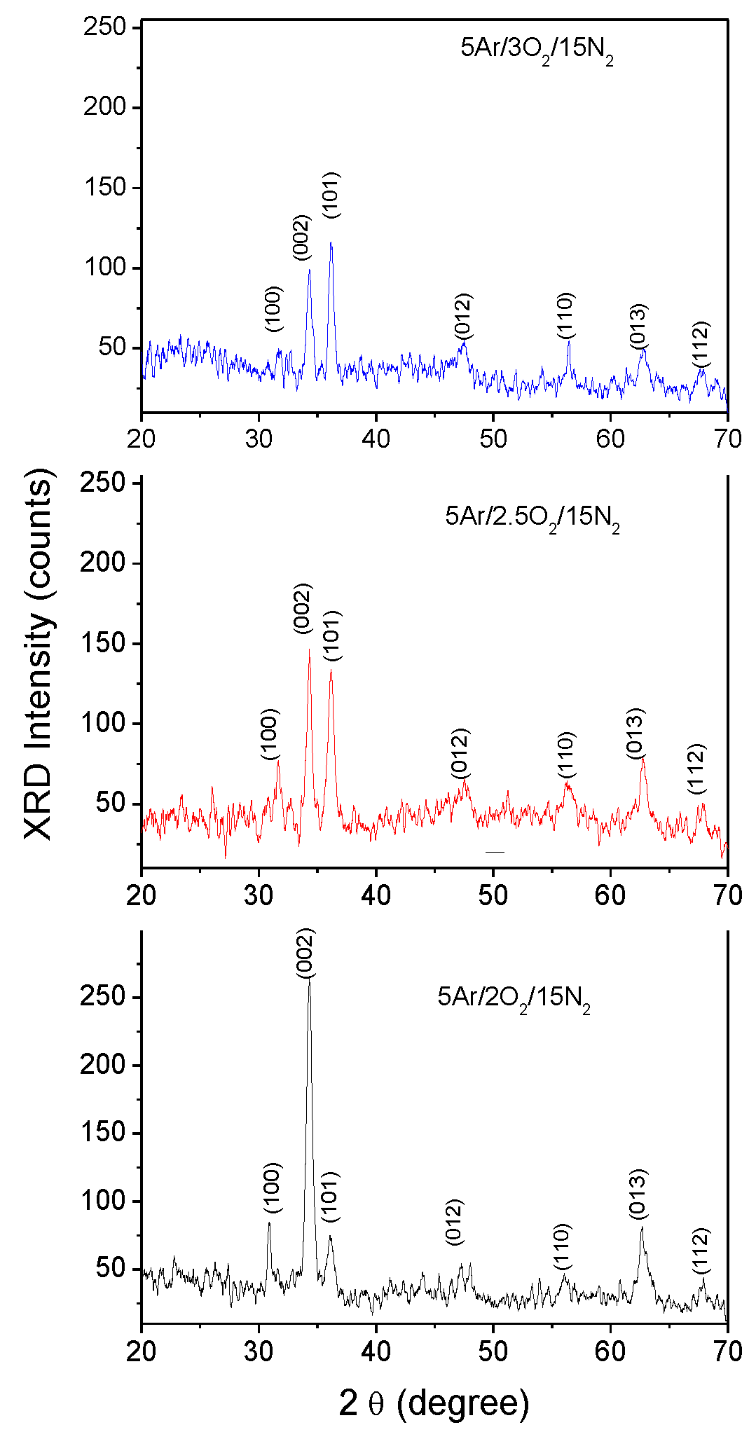
Figure 1. X-ray diffraction patterns of p-type ZnO:Ag,N thin films deposited under a sputtering reactive atmosphere of (a) 5Ar/3O2/15N2, (b) 5Ar/2.5O2/15N2 and (c) 5Ar/2O2/15N2 and annealed after deposition at 400 °C.
Preprints 106043 g001
Figure 2. Raman spectra of p-type ZnO:Ag,N thin films deposited under a sputtering reactive atmosphere of 5Ar/3O2/15N2, 5Ar/2.5O2/15N2, and 5Ar/2O2/15N2 and annealed after deposition at 400 °C.
Preprints 106043 g002
Figure 3. Photoluminescence spectra of p-type ZnO:Ag,N thin films deposited under a sputtering reactive atmosphere of 5Ar/3O2/15N2, 5Ar/2.5O2/15N2, and 5Ar/2O2/15N2 and annealed after deposition at 400 °C.
Preprints 106043 g003
Figure 5. Effect of the impurities on the formation of energy bands for the different single and dual doped p-type zinc oxides compounds.
Preprints 106043 g006
Table 1. Elemental atomic concentration for the p-type ZnO:Ag,N thin films deposited under a tre different sputtering reactive atmospheres and annealed at 400 °C.
Film Gas flow ratio
Ar/O2/N2 (sccm)
Atomic percentage (%)
Zn O N Ag
1-400 5.0/3.0/15.0 36.28 57.54 4.65 1.56
2-400 5.0/2.5/15.0 37.27 58.30 3.78 0.59
3-400 5.0/2.0/15.0 39.56 55.60 3.80 1.04
Table 2. Initial values of the carrier density, mobility and resistivity for the p-type ZnO:Ag,N thin films.
Film Gas flow ratio
Ar/O2/N2 (sccm)
Initial Values
Carrier density (cm-3) Mobility (cm2/V.s) Resistivity (Ω.cm) Type conductivity
1-400 5.0/3.0/15.0 3.290E17 16.05 1.182E-01 p-type
2-400 5.0/2.5/15.0 7.008E17 20.46 4.33E-01 p-type
3-400 5.0/2.0/15.0 3.174E19 22.99 8.555E-03 p-type
Disclaimer/Publisher’s Note: The statements, opinions and data contained in all publications are solely those of the individual author(s) and contributor(s) and not of MDPI and/or the editor(s). MDPI and/or the editor(s) disclaim responsibility for any injury to people or property resulting from any ideas, methods, instructions or products referred to in the content.
Copyright: This open access article is published under a Creative Commons CC BY 4.0 license, which permit the free download, distribution, and reuse, provided that the author and preprint are cited in any reuse.
Prerpints.org logo

Preprints.org is a free preprint server supported by MDPI in Basel, Switzerland.

Subscribe

© 2024 MDPI (Basel, Switzerland) unless otherwise stated