1. Introduction
Graphene, two-dimensional carbon materials, has attracted much interests during two decades since the first discovery because it has unique electrical, optical and physical properties, which can be manipulated in a variety of fundamental research and applications. Graphene, however, has no band gap and its electrical band structure is a semimetal which has a linear energy-momentum dispersion relation [
1]. In order to make a transistor with a graphene for useful memory application, graphene should become semiconducting with a functionalization through electrical, chemical and geometrical manipulation. Meanwhile, several works have reported the formation of band gap in graphene in the concept of symmetry breaking, especially mirror symmetry, which induces a change in band structure. Firstly, Han et al. had reported the band gap tuning in the geometry of nano-ribbon [
2], and the band gap scales with the size of ribbon. On the other hands, defect generation [
3], impurity doping [
4,
5] and applied bias [
6,
7,
8] have induced a band gap opening in graphene. In addition, the boron doping into graphene also reported the tuning of band gap engineering [
5]. Although those reported results are useful and stable for device operation, i.e., more than 0.5 eV for suitable operation of transistor, a more precise and facile control for the band gap formation of the graphene is still demanded to realize room-temperature device applications.
In this study, we report a band gap formation and p-type semiconducting property of graphene doped by electrochemical method on the graphene surface. Among useful electrolytes, KMnO4 is decomposed into K+ + MnO4− by applied bias. Then, manganese-oxide can easily combine with the unsaturated dangling bond on graphene during the doping process, under the optimized applied potential. In other words, the nanoparticle as a form of metal-oxide, manganese dioxide, is adsorbed on the graphene surface. We call this reaction as a doping because the reaction produces a carrier. Furthermore, the amounts of the doping can be adjusted by electric potential. The manganese-oxide nanoparticles adsorbed on the graphene were used as the source of dopants in an electrolyte, which generates the band gap opening and the electronic structure changes
2. Materials and Methods
The graphene film was grown on a Cu foil (Nilaco Corporation, Japan) using a chemical vapor deposition (CVD) system. The reactor was initially evacuated to a base pressure of 2 Torr and then filled with 300 sccm (cubic centimeter per minute) of Ar gas at a pressure of 8 Torr. Subsequently, the copper foil substrate was heated to 950 °C and annealed for 30 min with 30 sccm of H
2 gas. CH
4 (1 sccm) was used as the hydrocarbon source for the growth of graphene. The growth time of graphene was 5 min. The sample was rapidly cooled to room temperature and it was subsequently transferred onto silicon substrate coated with a 300 nm SiO
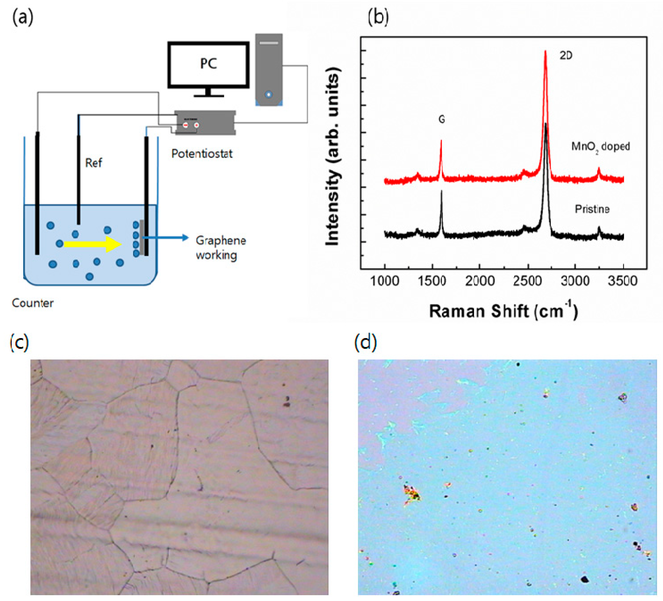
2 layer after etching a Cu film with a spin coating layer with a PMMA, Poly (methyl methacrylate) solution. WPG potentiostats with both a counter electrode of Pt and a reference electrode Ag/AgCl are used for the process of electrochemical doping (
Figure 1(a)). The common glass beaker, as an electrochemical cell, is used for the experiment. The electrolyte solution for the doping is a 0.1 M KMnO
4/DI-water. The working electrode is a graphene thin film connected electrically on Pt wire. The applied potential, optimized for the nanoparticle adsorption, is 1.5 V for 5 min, and MnO
4- ion is simultaneously doped on graphene. Then, the doped film was annealed at 80 °C in a vacuum oven. The electronic structure is investigated by using the x-ray photoelectron spectroscopy (XPS, Versaprobe II ULVAC-PHI). Raman spectra for the graphene films are investigated for the excitation of the wavelength, 514.5 nm at room temperature, using a spectrometer ((Horiba Jobin-Yvon, Oberursel, Germany, HR800UV). The electrical transport, i.e., temperature dependence of conductivity of the doped graphene was measured by using the home-made I-V measurement system composed of a cold head (Sumitomo Heavy Industries, Ltd. RDK-205D) with a He displex and a temperature controller (Lake Shore Cryotronics, Inc. model 331). I-V characteristics of the graphene field effect transistor (FET) doped with manganese-oxide are measured in atmosphere using the Agilent semiconductor parameter analyzer.
3. Results and Discussion
3.1. Optical Microscopy and Raman Spectra
Figure 1 shows the schematic picture of an electrochemical doping system, Raman spectroscopy image of monolayer graphene films, optical microscopy image of graphene on a Cu hoil and optical microscopy image of graphene transferred on a Si substrate. The
Figure 1(a) illustrates the doping procedures as is mentioned in experimental section and Raman spectra are shown in the right panel of
Figure 1. Additionally,
Figure 1(c) and (d) show the optical spectroscopy image of graphene on a Cu foil and Si substrate. The image of graphene on a Cu hoil after CVD synthesis showed a polycristalline structure and the optical image and color of the transferred graphene indicates a monolayer graphene. On the other hand, there are three dominant peaks which involve in the G peak at ~1580 cm
-1, the 2D peak at ~2683 cm
-1, and the D peak at ~1352 cm
-1 in Raman spectra. In general, it is well known that the single layer of the graphene has the unique intensity ratio, the 2D peak to G peak (I
2D/I
G) over 2, and the full width at half maximum (FWHM) of the 2D band is almost close to 30 cm
-1 [
9,
10,
11,
12]. The ratio of our pristine sample, single layer, has the I
2D/I
G ratio of 2.5, and the FWHM of 33 cm
-1 at the single Lorentzian 2D band, which indicates the single layer graphene. Furthermore, the Raman spectra of the doped film by manganese-oxide is shown in red in
Figure 1(b). The peculiar property is not shown in Raman signal due to the doping, however, transport properties will be discussed in device characteristics and temperature dependent conductivity.
3.2. XPS Spectra
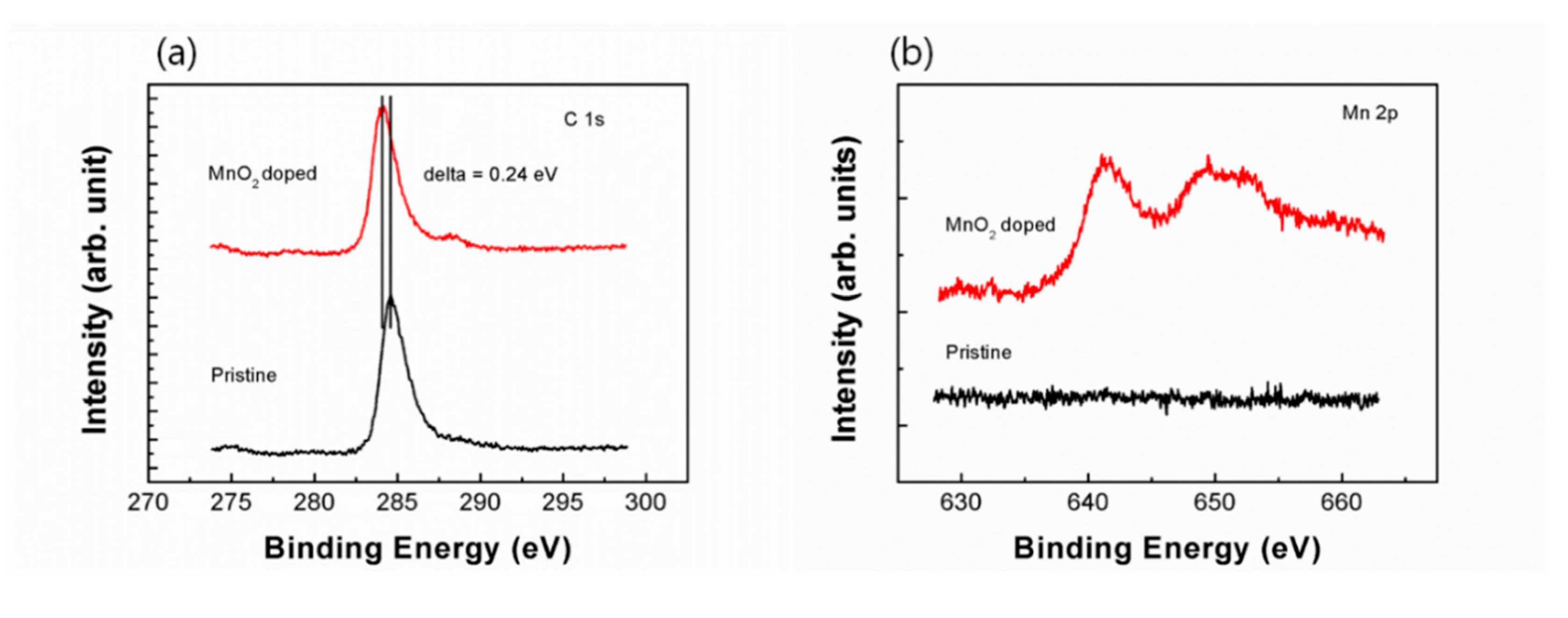
The XPS analysis of the pristine and the doped graphene are shown in
Figure 2. The carbon 1s spectra, peak position at 284.5 eV for the pristine graphene without doping manganese-oxide is very close to the original value for the pure sp
2 C–C bonding as can be seen in the highly oriented pyrolytic graphite (HOPG), and this indicates that the carbon atoms of the graphene are almost exclusively sp
2 hybridized in the pristine graphene [
13]. The downshift of the carbon core level of 0.24 eV in the binding energy of graphene doped at 1.5 V by manganese-oxide evidences p-type doping with the Fermi level change as the MnO
4− ion concentration increases. The manganese Mn 2p core level spectra of graphene which is doped at 1.5 V, depicted in Figure. 2(b) indicates a prominent difference between two spectra. The pristine sample has no manganese peak expectedly over all scan ranges, whereas the doped sample, red spectra show clearly the existence of manganese core level of Mn 2p. This means that the doped graphene has the manganese atoms to bonded to carbon lattice, which make an electronic structure to be semiconducting by breaking the lattice symmetry. So, electrical and thermal properties of the doped graphene will be appeared.
3.3. Device Characteristics
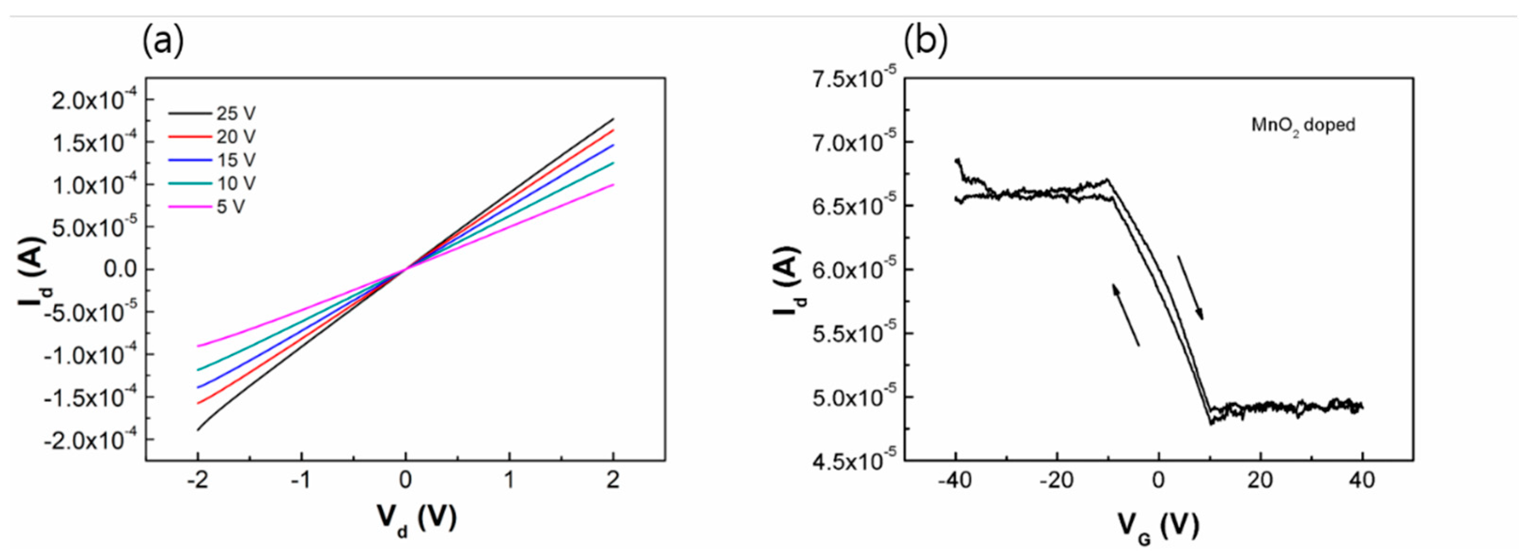
Figure 3 shows the device outputs, I-V characteristics of the graphene FET doped with manganese-oxide. We fabricated a back-gate FET as a channel layer of the manganese-oxide doped graphene. The p-type Si substrate doped with boron is used for the back gate electrode, and a 300-nm-thick dielectric layer, silicon dioxide (SiO
2) is coated on substrate as a gate insulator. A 50-nm gold layer is deposited to make the electrodes of source and drain on the graphene film by e-beam evaporation method. The channel length is the 100 μm, and the channel width is the 10 μm. I-V curves of the graphene FET device are measured in atmosphere at room temperature. From
Figure 3(a), we see the typical I-V characteristics, linearly increasing of FET as the gate voltage increases. In addition,
Figure 3(b) reveals that the graphene FET has a p-type property and has an on/off ratio, 1.3, which can be identified from the transfer curve of
Figure 3(b). During the process of the electrochemical doping, the charge transfer is occurred between the graphene and the manganese-oxide. The drain current (I
d) of the doped graphene FET apparently increases with increasing negative gate bias as a p-type behavior. The field effect mobility of the devices is determined by calculating the linear region using the equation, µ = (L/WC
oxV
d)(ΔI
d/ΔV
g); where L is the channel length and W, the width, respectively, and C
ox is the gate capacitance of the 300nm-thick SiO
2. The field effect mobility is approximately 1856 cm
2V
-1s
-1 for the manganese-oxide doped graphene. Therefore, the graphene doped by manganese-oxide can play a role of p-type transistor with a switchable on-off ratio, semiconducting properties.
3.4. Transport
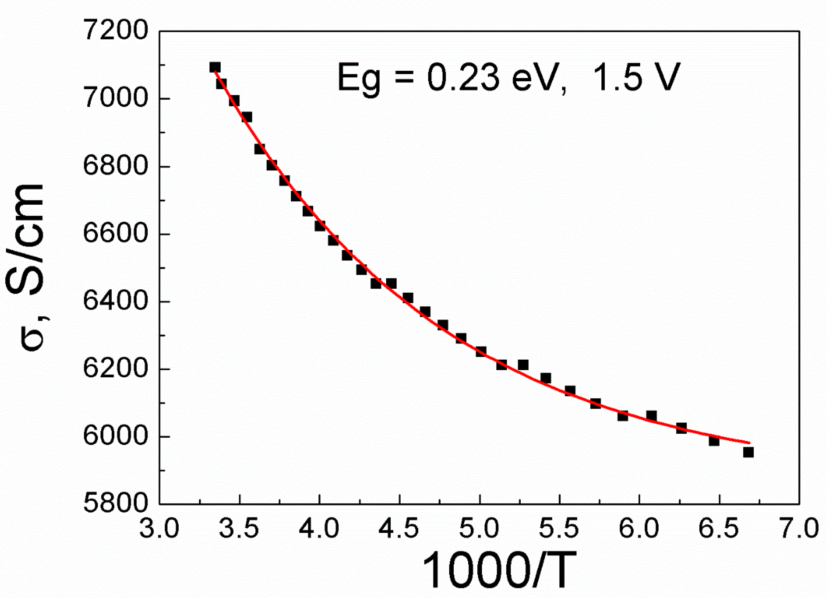
Figure 4 indicates that the results of temperature-dependent conductivity of the doped graphene show a band gap opening in the doped graphene as found in the temperature region ranging from 150 to 300 K. It indicates a typical semiconductor behavior, and is fitted by exponential function [
14,
15]. The semiconducting behavior is attributed to the sublattice symmetry breaking of graphene caused by bonding of manganese-oxide. According to the theoretical work, the adsorbed molecules on the graphene behaves like defects and the manganese-oxide nanoparticles break the symmetry of the sublattice. As a result, it make a band gap in the graphene band structure [
16]. As reported from the previous work, the temperature-dependence of conductivity of graphene can be well analyzed by the variable range hopping (VRH) mechanism at very low temperatures. As shown in Ref 17. VRH conduction is dominant below 50 K, and the effects of the nearest-neighbor hopping (NNH) follows a conductivity equation, σ ∝ exp(−T
0/T) [
17]. However, the main transport mechanism is like that the thermally activated (TA) conduction at high temperature range, over 100K is well explained by theoretical fitting. The TA model can be applied as: σ = σ
0exp (- E
g/2k
BT) for the regions of high temperature over 100 K [
14,
15]. We obtained that the observed band gap of the manganese-oxide doped graphene from conductivity versus temperature is shown to be 0.23 eV. We think that the highly effective value of a band gap for room-temperature device operation is needed further study in future.
4. Conclusions
We have studied that the doped graphene by manganese-oxide using an electrochemical method produce a metal-semiconductor transition in graphene. Semiconducting property was well observed in the monolayer graphene field effect transistor and temperature dependence of transport. The transport measurements indicate that the doped film is p-type and its band gap is 0.23 eV from the conductivity-temperature fitting. The semiconducting properties of manganese-oxide doped graphene is appeared due to the formation of manganese-oxide nanoparticle on the surface of graphene. This work suggests that the semiconducting property of the manganese-oxide doped graphene can be utilized in new research area on electronic devices in the future.
Author Contributions
C.-S. Park: Conceptualization, Formal analysis, Original Manuscript Writing, Y. H. Kwon: Investigation, Measurement, Writing. H. Kim: Data curation. Analysis. Writing, D.Y. Kim: Writing—review & editing, Funding acquisition. All authors have read and agreed to the published version of the manuscript.
Funding
This research was supported by Basic Science Research Program through the National Research Foundation of Korea (NRF) funded by the Ministry of Education (2016R1A6A1A03012877).
Data Availability Statement
Data are contained within the article
Conflicts of Interest
The authors declare no conflict of interest.
References
- Novoselov, K. S.; Geim, A. K.; Morozov, S. V.; Jiang, D.; Katsnelson, M. I.; Grigorieva, I. V.; Dubonos, S. V.; Firsov, A. A. Two-dimensional gas of massless Dirac fermions in graphene, Nature 2005, 438, 197. [CrossRef]
- Han, M. Y.; Ozyilmaz, B.; Zhang, Y; Kim, P. Energy band-gap engineering of graphene nanoribbons, Phys. Rev. Lett. 2007, 98, 206805. [CrossRef]
- Dong, X.; Shi, Y.; Zhao, Y.; Chen, D.; Ye, J.; Yao, Y.; Gao, F.; Ni, Z.; Yu, T.; Shen, Z.; Huang, Y.; Chen, P.; Li, L. -J. Symmetry breaking of graphene monolayers by molecular decoration, Phys. Rev. Lett. 2009, 102, 135501. [CrossRef]
- Ohta, T.; Bostwick, A.; Seyller, T.; Horn, K.; Rotenberg, E. Controlling the electronic structure of bilayer graphene, Science 2006, 313, 951. [CrossRef]
- Tang, Y. -B.; Yin, L. -C.; Yang, Y.; Bo, X. -H.; Cao, Y. -L.; Wang, H. -E.; Zhang, W. -J.; Bello, I.; Lee, S. -T.; Cheng, H. -M.; Lee, C. -S. Tunable band gaps and p-type transport properties of Boron-doped graphenes by controllable ion doping using reactive microwave plasma, ACS Nano 2012, 6, 1970. [CrossRef]
- Rudberg, E.; Salek, P.; Luo, Y. Nonlocal exchange interaction removes half-metallicity in graphene nanoribbons, Nano Lett. 2007, 7, 2211. [CrossRef]
- Son, Y.-W.; Cohen, M. L.; Louie, S. G. Half-metallic graphene nanoribbons, Nature 2006, 444, 347. [CrossRef]
- Zhang, Y.; Tang, T. -T.; Girit, C.; Hao, Z.; Martin, M. C.; Zettl, A.; Crommie, M. F.; Shen, R.; Wang, F. Direct observation of a widely tunable bandgap in bilayer graphene, Nature 2009, 459, 820. [CrossRef]
- Ferrari, A. C.; Meyer, J. C.; Scardaci, V.; Casiraghi, C.; Lazzeri, M.; Mauri, F.; Piscanec, S.; Jiang, D.; Novoselov, K. S.; Roth, S.; Geim, A. K. Raman spectrum of graphene and graphene Layers, Phys. Rev. Lett. 2006, 97, 187401. [CrossRef]
- Li, X.; Cai, W.; An, J.; Kim, S.; Nah, J.; Yang, D.; Piner, R.; Velamakanni, A.; Jung, I.; Tutuc, E.; Banerjee, S.; Colombo, L.; Ruoff, R. S. Large-area synthesis of high-quality and uniform graphene films on copper foils, Science 2009, 324, 1312. [CrossRef]
- Ni, Z. H.; Wang, H. M.; Kasim, J.; Fan, H. M.; Yu, T.; Wu, Y. H.; Feng, Y. P.; Shen, Z. H. Graphene thickness determination using reflection and contrast spectroscopy, Nano Lett. 2007, 7, 2758. [CrossRef]
- Malard, L. M.; Pimenta, M. A.; Dresselhaus, G.; Dresselhaus, M. S. Raman spectroscopy in graphene, Phys. Rep. 2009, 473, 51. [CrossRef]
- Maldonado, S.; Morin, S.; Stevenson, K. J. Structure, composition, and chemical reactivity of carbon nanotubes by selective nitrogen doping, Carbon 2006, 44, 1429. [CrossRef]
- Miyazaki, H.; Tsukagoshi, K.; Kanda, A.; Otani, M.; Okada, S. Influence of disorder on conductance in bilayer graphene under perpendicular electric field, Nano Lett. 2010, 10, 3888. [CrossRef]
- Park, C. -S.; Zhao, Y.; Shon, Y.; Yoon, I. T.; Lee, C. J.; Song, J. D.; Lee, H.; Kim, E. K. Properties of room-temperature ferromagnetic semiconductor in manganese-doped bilayer graphene by chemical vapor deposition, J. Mater. Chem. C 2015, 3, 4235. [CrossRef]
- Cretu, O.; Krasheninnikov, A. V.; Rodriguez-Manzo, J. A.; Sun, L.; Nieminen, R. M.; Banhart, F. Migration and localization of metal atoms on strained graphene, Phys. Rev. Lett. 2010, 105, 196102. [CrossRef]
- Park, C. -S. Disorder induced transition of electrical properties of graphene by thermal annealing, Results in Physics. 2018, 9, 1534. [CrossRef]
|
Disclaimer/Publisher’s Note: The statements, opinions and data contained in all publications are solely those of the individual author(s) and contributor(s) and not of MDPI and/or the editor(s). MDPI and/or the editor(s) disclaim responsibility for any injury to people or property resulting from any ideas, methods, instructions or products referred to in the content. |
© 2024 by the authors. Licensee MDPI, Basel, Switzerland. This article is an open access article distributed under the terms and conditions of the Creative Commons Attribution (CC BY) license (http://creativecommons.org/licenses/by/4.0/).


