1. Introduction
As PIC maturity continues to increase leading to wide acceptability in industries and commercial, the complexity of PIC has also increased due to large number of components on a single chip [
1,
2]. Demonstrations with more than 1500 components on a single chip have been achieved and more is expected [
1]. The success of PIC can be attributed to the possibility of large scale production in Silicon photonics at reduced footprint, low component-to-component losses, low power consumption and low overall packaging cost [
3]. This has allowed PIC to be used in application specific photonic integrated circuits (ASPIC), which plays a role in data/tele communications, medical applications and bio sensing and even more recently in transportation such as LIDAR [
4,
5]. Such application specific designs require painstaking efforts, long time and high cost to achieve result and the design cannot be transformed or used for other applications except the specific purposes they are designed for [
6]. In some cases, the design may fail to meet the initial objective, which implies that the process has to be repeated and the cost of production will be increased [
6].
The advent of programmable photonics introduces a generic template that can be exploited to implement a variety of functionality through software [
7]. Just like we have field programmable gateway arrays (FPGA) in electronics which can be reconfigured to meet specific use case of customers, programmable photonics introduce such generic functionality known as field programmable photonic gateway arrays (FPPGA) for widespread PIC design in optical communications [
8]. These FPPGAs are electronically reconfigurable basic elements that allow flexible configuration of a set of passive devices in order to mime several circuits without undergoing the long-time conventional fabrication circle [
6,
9,
10]. Most of the FPPGA architectures are based on cascaded Mach Zehnder modulator (MZM) structures in various shapes and dimensions [
11,
12].
In this paper, a pulse amplitude modulation four level (PAM-4) transmitter based on oDAC will be analyzed using the hexagonal FPPGA mesh developed by iPronics [
9,
12]. This type of transmitter is an alternative approach to replace a power hungry electrical digital to analog converter (eDAC) that is required in the conventional PAM-4 signal generation [
13,
14]. The oDAC devices are based on digital modulators and passive devices such as couplers and splitters [
13]. Therefore, as a result of light-interfering nature of such devices, precision is not guaranteed due to slight deviation during fabrication which may result in performance degradation and low-yield [
15,
16]. The programmability and reconfigurability of the iPronics FPPGA as reported in [
9,
10] are applied to oDAC PAM-4 transmitter in order to investigate its potential fabrication tolerances and predict production yield, as a continuation of our work in [
17].
Monte-Carlo emulation of 1000 chips to mime oDAC PAM-4 transmitter was carried out experimentally in iPronics programmable grid considering different splitter values due to fabrication errors. We then offline statistically estimated the SER performance of the devices, which we used to predict the failed and passed chips. Our aim is to demonstrate the potential of the methodology to evaluate the viability of a certain fabrication technique to meet the required yield.
2. Proposed Model
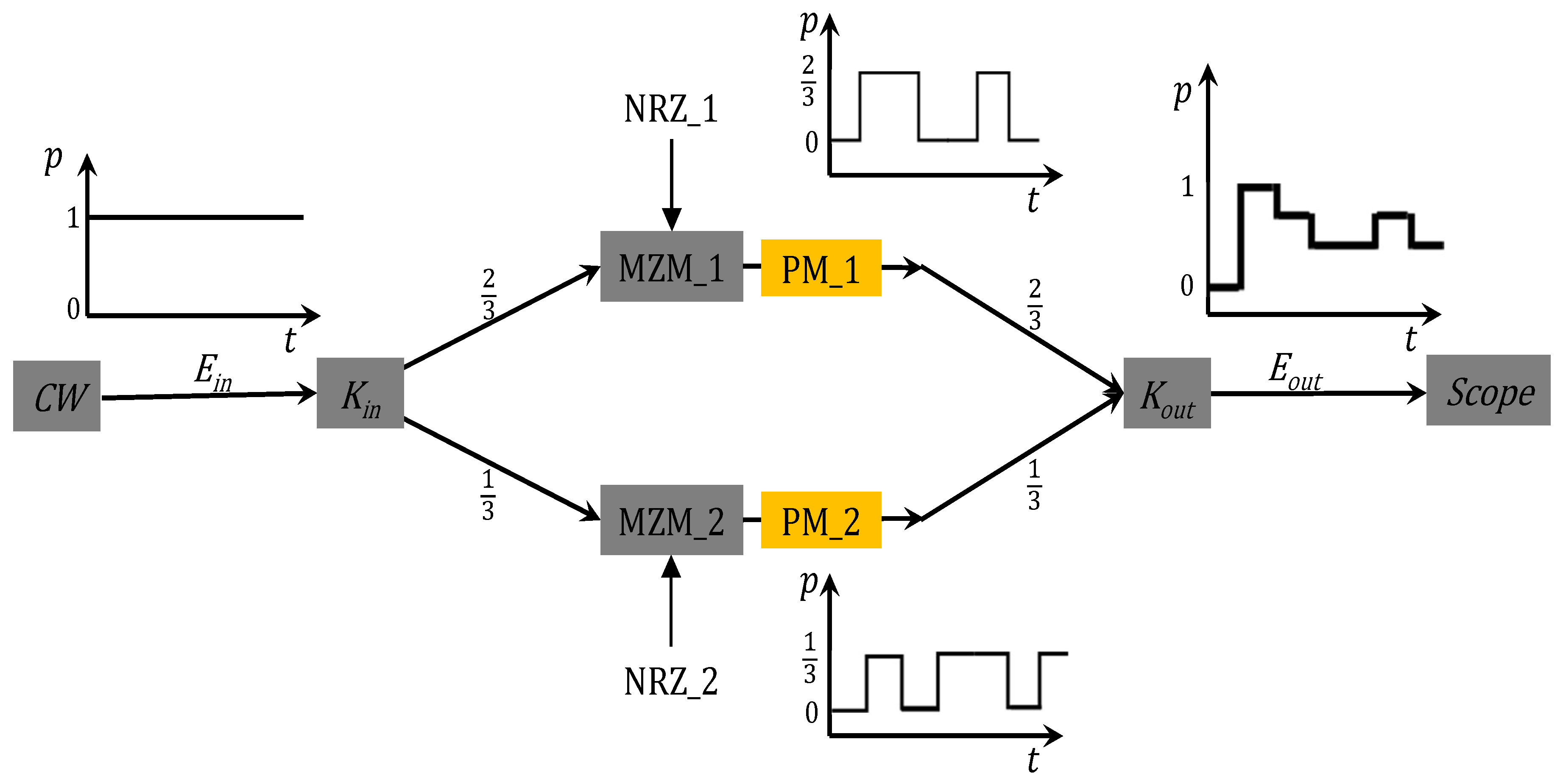
An oDAC PAM-4 transmitter is presented in
Figure 1 where signal from a continuous wave (CW) laser is split into the two arms of the device through an input coupler with
and then recombined through an output coupler with
. The non-return-to-zero (NRZ) electrical signals (
and
) which act as most significant bit (MSB) and least significant bit (LSB) are applied to drive the modulators as shown on
Figure 1.
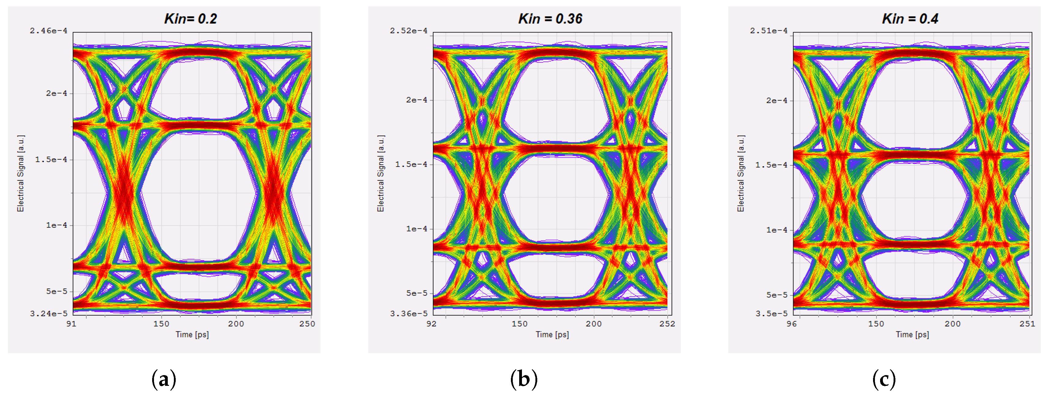
Due to the sensitive nature of interferometers, imprecision in the implementation of this type of device can reduce performance during signal detection. For instance, eye diagrams at different values of
are presented in
Figure 2 (a), (b) and (c). This is a challenge that requires further investigation.
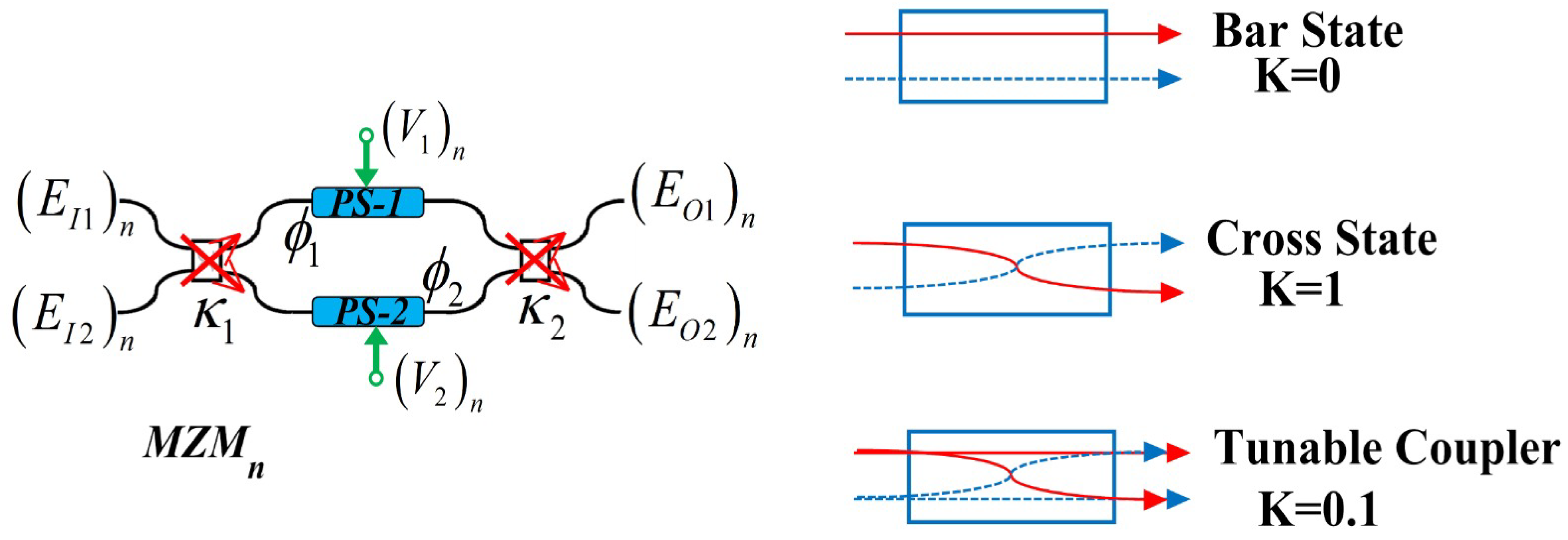
To model this effect, one FPPGA device developed by iPronics which comprises a set of MZMs or programmable unit core (PUC)s which are hexagonally connected via replicated geometric is used. Each PUC from the arrays is itself a MZM as shown in
Figure 3 which can be configured as bar state with
= 0, cross state with
= 1, and as tunable with
= any value between 0 and 1.
The mathematical expression of the output signal of a typical PUC/MZM as shown in
Figure 3 (a) can be expressed as
where
and
are the applied voltages to tune the phase shifter (PS) in order to create
and
phase changes,
and
, PUC input and output coupling coefficients,
, the half-wave voltage and
.
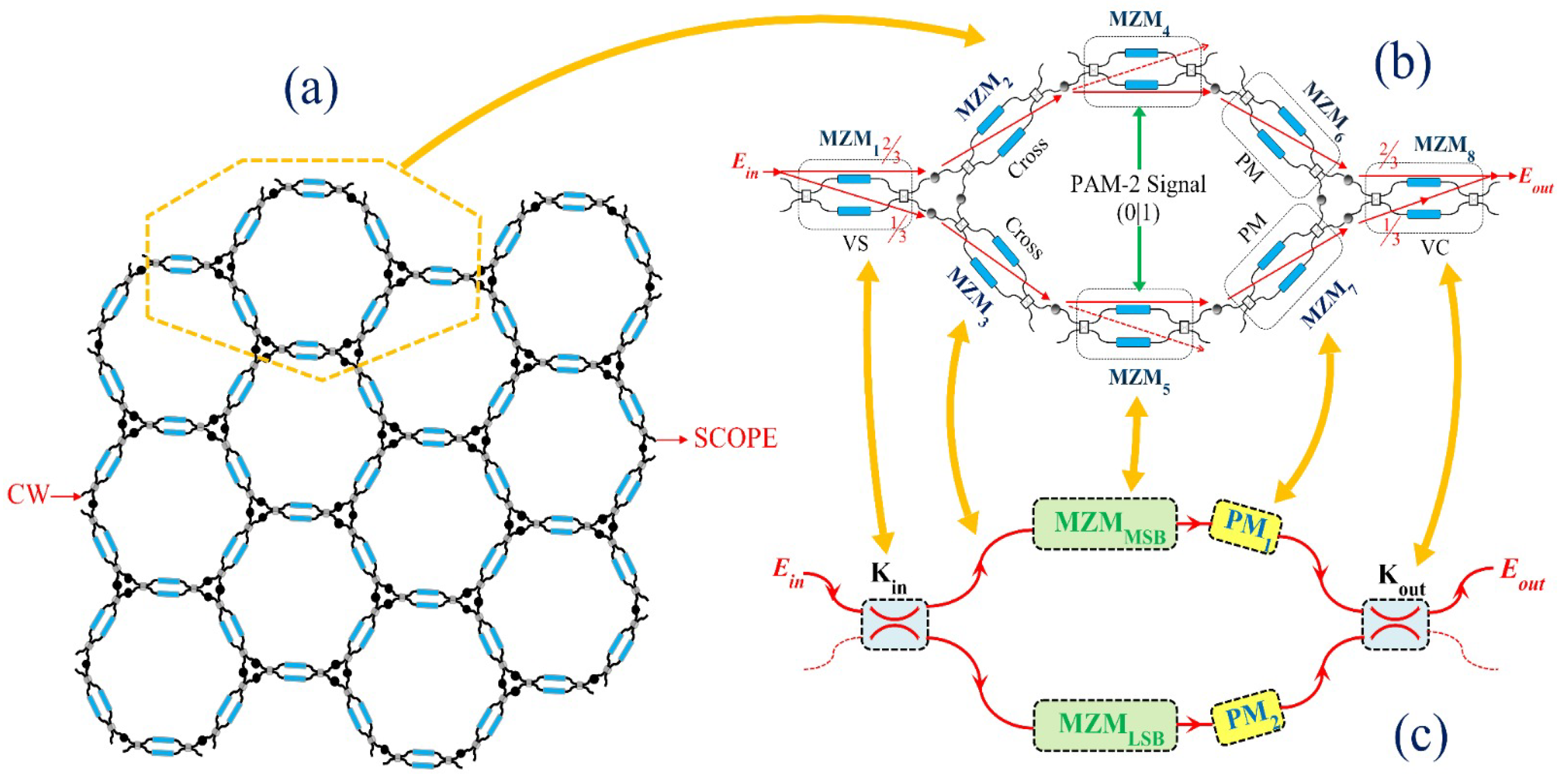
Hexagonal arrays of the PUCs is shown in
Figure 4 (a) and it can be electrically tuned to provide functionalities such as filtering, optical interconnects and several other optical functionalities.
Furthermore, our proposed model
Figure 4 (b) and (c), developed from the PUC arrays in
Figure 4 (a), comprises two MZM acting as amplitude modulator (AM) (
and
) which are arranged in parallel to form the two arms just as another major MZM circuit. Light from a CW laser can then be split into the two arms of the outer MZMs via an input optical splitter (which itself is a MZM) by setting its
to 0.36 as recommended in [
14].
In addition, phase modulator (PM)s mimed as and are placed immediately after each AM before the two signals are combined through an optical combiner with = 0.5. By coarse adjustment of the phase of either or , resulting in phase adjustment, we can improve the PAM-4 to be equidistant.
To generate a PAM-4 signal using the proposed device, two NRZ digital signals are applied to drive the two AM where each driving implies a 1-bit modulation gate as shown on
Figure 4 (b) and (c). The constellation levels of the PAM-4 signal are set to
following the oDAC design specification in [
14].
Moreover, by making the input PUC (
in
Figure 4 (b)) that mimes
a random variable with Gaussian distribution, which implies that
=
+
, where
is the fabrication variance, we can mime the fabrication tolerance of the device. So, a Monte-Carlo emulation of the device is then carried out. For the sake of time, only 1000 devices iterations are considered. At first, the simulation is conducted for a perfect passive coupling condition with the
set to 0%. Then,
is further varied from 2% to 12%. As it is expected, the coupling ratio of a passive device cannot surpass 1, we opted to mime the effect of coupling resulting from the sinusoidal behaviour of MZM leading to folded "1’s" and "0’s".
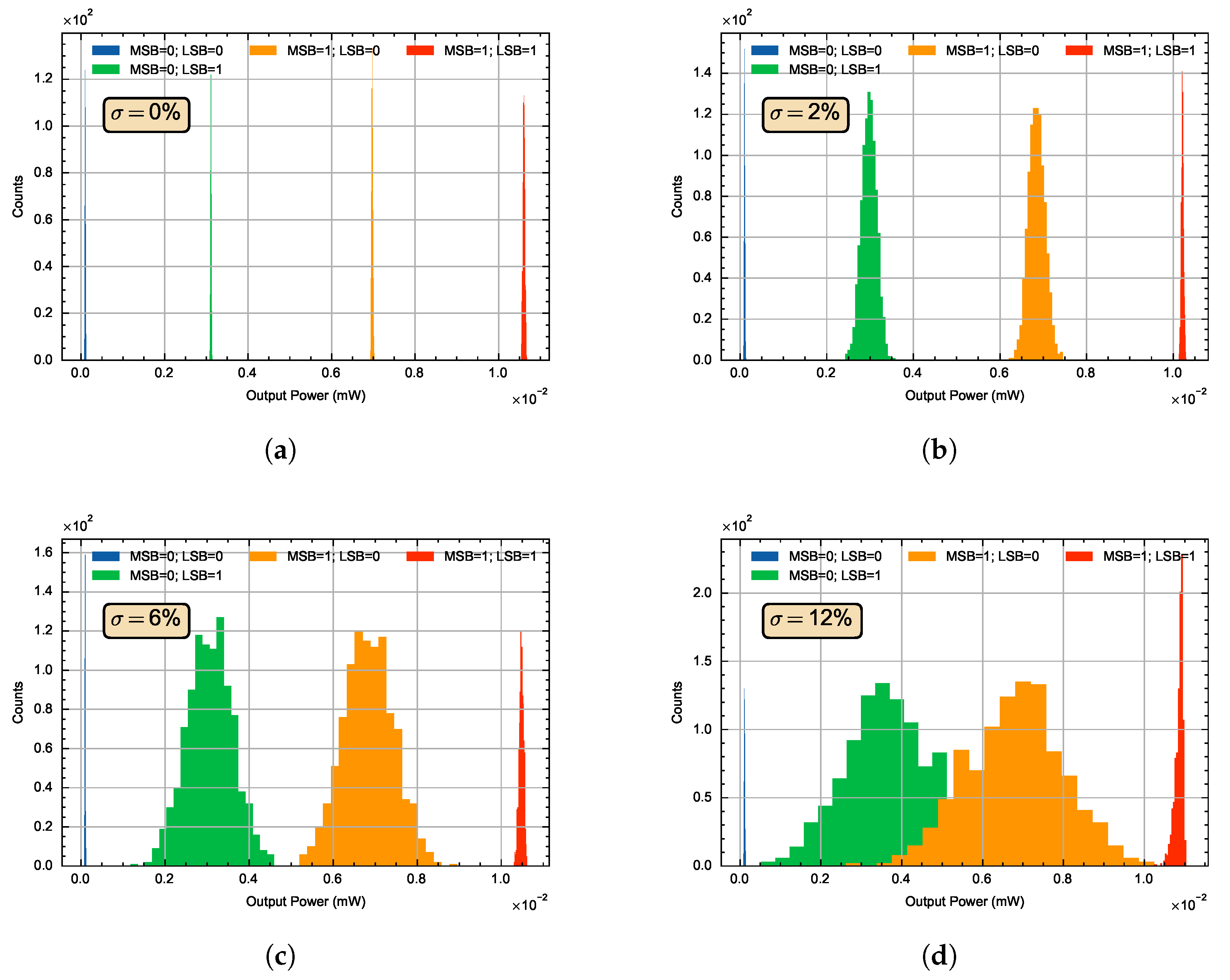
Histogram of the Gaussian profile of the 1000 chips for a perfect passive coupler is presented in
Figure 5(a) while histograms of increased
from 2-12% are presented in
Figure 5(b),
Figure 5(c) and
Figure 5(d) respectively. No sign of imbalance is observed on
Figure 5 as expected since no error is added in this case. From the results in
Figure 5(b),
Figure 5(c) and
Figure 5(d),
remains unchanged despite increased
since this level implies an absence of light. However, increased
significantly impaired
and
due to overlapping which may result in decision error.
maintains improvement when compared with
and
. This is because,
has the highest signal-to-noise ratio since the highest signal power occurred at this level. Nevertheless, impact of increased
can be seen to cause
to fold back towards
.
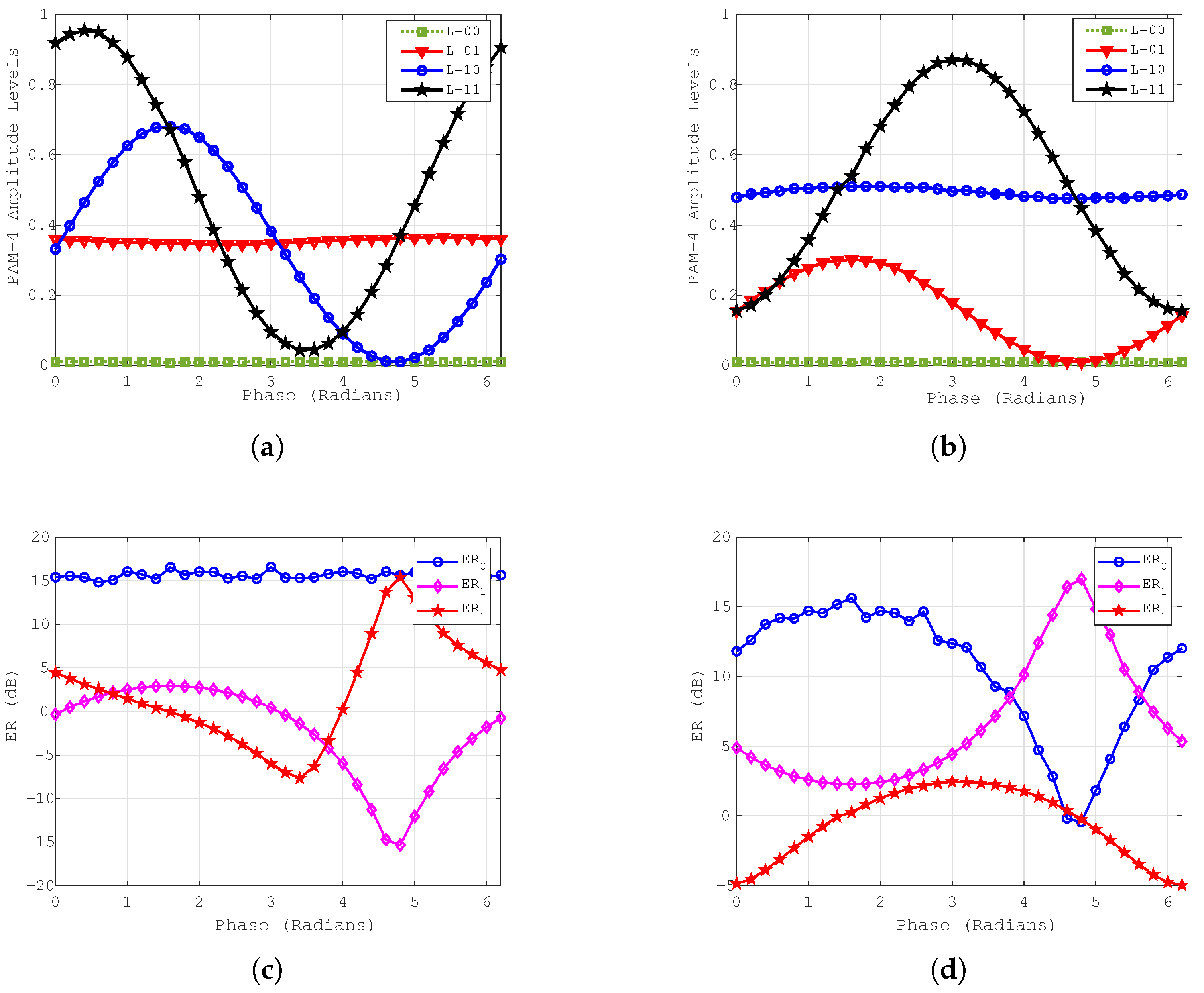
Next, we have optimized to ensure equidistant of amplitude levels of our PAM-4 signal. As the maximum phase shift cannot exceed
, the phases of both PMs (
and
) are swept from 0 to
radians. Variation of the amplitude levels of the oDAC-PAM-4 transmitter’s against phase are obtained and presented in
Figure 6(b) and
Figure 6(a) for
and
as in
Figure 4 (c), showing the distribution of signal amplitude against phase. ER of the PAM-4 eyes against varying phase of
and
are also presented in
Figure 6(c) and
Figure 6(d) showing how phase variation impact the signal’s extinction ratio (ER). We have set the phase of
to 2.4 radians for further analysis conducted on the oDAC-PAM-4 transmitter in this study.
2.1. Data Extraction and Analysis
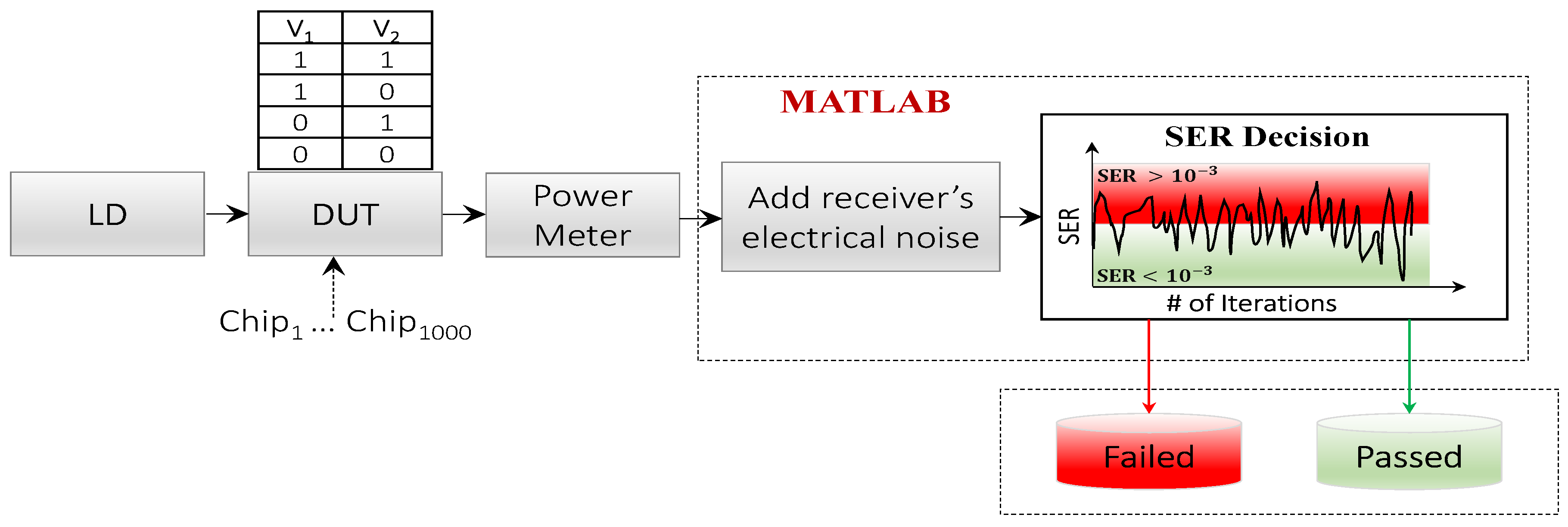
The procedure for data extraction and analysis is presented in
Figure 7. Since the machine can be controlled using software, the process in
Figure 7 follows repeated iterations to mime 1000 oDAC PAM-4 transmitters. Specifically, while varying the value of
in the devices, the signal levels of each of the transmitters are extracted for offline processing.
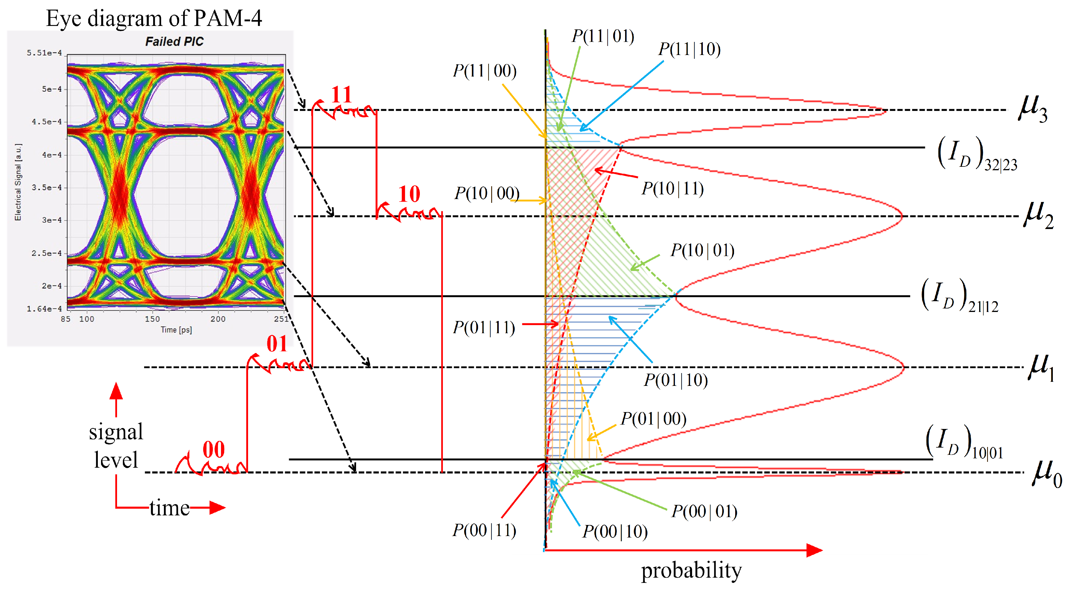
A sketch of the decision circuit showing waveform of bits fluctuation across the four levels of the PAM-4 signal is presented in
Figure A1 in
Appendix A where
is the probability of deciding signal
when signal
is received and
, the Gaussian pulse of the PAM-4 signal levels.
The generalized analytical expression for estimating SER of a PAM-4 signal based on the schematic in
Figure A1 is giving by Equation (
A2) in
Appendix B.
Therefore, solving for all the
in
Figure A1 as presented in Equation (
A2) using Equation (
A4), we obtained Eq
A5 in
Appendix C.
The
in
Appendix B and
Appendix C is the receiver’s electrical noise which is estimated as the sum of thermal and short noise for a typical 10 GHz PIN receiver following the expression in [
18] and it is assumed constant across the four PAM-4 levels. We have further assumed a typical detection of a 10 Gb/s signal at 1550 nm with a receiver’s sensitivity of
dBm at SER =
to adjust the receiver’s noise. In addition to this, the P2P power level of the signal from the machine is normalized to increase the impact of signal noise before detection. The SER bench-mark of
is used to determine the failed or passed chips as clearly illustrated in
Figure 7.
3. Results and Discussion
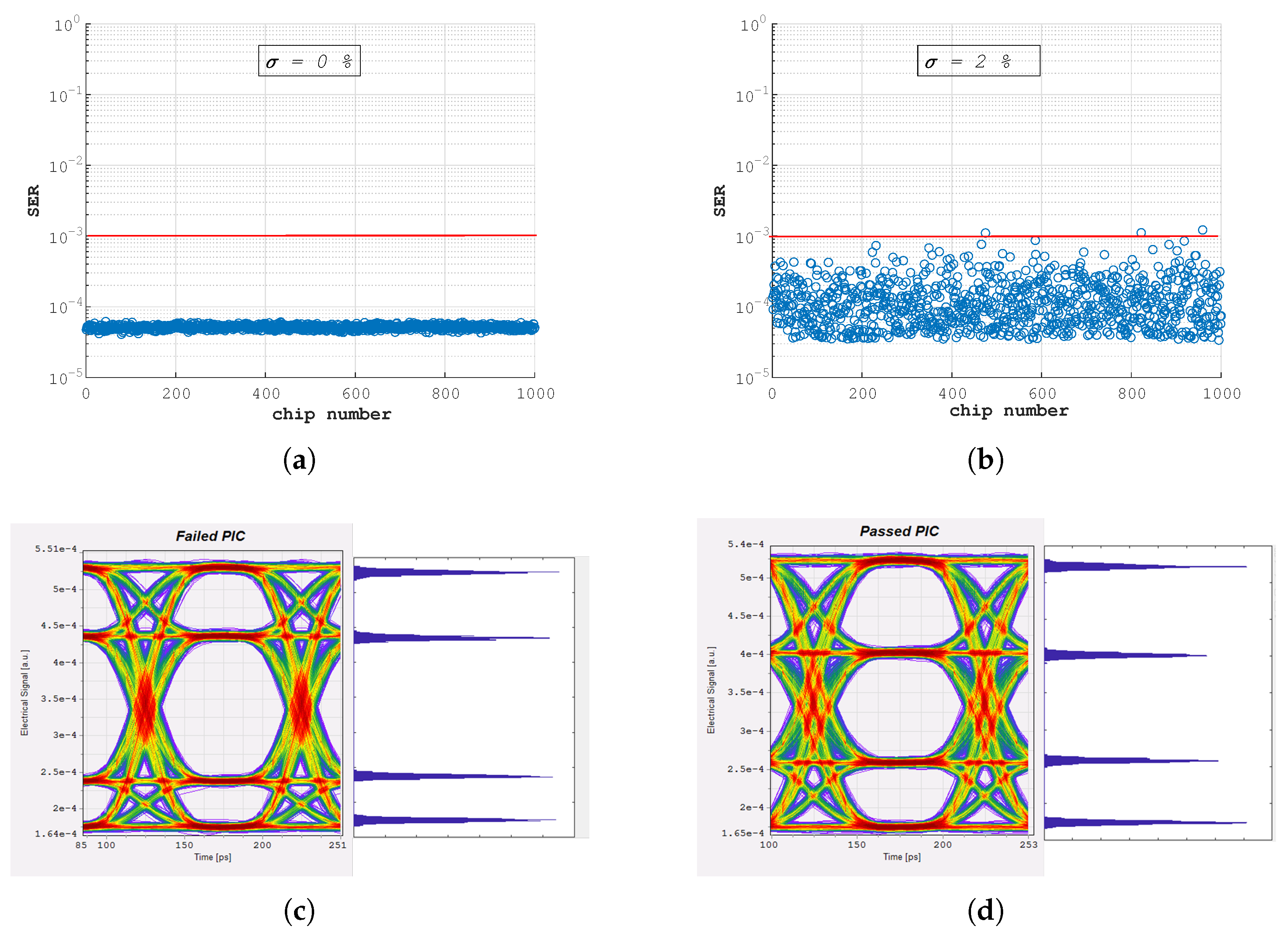
The graphs of SER versus chip iteration when
= 0 and when
= 2 % are presented in
Figure 8(a) and
Figure 8(b). With light control as expected, the total 1000 iterated PIC passed the SER threshold as shown in
Figure 8(a). When
is increased to 2 %, only 3 chips out of 1000 mimed was seen to have failed while the rest passed the SER threshold we have set which implies high tolerance due to less deviation from coupling condition.
For further analysis of the results when
= 2 % , PAM-4 amplitudes levels of one PIC from the failed and passed categories are extracted and simulated to obtain the PAM-4 eye diagrams of the failed and passed PIC as shown in
Figure 8(c) and
Figure 8(d). From the eye diagram of the failed PIC in
Figure 8(c), it can be observed that the amplitude levels of the signal are not equidistant which resulted in error detection. Unlike the passed PIC with the eye diagram in
Figure 8(d), an improved signal equidistant level is observed and as such, the detection is accomplished with less error at the receiver.
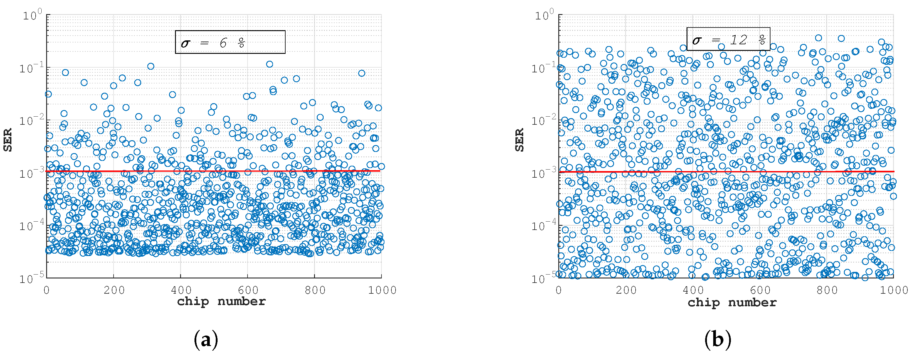
Moreover, by increasing the impact of
from 6 % to 12 %, it is observed that the levels 10 and 01 overlapping increases. As a result of this, the numbers of failed PICs increase, which implies low yield. Looking at the result of
= 12 % in
Figure 9(b) for instance, close to 50 % of the PIC failed due to high spread of levels 01 and 10 as clearly shown on the histogram in
Figure 5(d), which translates to high loss in production scenario.
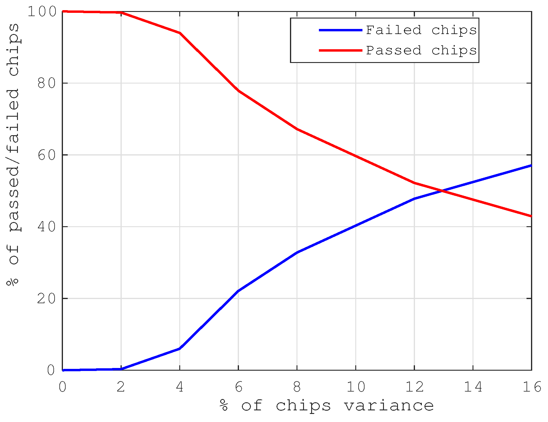
In addition, the graph in
Figure 10 summarizes the percentage of failed and passed chips against all instances of
we have tested, which simplified our
findings. The linear behaviour of the number of both passed and failed chips in the figure can explain what would be expected in fabrication scenario and this serve as a predictive template to analysis any passive device. Furthermore, the graph also reveals that such oDAC based PAM-4 transmitter is sensitive to component deviations resulting from variations in the passives.
4. Conclusions
In this paper, we have presented a hybrid model to study the effects of fabrication tolerance resulting from passive variation in PIC based devices. Using the flexibility of FPPGA, an oDAC-based PAM-4 telecommunication transmitter was mimed and with passive variances ranging from 0...12 % while mimicking the production of 1000 components. Monte-Carlo emulation of the device is carried out to predict the production yield at given instances of passive variation. While bench-marking the SER to , the number of failed and passed PIC have been determined at every instance of passive variances we have tested. These findings enable robust designs which consider critically the sensitive effect of passive variability on designed components and can be formulated into new design rules .
Author Contributions
A. E A: Writing-original draft, Visualization, Conceptualization, Methodology, Investigation, A. T: Visualization, Conceptualization, Supervision, Funding Acquisition, M. L: Supervision, Review, J. S: Investigation, Software, Methodology, T.C: Review, Visualization, Methodology, Investigation F.R: Software, Review, Visualization. All authors have read and agreed to the published version of the manuscript.
Funding
This work is supported by the European Regional Development Fund (FEDER), through the Competitiveness and Internationalization Operational Program (COMPETE 2020) of the Portugal 2020 framework [Project POWER with Nr. 070365 (POCI-01-0247-FEDER- 070365)]. The work is also supported by the European Commission through the HORIZON-JU-SNS-2022 FLEX-SCALE project with Grant Agreement number 101096909.
Institutional Review Board Statement
Not applicable.
Informed Consent Statement
Not applicable.
Data Availability Statement
Not applicable.
Conflicts of Interest
The authors declare no conflict of interest.
Abbreviations
| AM |
amplitude modulator |
| ASPIC |
application specific photonic integrated circuits |
| CW |
continuous wave |
| eDAC |
electrical digital to analog converter |
| ER |
extinction ratio |
| FPGA |
field programmable gateway arrays |
| FPPGA |
field programmable photonic gateway arrays |
|
input coupling factor |
|
output coupling factor |
| LSB |
least significant bit |
| NRZ |
non-return-to-zero |
| MSB |
most significant bit |
| MZM |
Mach Zehnder modulator |
| oDAC |
optical digital to analog converter |
| PAM-4 |
pulse amplitude modulator level four |
| PAM-8 |
pulse amplitude modulator level eight |
| PAM-16 |
pulse amplitude modulator level sixteen |
| PIC |
Photonic integrated circuits |
| PUC |
programmable unit cell |
| PM |
phase modulator |
| PS |
phase shifter |
| PUC |
programmable unit core |
| QAM |
quadrature amplitude modulation |
| SER |
symbol error rate |
Appendix A
Probability density of the four PAM levels are the combination of four Gaussian functions and can be written from generalized Gaussian probability density function as [
19,
20],
Figure A1.
PAM-4 signal waveform showing the signal levels and equivalent Gaussian probability densities of the four levels. Inset is an eye diagram of a simulated 10 Gbps hybrid PAM-4 signal.
Figure A1.
PAM-4 signal waveform showing the signal levels and equivalent Gaussian probability densities of the four levels. Inset is an eye diagram of a simulated 10 Gbps hybrid PAM-4 signal.
Appendix B
This equation can be summarized as
where
can be expressed as
where
and
are the mean and standard deviation of
Gaussian level of the PAM-4 signal.
is the probability of receiving signal level
which is equally possible. In addition, depending on the noise contribution due to signal impairment, there is probability that signal
will constitute an error to symbol
across the four Gaussian pulses in
Figure A1.
is the complimentary error function and
is the threshold values of the signal level
and
. Whenever signal detection is done above the threshold, higher logical state is considered and vice versa.
Appendix C
Some of the
cancelled out in Equation (
A5) and the final expression to estimate the SER of the oDAC PAM-4 is giving by
References
- Smit, M.; Williams, K.; Tol, J.v.d. 1.3 Integration of Photonics and Electronics. 2019 IEEE International Solid- State Circuits Conference - (ISSCC), 2019, pp. 29–34. [CrossRef]
- Bogaerts, W.; Rahim, A. Programmable photonics: An opportunity for an accessible large-volume PIC ecosystem. IEEE Journal of Selected Topics in Quantum Electronics 2020, 26, 1–17. [Google Scholar] [CrossRef]
- Dai, D.; Bauters, J.; Bowers, J.E. Passive technologies for future large-scale photonic integrated circuits on silicon: polarization handling, light non-reciprocity and loss reduction. Light: Science & Applications 2012, 1, e1–e1. [Google Scholar]
- Billah, M.R.; Blaicher, M.; Hoose, T.; Dietrich, P.I.; Marin-Palomo, P.; Lindenmann, N.; Nesic, A.; Hofmann, A.; Troppenz, U.; Moehrle, M.; others. Hybrid integration of silicon photonics circuits and InP lasers by photonic wire bonding. Optica 2018, 5, 876–883. [Google Scholar] [CrossRef]
- Falconi, F.; Melo, S.; Scotti, F.; Malik, M.N.; Scaffardi, M.; Porzi, C.; Ansalone, L.; Ghelfi, P.; Bogoni, A. A Combined Radar amp; Lidar System Based on Integrated Photonics in Silicon-on-Insulator. Journal of Lightwave Technology 2021, 39, 17–23. [Google Scholar] [CrossRef]
- Bogaerts, W. Tutorial Programmable Photonics. Optical Fiber Communication Conference (OFC) 2021. Optica Publishing Group, 2021, p. Tu1K.1. [CrossRef]
- Fang, Z. Non-volatile programmable photonics based on phase-change materials. PhD thesis, University of Washington, 2023.
- Zhuang, L.; Roeloffzen, C.G.; Hoekman, M.; Boller, K.J.; Lowery, A.J. Programmable photonic signal processor chip for radiofrequency applications. Optica 2015, 2, 854–859. [Google Scholar] [CrossRef]
- Pérez-López, D.; López, A.; DasMahapatra, P.; Capmany, J. Multipurpose self-configuration of programmable photonic circuits. Nature communications 2020, 11, 6359. [Google Scholar] [CrossRef] [PubMed]
- Pérez, D.; Gasulla, I.; Crudgington, L.; Thomson, D.J.; Khokhar, A.Z.; Li, K.; Cao, W.; Mashanovich, G.Z.; Capmany, J. Multipurpose silicon photonics signal processor core. Nature communications 2017, 8, 636. [Google Scholar] [CrossRef] [PubMed]
- Steinbrecher, G.R. Programmable photonics for quantum and classical information processing. PhD thesis, Massachusetts Institute of Technology, 2019.
- Pérez, D.; Gasulla, I.; Capmany, J.; Soref, R.A. Reconfigurable lattice mesh designs for programmable photonic processors. Optics Express 2016, 24, 12093–12106. [Google Scholar] [CrossRef] [PubMed]
- Nazarathy, M.; Tomkos, I. Accurate power-efficient format-scalable multi-parallel optical digital-to-analogue conversion. Photonics. MDPI, 2021, Vol. 8, p. 38.
- Nazarathy, M.; Tomkos, I. Energy-efficient reconfigurable 4| 16| 64| 256-QAM transmitter based on PAM2| 4-driven optical DACs. IEEE Photonics Technology Letters 2022, 34, 1159–1162. [Google Scholar] [CrossRef]
- Zand, I.; Bogaerts, W. Effects of coupling and phase imperfections in programmable photonic hexagonal waveguide meshes. Photonics Research 2020, 8, 211–218. [Google Scholar] [CrossRef]
- Xing, Y.; Dong, J.; Khan, U.; Bogaerts, W. Capturing the effects of spatial process variations in silicon photonic circuits. ACS Photonics 2022, 10, 928–944. [Google Scholar] [CrossRef]
- Lopes, G.; Abejide, A.E.; Santos, J.; Rodrigues, F.; Teixeira, A. Impact of Fabrication Tolerances on the Performance of Integrated Optics. 2023 IEEE Research and Applications of Photonics in Defense Conference (RAPID), 2023, pp. 1–2. [CrossRef]
- Agrawal, G.P. Fiber-optic communication systems; John Wiley & Sons, 2012.
- Jeruchim, C, M. Techniques for Estimating the Bit Error Rate in the Simulation of Digital Communication Systems. IEEE journal of selected areas in communications, 1984; SAC-22, 153–170.
- Raza, A.; Zhong, K.; Ghafoor, S.; Iqbal, S.; Adeel, M.; Habib, S.; Butt, Fasih, U. M.; Lu, C. SER estimation method for 56 GBaud PAM-4 transmission system. Chinease optics Letter 2018, 16, 040604–1–5. [Google Scholar] [CrossRef]
|
Disclaimer/Publisher’s Note: The statements, opinions and data contained in all publications are solely those of the individual author(s) and contributor(s) and not of MDPI and/or the editor(s). MDPI and/or the editor(s) disclaim responsibility for any injury to people or property resulting from any ideas, methods, instructions or products referred to in the content. |
© 2024 by the authors. Licensee MDPI, Basel, Switzerland. This article is an open access article distributed under the terms and conditions of the Creative Commons Attribution (CC BY) license (http://creativecommons.org/licenses/by/4.0/).
